
Laser-Assisted Growth of Carbon-Based Materials by Chemical Vapor Deposition


 ,
,
Abstract
:1. Introduction
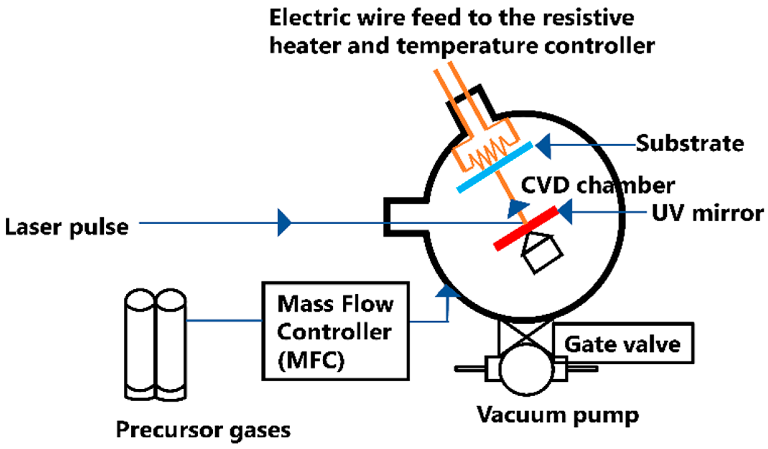
2. Experimental Setup
2.1. Nd:YAG Laser
2.2. Characterization: Raman Spectroscopy
3. Result Analysis
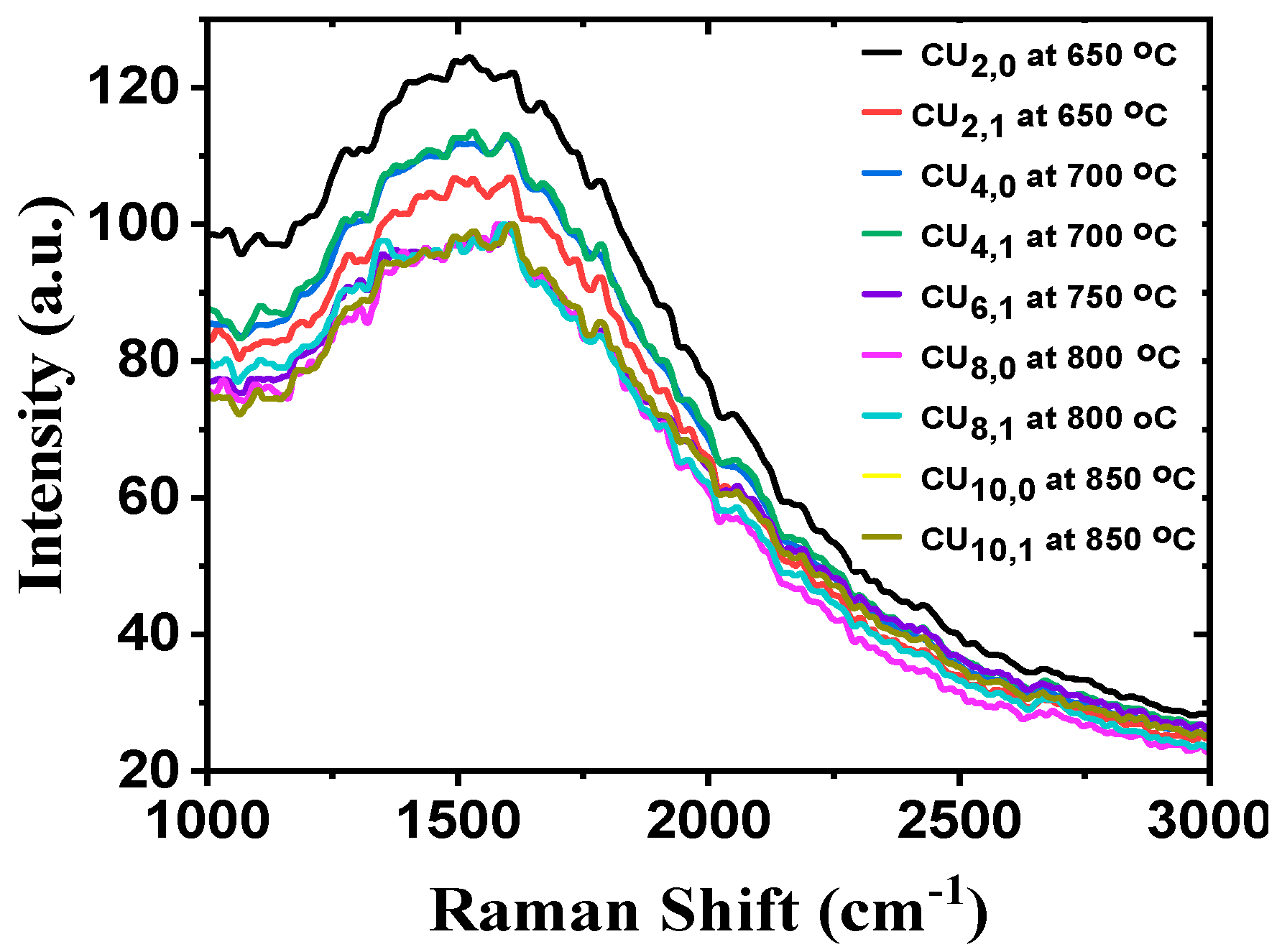
3.1. Variation in CH4 Flow Rate and Temperature
3.1.1. Constant CH4 Flow Rate at 10 sccm and Varied Temperature
3.1.2. Constant CH4 Flow Rate at 20 sccm and at Different Temperatures
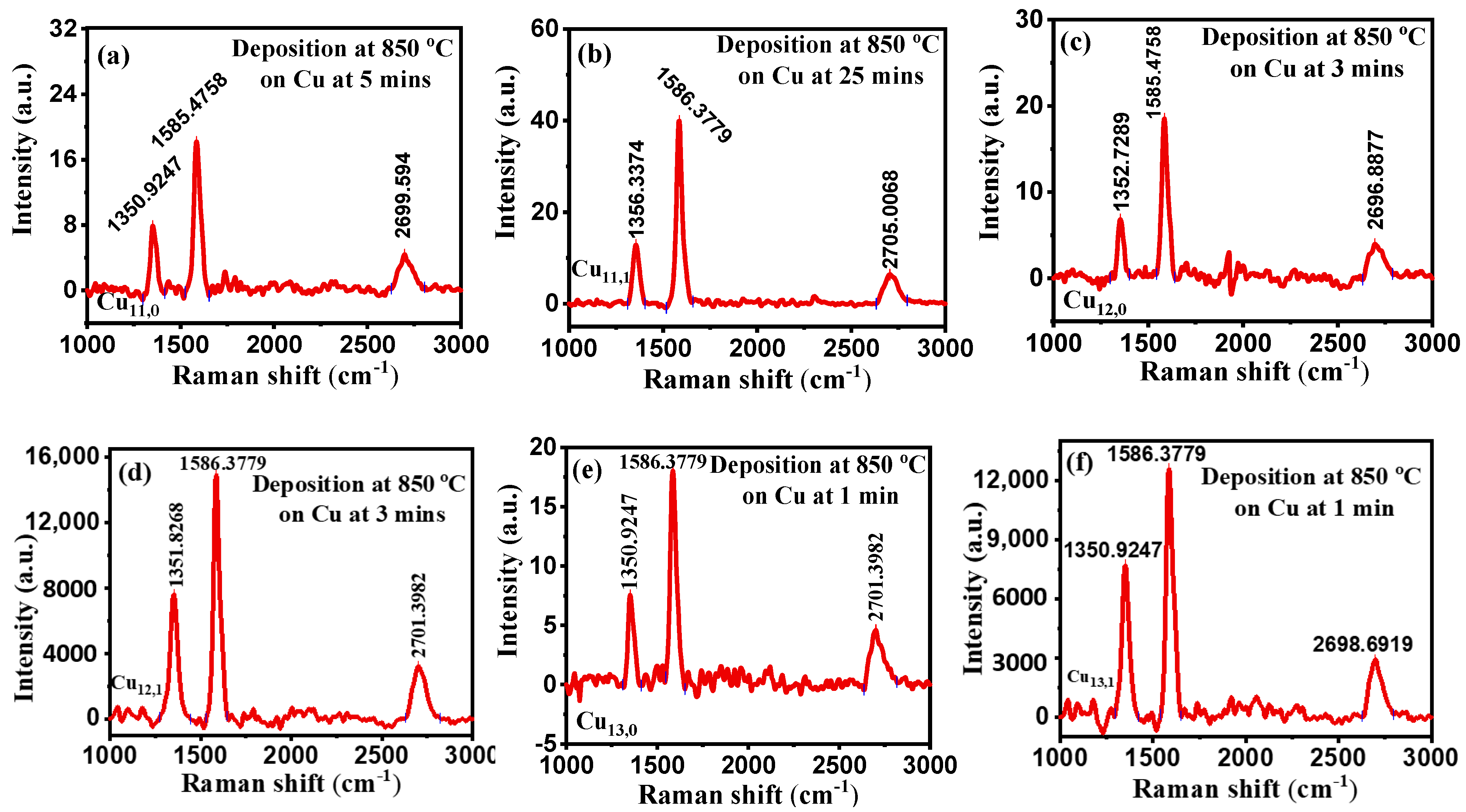
3.2. Variation in Deposition Time
3.3. Effects of Laser Energy on PyC Deposition
3.4. Effects of the Different Substrates on PyC Deposition
3.5. Reaction Mechanism for PyC Deposition
3.6. Quantitative Analysis of Results
4. Conclusions
Author Contributions
Funding
Institutional Review Board Statement
Informed Consent Statement
Data Availability Statement
Acknowledgments
Conflicts of Interest
References
- Sabzehmeidani, M.M.; Mahnaee, S.; Ghaedi, M.; Heidari, H.; Roy, V.A.L. Carbon based materials: A review of adsorbents for inorganic and organic compounds. Mater. Adv. 2021, 2, 598–627. [Google Scholar] [CrossRef]
- Frackowiak, E. Carbon materials for supercapacitor application. Phys. Chem. Chem. Phys. 2007, 9, 1774–1785. [Google Scholar] [CrossRef]
- Pandolfo, A.; Hollenkamp, A.F. Carbon properties and their role in supercapacitors. J. Power Sources 2006, 157, 11–27. [Google Scholar] [CrossRef]
- McCallion, C.; Burthem, J.; Rees-Unwin, K.; Golovanov, A.; Pluen, A. Graphene in therapeutics delivery: Problems, solutions and future opportunities. Eur. J. Pharm. Biopharm. 2016, 104, 235–250. [Google Scholar] [CrossRef]
- Kumar, R.; del Pino, A.P.; Sahoo, S.; Singh, R.K.; Tan, W.K.; Kar, K.K.; Matsuda, A.; Joanni, E. Laser processing of graphene and related materials for energy storage: State of the art and future prospects. Prog. Energy Combust. Sci. 2022, 100981. [Google Scholar] [CrossRef]
- Yazdi, G.R.; Iakimov, T.; Yakimova, R. Epitaxial Graphene on SiC: A Review of Growth and Characterization. Crystals 2016, 6, 53. [Google Scholar] [CrossRef] [Green Version]
- Bourlinos, A.B.; Georgakilas, V.; Zboril, R.; Steriotis, T.A.; Stubos, A.K. Liquid-Phase Exfoliation of Graphite Towards Solubilized Graphenes. Small 2009, 5, 1841–1845. [Google Scholar] [CrossRef]
- Xu, Y.; Cao, H.; Xue, Y.; Li, B.; Cai, W. Liquid-Phase Exfoliation of Graphene: An Overview on Exfoliation Media, Techniques, and Challenges. Nanomaterials 2018, 8, 942. [Google Scholar] [CrossRef] [Green Version]
- Zhang, J.; Yang, H.; Shen, G.; Cheng, P.; Zhang, J.; Guo, S. Reduction of graphene oxide vial-ascorbic acid. Chem. Commun. 2010, 46, 1112–1114. [Google Scholar] [CrossRef]
- Bhuyan, A.; Uddin, N.; Islam, M.; Bipasha, A.; Hossain, S. Synthesis of graphene. Int. Nano Lett. 2016, 6, 65–83. [Google Scholar] [CrossRef] [Green Version]
- Fidanova, T.; Petrov, S.; Napoleonov, B.; Marinova, V.; Petrova, D.; Rafailov, P.; Lin, S.H.; Dimitrov, D. Single and multilayer graphene grown by CVD technique: Characterization for electro-optical applications. In Proceedings of the AIP Conference Proceedings, Sofia, Bulgaria, 26 February 2019; p. 020017. [Google Scholar] [CrossRef]
- Wang, J.; Ren, Z.; Hou, Y.; Yan, X.-L.; Liu, P.-Z.; Zhang, H.; Zhang, H.; Guo, J. A review of graphene synthesis at low temperatures by CVD methods. New Carbon Mater. 2020, 35, 193–208. [Google Scholar] [CrossRef]
- Ren, J.; Zhao, D.; Qi, F.; Liu, W.; Chen, Y. Heat and hydrothermal treatments on the microstructure evolution and mechanical properties of plasma sprayed hydroxyapatite coatings reinforced with graphene nanoplatelets. J. Mech. Behav. Biomed. Mater. 2020, 101, 103418. [Google Scholar] [CrossRef]
- Li, C.; Yang, Z.; Tang, Z.; Guo, B.; Tian, M.; Zhang, L. A scalable strategy for constructing three-dimensional segregated graphene network in polymer via hydrothermal self-assembly. Chem. Eng. J. 2019, 363, 300–308. [Google Scholar] [CrossRef]
- Duty, C.; Jean, D.; Lackey, W. Laser chemical vapour deposition: Materials, modelling, and process control. Int. Mater. Rev. 2001, 46, 271–287. [Google Scholar] [CrossRef]
- Zahid, M.U.; Pervaiz, E.; Hussain, A.; Shahzad, M.I.; Niazi, M.B.K. Synthesis of carbon nanomaterials from different pyrolysis techniques: A review. Mater. Res. Express 2018, 5, 052002. [Google Scholar] [CrossRef]
- Collins, P.; Avouris, P. Nanotubes for electronics. Sci. Am. 2000, 283, 62–69. [Google Scholar] [CrossRef]
- Ross, M.; James, C.; Couzens, G.; Klawitter, J. Pyrocarbon small joint arthroplasty of the extremities. In Joint Replacement Technology; Elsevier: Amsterdam, The Netherlands, 2014; pp. 628–673. [Google Scholar]
- López-Honorato, E.; Meadows, P.J.; Xiao, P. Fluidized bed chemical vapor deposition of pyrolytic carbon–I. Effect of deposition conditions on microstructure. Carbon 2009, 47, 396–410. [Google Scholar] [CrossRef]
- McEvoy, N.; Peltekis, N.; Kumar, S.; Rezvani, E.; Nolan, H.; Keeley, G.P.; Blau, W.; Duesberg, G.S. Synthesis and analysis of thin conducting pyrolytic carbon films. Carbon 2012, 50, 1216–1226. [Google Scholar] [CrossRef]
- Hu, Z.J.; Zhang, W.G.; Hüttinger, K.J.; Reznik, B.; Gerthsen, D. Influence of pressure, temperature and surface area/volume ratio on the texture of pyrolytic carbon deposited from methane. Carbon 2003, 41, 749–758. [Google Scholar] [CrossRef]
- Chen, M.; Zhu, Y.; Xia, J.; Wu, H. Molecular insights into the initial formation of pyrolytic carbon upon carbon fiber sur-face. Carbon 2019, 148, 307–316. [Google Scholar] [CrossRef]
- Saeed, M.; Alshammari, Y.; Majeed, S.A.; Al-Nasrallah, E. Chemical vapour deposition of graphene—Synthesis, charac-terisation, and applications: A review. Molecules 2020, 25, 3856. [Google Scholar] [CrossRef]
- Shah, A.; Stenberg, P.; Karvonen, L.; Ali, R.; Honkanen, S.; Lipsanen, H.; Peyghambarian, N.; Kuittinen, M.; Svirko, Y.; Kaplas, T. Pyrolytic carbon coated black silicon. Sci. Rep. 2016, 6, 25922. [Google Scholar] [CrossRef] [Green Version]
- Lobo, L.S.; Carabineiro, S.A.C. Carbon Formation at High Temperatures (550–1400 °C): Kinetics, Alternative Mechanisms and Growth Modes. Catalysts 2020, 10, 465. [Google Scholar] [CrossRef]
- Wu, Y.; Wang, S.; Komvopoulos, K. A review of graphene synthesis by indirect and direct deposition methods. J. Mater. Res. 2020, 35, 76–89. [Google Scholar] [CrossRef]
- Kumar, R.; Singh, R.K.; Singh, D.; Joanni, E.; Yadav, R.M.; Moshkalev, S.A. Laser-assisted synthesis, reduction and micro-patterning of graphene: Recent progress and applications. Coord. Chem. Rev. 2017, 342, 34–79. [Google Scholar] [CrossRef]
- Barberio, M.; Antici, P. Laser-Plasma Driven Synthesis of Carbon-Based Nanomaterials. Sci. Rep. 2017, 7, 12009. [Google Scholar] [CrossRef] [Green Version]
- Kim, B.J.; Nasir, T.; Choi, J.-Y. Direct Growth of Graphene at Low Temperature for Future Device Applications. J. Korean Ceram. Soc. 2018, 55, 203–223. [Google Scholar] [CrossRef] [Green Version]
- Diode Laser Pumped Nd: YAG Laser. Available online: https://www.tau.ac.il/~lab3/72_laser_res/yag_manual.pdf (accessed on 20 March 2021).
- Hu, S.; Lee, C.-Y.; Chiu, H.-T. Chemical Vapor Deposition of Carbon Nanocoils Three-Dimensionally in Carbon Fiber Cloth for All-Carbon Supercapacitors. ACS Omega 2019, 4, 195–202. [Google Scholar] [CrossRef] [Green Version]
- Dovbeshko, G.I.; Romanyuk, V.R.; Pidgirnyi, D.V.; Cherepanov, V.V.; Andreev, E.O.; Levin, V.M.; Kuzhir, P.P.; Kaplas, T.; Svirko, Y.P. Optical Properties of Pyrolytic Carbon Films Versus Graphite and Graphene. Nanoscale Res. Lett. 2016, 10, 234. [Google Scholar] [CrossRef] [Green Version]
- Gajewski, G.; Pao, C.-W. Ab initio calculations of the reaction pathways for methane decomposition over the Cu (111) surface. J. Chem. Phys. 2011, 135, 064707. [Google Scholar] [CrossRef]
- Faggio, G.; Grillo, R.; Foti, A.; Agnello, S.; Messina, F.; Messina, G. Micro-photoluminescence of Carbon Dots Deposited on Twisted Double-Layer Graphene Grown by Chemical Vapor Deposition. ACS Appl. Mater. Interfaces 2021, 13, 7324–7333. [Google Scholar] [CrossRef]


| Sample ID | Process Parameters | |||
|---|---|---|---|---|
| Temp (°C) | Laser Pulse Frequency (Hz) | CH4 Flow Rate (sccm) | Deposition Time (min) | |
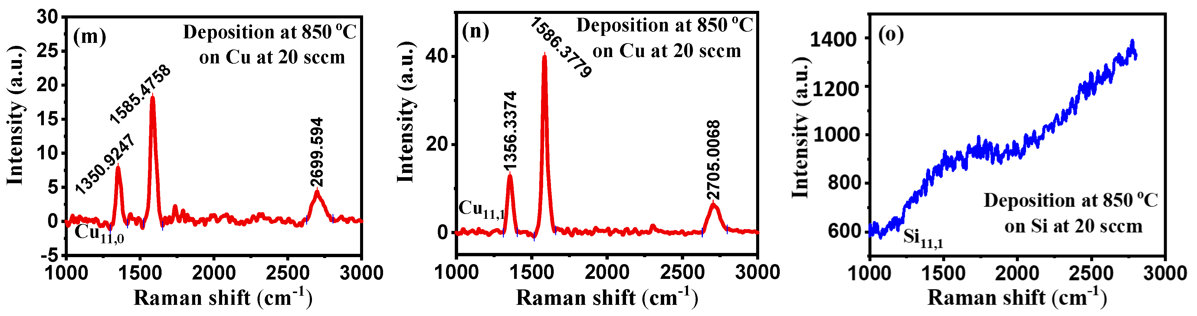
| Cu11,0 | 850 | 10 | 20 | 5 |
| Cu11,1 | 850 | 10 | 20 | 5 |
| Cu12,0 | 850 | 10 | 20 | 3 |
| Cu12,1 | 850 | 10 | 20 | 3 |
| Cu13,0 | 850 | 10 | 20 | 1 |
| Cu13,1 | 850 | 10 | 20 | 1 |
| Sample ID | Process Parameters | ||||
|---|---|---|---|---|---|
| Temp (°C) | Laser Pulse Frequency (Hz) | CH4 Flow Rate (sccm) | Deposition Time (min) | ||
| Cu11,0 | 850 | 10 | 20 | 5 | |
| Si11,1 | Cu11,1 | 850 | 10 | 20 | 5 |
| Cu14,0 | 850 | 0 | 20 | 5 | |
| Number of Graphene Layers | Approximate Peak Intensities | |
|---|---|---|
| Single layer | ||
| Double layer | ||
| Few layers | ||
| Multi-layer | ||
| ID | Peak Position | Peak Intensity | Peak Area | ||||||||
|---|---|---|---|---|---|---|---|---|---|---|---|
| D | G | 2D | D | G | 2D | D | G | 2D | |||
| Cu7,1 | 1351 | 1585 | 2702 | 5.5 | 14.3 | 4.2 | 0.3 | 267.1 | 548.4 | 377.4 | 0.7 |
| Cu9,0 | 1352 | 1586 | 2697 | 237.3 | 612.9 | 142.3 | 0.2 | 8828.0 | 27,855.0 | 11,766.2 | 0.4 |
| Cu9,1 | 1351 | 1586 | 2699 | 234.2 | 621.5 | 155.2 | 0.3 | 9723.4 | 24,434.8 | 13,616.0 | 0.6 |
| Cu11,0 | 1350 | 1585 | 2699 | 7.8 | 18.3 | 4.2 | 0.2 | 294.9 | 822.5 | 330.7 | 0.4 |
| Cu11,1 | 1354 | 1586 | 2704 | 9.1 | 26.0 | 5.1 | 0.2 | 451.4 | 1157.6 | 401.9 | 0.4 |
| Cu12,0 | 1351 | 1585 | 2697 | 6.9 | 18.3 | 3.8 | 0.2 | 263.6 | 752.8 | 350.1 | 0.5 |
| Cu12,1 | 1352 | 1586 | 2701 | 6858 | 14,769 | 3103 | 0.2 | 320,096.0 | 644,120.2 | 249,714.2 | 0.4 |
| Cu13,0 | 1350 | 1586 | 2701 | 8.6 | 18.1 | 4.5 | 0.3 | 427.3 | 792.3 | 365.5 | 0.5 |
| Cu13,1 | 1350 | 1586 | 2698 | 7607 | 12,899 | 3008 | 0.2 | 366,476 | 633,137 | 250,835 | 0.4 |
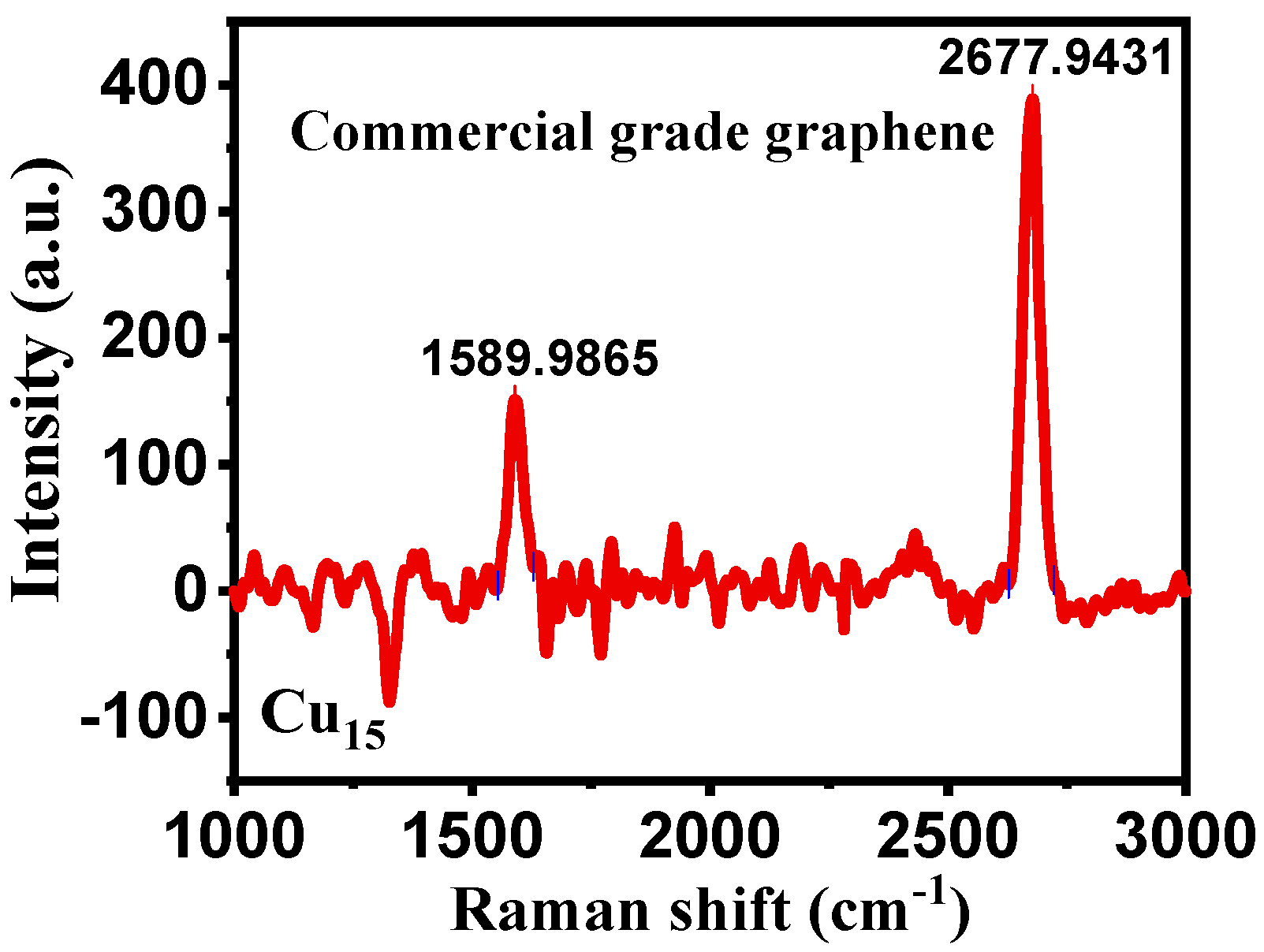
| Cu15 | 0 | 1589 | 2677 | 0 | 140.6 | 375.4 | 2.7 | 0 | 5129.9 | 15,718.5 | 3.1 |
Publisher’s Note: MDPI stays neutral with regard to jurisdictional claims in published maps and institutional affiliations. |
© 2022 by the authors. Licensee MDPI, Basel, Switzerland. This article is an open access article distributed under the terms and conditions of the Creative Commons Attribution (CC BY) license (https://creativecommons.org/licenses/by/4.0/).
Share and Cite
Odusanya, A.; Rahaman, I.; Sarkar, P.K.; Zkria, A.; Ghosh, K.; Haque, A. Laser-Assisted Growth of Carbon-Based Materials by Chemical Vapor Deposition. C 2022, 8, 24. https://doi.org/10.3390/c8020024
Odusanya A, Rahaman I, Sarkar PK, Zkria A, Ghosh K, Haque A. Laser-Assisted Growth of Carbon-Based Materials by Chemical Vapor Deposition. C. 2022; 8(2):24. https://doi.org/10.3390/c8020024
Chicago/Turabian StyleOdusanya, Abiodun, Imteaz Rahaman, Pallab Kumar Sarkar, Abdelrahman Zkria, Kartik Ghosh, and Ariful Haque. 2022. "Laser-Assisted Growth of Carbon-Based Materials by Chemical Vapor Deposition" C 8, no. 2: 24. https://doi.org/10.3390/c8020024
APA StyleOdusanya, A., Rahaman, I., Sarkar, P. K., Zkria, A., Ghosh, K., & Haque, A. (2022). Laser-Assisted Growth of Carbon-Based Materials by Chemical Vapor Deposition. C, 8(2), 24. https://doi.org/10.3390/c8020024