Article

Improving the Performance of Printable Carbon Electrodes by Femtosecond Laser Treatment

by
Marco Girolami
1,*,
Alessandro Bellucci
1,
Matteo Mastellone
1,2,
Valerio Serpente
1,
Stefano Orlando
3,
Veronica Valentini
1,
Alessandro L. Palma
4,5,
Aldo Di Carlo
1,5,6 and
Daniele M. Trucchi
1
1
Istituto di Struttura della Materia, Consiglio Nazionale delle Ricerche (ISM-CNR), Sede Secondaria di Montelibretti, DiaTHEMA Lab, Via Salaria km 29.300, Monterotondo Stazione, 00015 Roma, Italy
2
Dipartimento di Scienze di Base ed Applicate per l’Ingegneria, Università di Roma “La Sapienza”, Piazzale Aldo Moro 5, 00185 Roma, Italy
3
Istituto di Struttura della Materia, Consiglio Nazionale delle Ricerche (ISM-CNR), Sede Secondaria di Tito Scalo, Area Industriale—Contrada S. Loia, Tito Scalo, 85050 Potenza, Italy
4
ENEA, Centro Ricerche Casaccia, Via Anguillarese 301, S. Maria di Galeria, 00123 Roma, Italy
5
C.H.O.S.E. (Centre for Hybrid and Organic Solar Energy), Department of Electronic Engineering, University of Rome Tor Vergata, Via del Politecnico 1, 00133 Roma, Italy
6
LASE-Laboratory for Advanced Solar Energy, National University of Science and Technology “MISiS”, Leninskiy prospect 6, 119049 Moscow, Russia
*
Author to whom correspondence should be addressed.
Submission received: 24 June 2020 / Revised: 10 July 2020 / Accepted: 14 July 2020 / Published: 16 July 2020

Abstract

:
Low-cost carbon-conductive films were screen-printed on a Plexiglas® substrate, and then, after a standard annealing procedure, subjected to femtosecond (fs) laser treatments at different values of total accumulated laser fluence ΦA. Four-point probe measurements showed that, if ΦA > 0.3 kJ/cm2, the sheet resistance of laser-treated films can be reduced down to about 15 Ω/sq, which is a value more than 20% lower than that measured on as-annealed untreated films. Furthermore, as pointed out by a comprehensive Raman spectroscopy analysis, it was found that sheet resistance decreases linearly with ΦA, due to a progressively higher degree of crystallinity and stacking order of the graphitic phase. Results therefore highlight that fs-laser treatment can be profitably used as an additional process for improving the performance of printable carbon electrodes, which have been recently proposed as a valid alternative to metal electrodes for stable and up-scalable perovskite solar cells.

1. Introduction

Perovskite solar cells (PSCs) [1] have been massively investigated in the past few years because of their unique features, e.g., cost-effectiveness and high conversion efficiency (>20% for single-junction PSCs [2], and ~30% for “hybrid” perovskite/silicon tandem solar cells [3]), which make them very competitive with the conventional silicon-based devices. Two main factors have hampered PSCs from entering the commercial market up to now, namely: (1) a limited operational stability with time and temperature [4], and (2) up-scalability issues. On the one hand, new technologies have been recently developed which have been demonstrated to improve PSCs stability [5,6], however, on the other hand, industrial production is still far from starting, mostly due to the lack of cost-effective fabrication methods on a large scale. For instance, at a lab scale, high conversion efficiency is achieved using counter-electrodes made with noble metals, mainly silver (Ag) and gold (Au). Both of them show excellent conductivity and a suitable work function, which are mandatory prerequisites to efficiently extract, collect and transfer charge carriers. However, Ag and Au electrodes are usually fabricated by means of time-consuming standard lithographic processes, requiring expensive clean-room facilities which do not fit with industrial mass manufacturing. Moreover, it is worth mentioning here that noble metal electrodes may also affect long-term stability of PSCs: both Au and Ag can indeed react with the halide (iodide) ions in the hybrid perovskite, due to a combined effect of perovskite decomposition and metal migration, thus contributing significantly to the device degradation process [7,8].
In such a context, carbon electrodes have recently been demonstrated to be promising candidates for replacing noble metal counter-electrodes in PSCs [9]. Carbon is chemically stable; moreover, conductive carbon films show a work function (~5.0 eV) similar to that of polycrystalline Au films (~5.1 eV) [9]. But most of all, in the form of paste (obtained from carbon black, graphite powder and a proper binder), carbon is available as a low-cost material for electrode fabrication by screen-printing [10], which is a simple, reliable, cost-effective and reproducible method suitable for industrial mass production. Nevertheless, the sheet resistance of carbon electrodes obtained from commercial carbon paste (10–100 Ω/sq) is still considerably higher than that of noble metal electrodes (<1 Ω/sq), thus creating a bottleneck for charge carriers due to the introduction of a significant series resistance [11].
Generally speaking, the improvement of electrical conductivity of carbon-based materials is a hot topic in a wide range of research fields, and several methodologies can be applied to reach the goal. Some of them are based on mechanical processes. For instance, a significant decrease of the sheet resistance of carbon nanostructured thin films, composed of graphene nanosheets and multiwalled carbon nanotubes (CNTs), can be obtained by a combination of compression and polishing [12]. Recently, a simple grinding process in a household coffee grinder was demonstrated to increase the electrical conductivity of carbon nanotubes [13]. Chemical treatments can also be performed. Immersion in nitric acid, followed by exposure to fuming nitric acid, was demonstrated to be effective in inducing p-type doping in graphene-CNT films [14], whereas fluorination of carbon black can be efficiently used to improve the electrical conductivity of electrospun carbon fibers [15]. The most common methodology to reduce electrical resistivity is undoubtedly thermal annealing, which can be successfully applied to a wide range of carbon-based materials, spanning from CNT aerogels [16] to biochar [17], from graphene [18] to glassy carbon [19]. As regards screen-printed carbon electrodes, thermal annealing at temperatures up to 400 °C is a recommended practice to decrease the sheet resistance, mostly for two reasons: (1) it promotes inter-particle contact, implying an easier charge transfer across the film, and (2) it increases the graphitization degree of the carbon film, at the same time reducing the concentration of defects in the graphitized regions [20]. Indeed, it is well known that the electrical conductivity of a carbon film increases with the extent of sp2-bonded carbon in its microstructure, as well as with the degree of structural order of such graphitic sp2 domains.
Now, the main effect of the irradiation of a carbon film with femtosecond (fs) laser pulses (having a fluence below the ablation threshold) is to increase the sp2 to sp3 hybridization ratio, therefore favoring graphitization. More interestingly, this happens independently from the degree of crystallinity of the film under treatment. Graphitization induced by ultrashort (<1 ps) laser pulses has indeed been observed in amorphous carbon [21], diamond-like carbon [22], as well as in chemical vapor deposition single-crystal [23,24] and polycrystalline [25] diamond films. Taking a cue from these results, we investigated on the possibility of further decreasing the sheet resistance of annealed screen-printed carbon electrodes by fs-laser treatment. Our results show that, by a proper choice of the total accumulated laser fluence delivered to the carbon film, it is possible to decrease the sheet resistance by more than 20% with respect to the as-annealed untreated film, thus demonstrating that fs-laser processing can significantly improve the performance of printable carbon electrodes for PSCs.

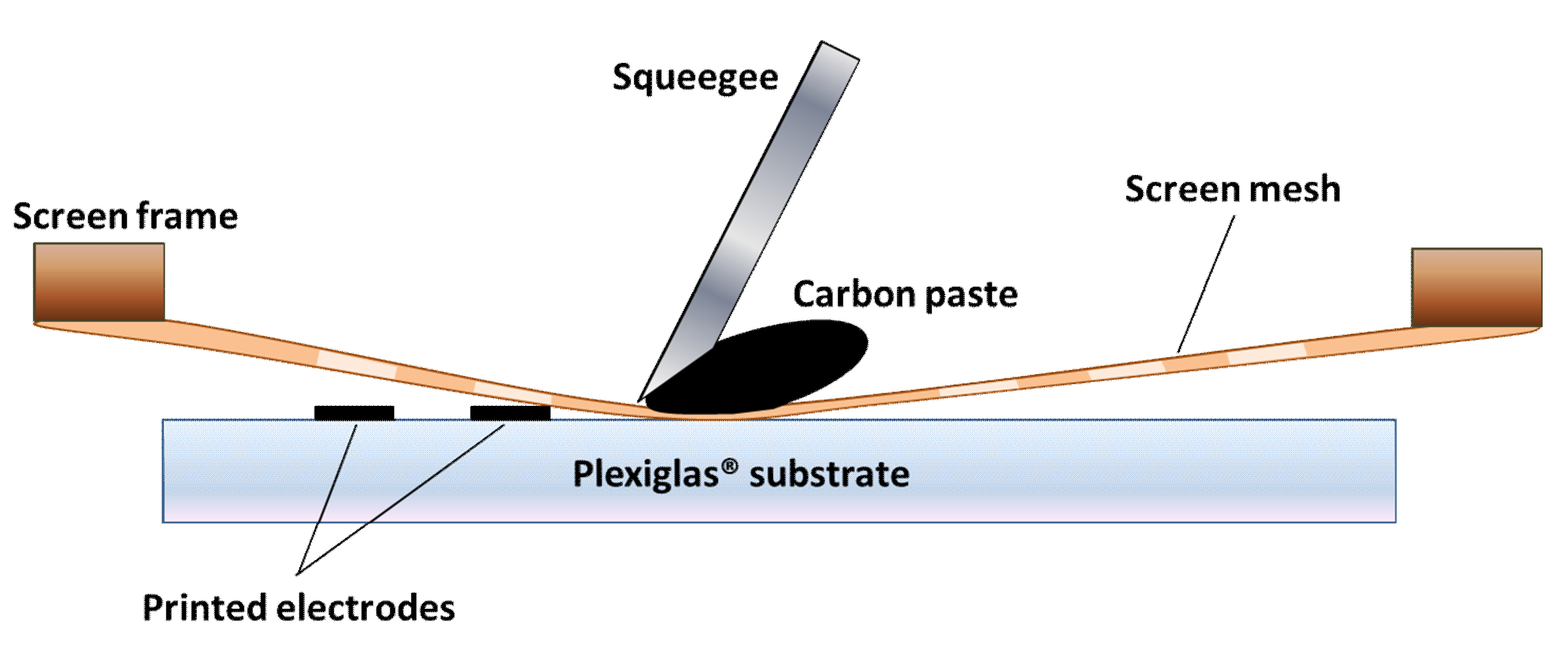
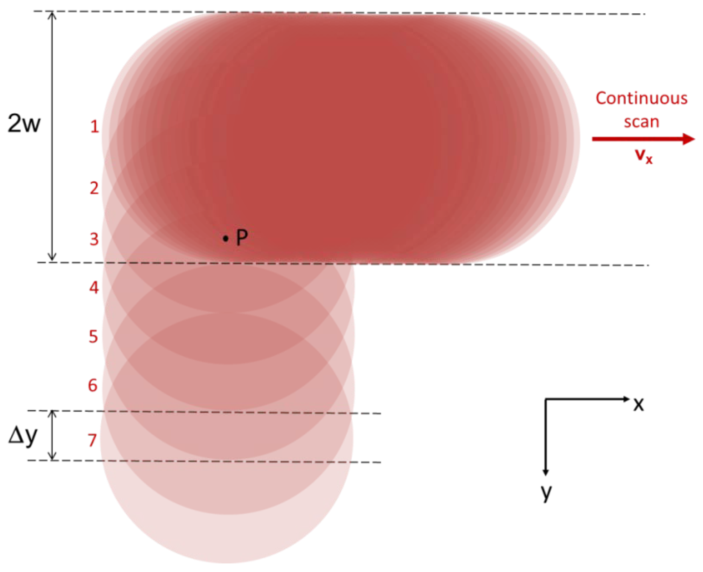
2. Materials and Methods

A colorless 3 mm-thick Plexiglas® plate, with nominal electrical resistivity > 1011 Ω cm, was used as a substrate for the deposition of printable carbon electrodes. Before deposition, the substrate was cleaned in an ultrasonic bath with acetone for 5 min, then with isopropanol for a further 5 min. Successively, the substrate was rinsed with deionized water and dried in pure nitrogen flow.
An array of carbon strips, with lateral dimensions 2 × 10 cm2, was deposited on the substrate with a screen-printing technique (see Figure 1). A nylon flexible screen mesh, on which the pattern to be printed was previously defined, was held over the substrate by a rigid screen frame. Then, an adequate amount of commercial carbon paste (Elcocarb B/SP from Solaronix, Aubonne, Switzerland) was applied on the screen mesh. A polyurethane flexible squeegee (Shore hardness grade 70) was moved all along the screen mesh, pressing it down into contact with the substrate; in this way, carbon paste was progressively pushed through the screen mesh and deposited onto the surface of the Plexiglas® plate. The as-deposited carbon strips were finally annealed on a hot plate at 400 °C for 30 min, as recommended by the producer to minimize sheet resistivity. It is worth mentioning here that, unlike what was reported in Reference [20], the heating procedure at temperatures > 300 °C did not cause deformation of the annealed carbon strips.
The laser treatments were performed (at room temperature and in air) by using a linearly polarized femtosecond pulsed laser beam, produced by a regeneratively amplified mode-locked “chirped-pulse” Ti: sapphire laser (wavelength λfs = 800 nm). Pulse duration, τ, was ~100 fs. Repetition rate, f, was 1 kHz. The Plexiglas® plate hosting the printed carbon strips was positioned on an automatically controlled micrometric x-y translational stage (Laser μFAB microfabrication Workstation, from Newport, Irvine, CA, USA). For every single treatment, the focused laser beam, with a diameter (1/e2 width) equal to 2w = 500 µm, scanned a limited portion of the surface of the carbon strips (namely, a 1 × 1 cm2 square) following a raster pattern. As can be easily visualized in Figure 2, the laser beam sweeps horizontally left-to-right at a uniform scanning speed vx, then blanks and rapidly moves back to the left; after that, it shifts vertically by a distance Δy = 100 µm, turns on again, and starts a new horizontal scan, and so on until a 1 × 1 cm2 square is processed.
Aimed at an accurate comparative analysis, six different laser treatments were performed, by varying the total accumulated laser fluence delivered to the surface unit each time (exemplified by the point P in Figure 2). For a single horizontal scan along the x-axis, the accumulated laser fluence is defined as Φx = NxΦp, where Nx is the average number of pulses impinging the surface unit and Φp = Ep/(πw2) is the single pulse laser fluence, with Ep and w being the pulse energy and the circular beam radius on the focal plane, respectively. To obtain the total accumulated laser fluence, ΦA, delivered to the surface unit, however, we have to also take into account the spatial vertical overlap, Δy, between two consecutive horizontal scans (see Figure 2), namely ΦA = (2w/Δy) Φx. In our case, being Δy = 100 μm and 2w = 500 μm, we simply obtain ΦA = 5Φx.
Pulse energy was kept constant for all the different treatments. In particular, the selected pulse energy was Ep = 475 μJ, corresponding to a single pulse laser fluence Φp = 0.24 J/cm2. This choice was made by considering that 0.24 J/cm2 is an intermediate value between the graphitization threshold of amorphous carbon (evaluated to be about 0.2 J/cm2 with a single pulse irradiation at λfs = 800 nm and τ = 100 fs) and the ablation threshold (about 0.3 J/cm2), over which evaporation starts and a smooth “bell-like” crater in the spot center appears [22]. A constant single pulse laser fluence also allowed us to vary the accumulated laser fluence, Φx, by simply acting on the laser scanning speed, vx, which, together with the laser repetition rate, f, defines the average number of pulses, Nx, impinging the surface unit, according to the relationship Nx = 2wf/vx.
Table 1 resumes all the experimental parameters considered for the laser treatment of six different areas (squares #1 to #6) of the screen-printed carbon strips.

3. Results and Discussion

In the following subsections, a comparative analysis of the different fs-laser-treated screen-printed carbon films will be introduced and phenomenologically discussed, aimed at finding a possible relationship between the electrical properties and the structural modifications induced by the laser treatments.

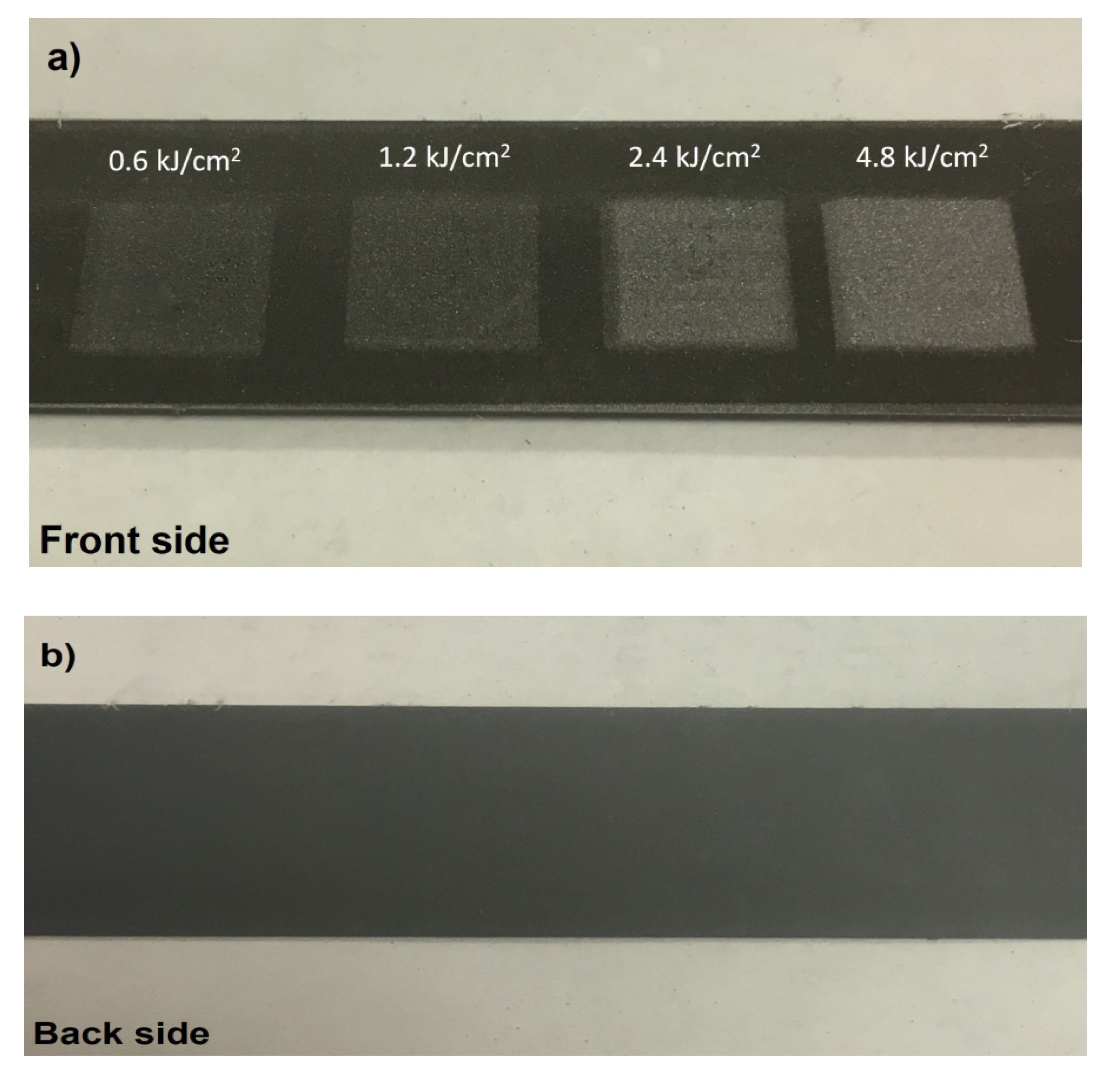
3.1. Visual Inspection

On the basis of a visual inspection performed soon after the treatment, no noticeable differences were observed between the untreated areas of the carbon strips and the squares treated at the two lowest values of total accumulated laser fluence (i.e., ΦA = 0.15 kJ/cm2 and ΦA = 0.3 kJ/cm2). Conversely, at higher ΦA values, the color of treated areas turns from deep black to gray, and the square shapes emerge from the background (Figure 3a), clearly pointing out a modification of the material. Moreover, gray color is progressively lighter with increasing ΦA values: by considering that the carbon paste used in this work is composed of micrometric graphite particles and carbon black nanoparticles (dispersed in a mixture of terpineol, organic binders and inorganic binders) this could suggest an increase of graphite-to-carbon black ratio with increasing total accumulated laser fluence.
It is worth noting here that a lighter color caused by possible thinning of the carbon film, induced by laser ablation, can be excluded in our case: indeed, as can be seen from Figure 3b, showing a back-side view of the treated carbon strip through the transparent Plexiglas® plate, laser-processed squares on the front side surface cannot be seen. Also, the homogeneous deep black color of the back surface of the carbon strip indicates that the laser treatment does not involve the whole thickness of the strip, but, as expected, is limited to the upper layers of the front side.

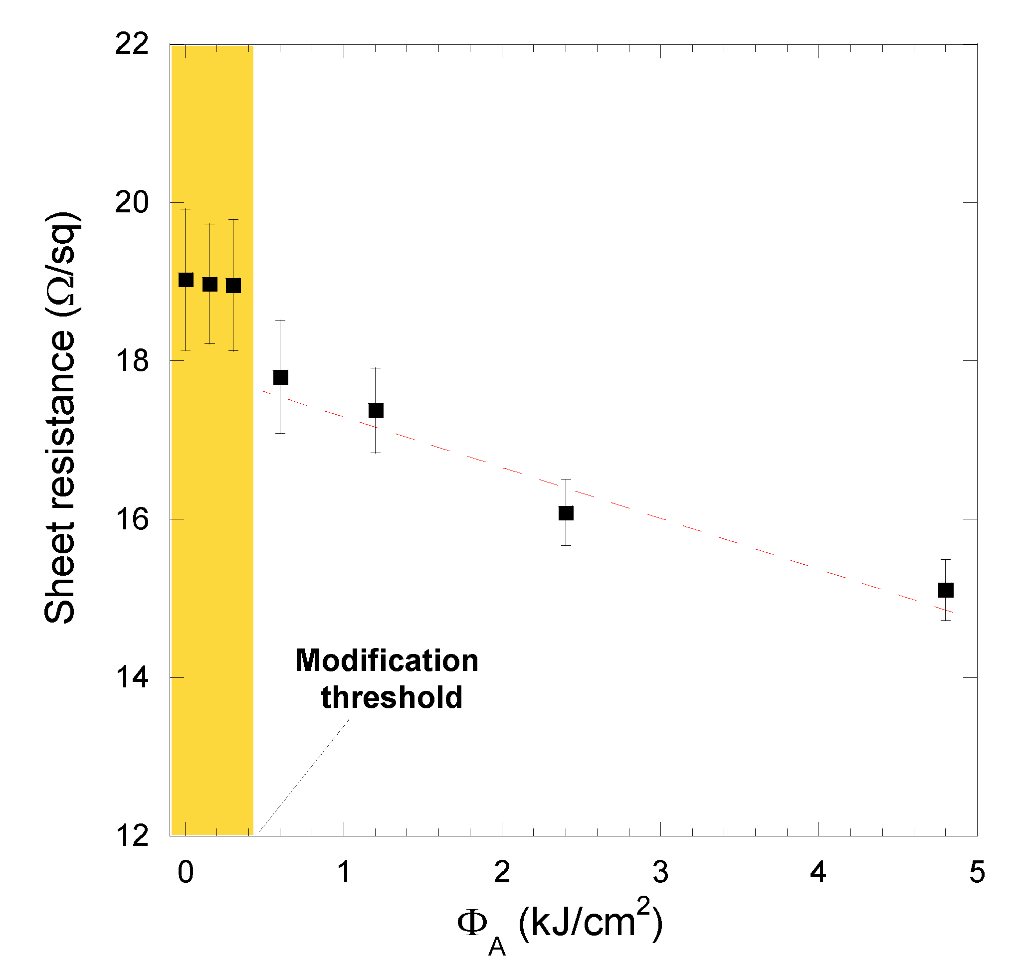
3.2. Four-Point Probe Resistivity Measurements

Electrical sheet resistance of the laser-processed carbon strips was measured with the well-known four-point (4P) probe method. In particular, a collinear 4P probe array was used with a 1 mm inter-probe distance. Therefore, both the film thickness (~15 μm, as measured with a mechanical profilometer after the annealing procedure) and the inter-probe distance were much smaller than the lateral dimensions (1 × 1 cm2) of the samples to be measured. In this case, sheet resistance Rs can be easily calculated as:
R s = π ln 2 ( V I )
where I is the current injected in the sample by the outer pair of probes, and V is the voltage measured by the inner pair of probes. Current was injected by means of a Keithley 6220 current source (Keithley Instruments, Solon, OH, USA), whereas voltage was measured by using a Keithley 2182 nanovoltmeter.
Figure 4 reports the sheet resistance, calculated according to Equation (1), of both the as-annealed untreated and the laser-treated samples as a function of the total accumulated laser fluence. As expected from the results of visual inspection, no significant differences were observed between the sheet resistance of the as-annealed untreated carbon film (ΦA = 0) and those of the samples treated at ΦA ≤ 0.3 kJ/cm2, all measured to be about Rs = 19 Ω/sq (in perfect agreement with what was declared by the carbon paste producer for films annealed at 400 °C for 30 min). Conversely, for ΦA > 0.3 kJ/cm2, it can be observed from Figure 4 that the sheet resistance decreases linearly with the total accumulated laser fluence, reaching a value of Rs = 15.1 Ω/sq for ΦA = 4.8 kJ/cm2, therefore reducing the sheet resistance value measured for the as-annealed untreated carbon by ~20.5%.

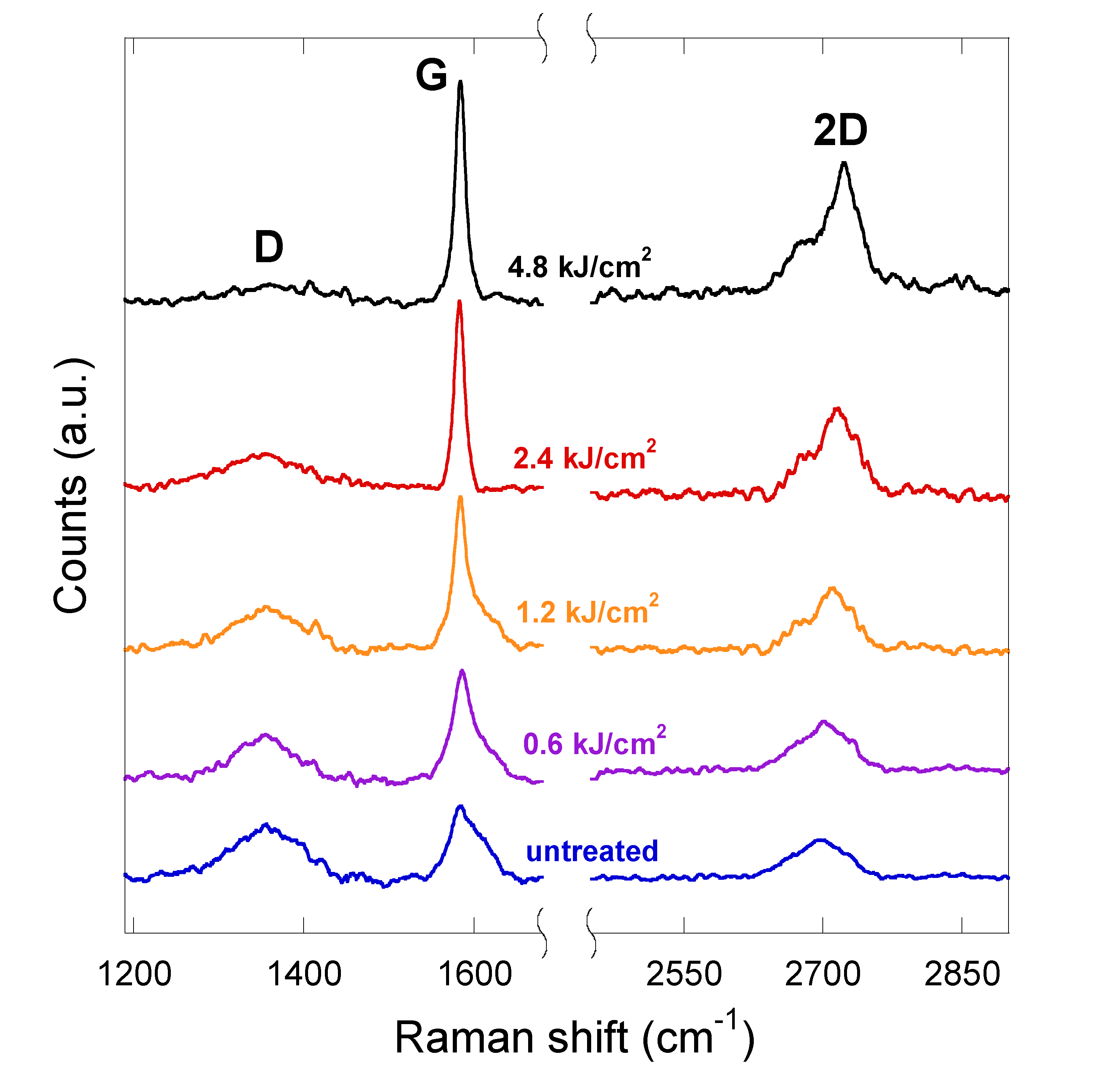
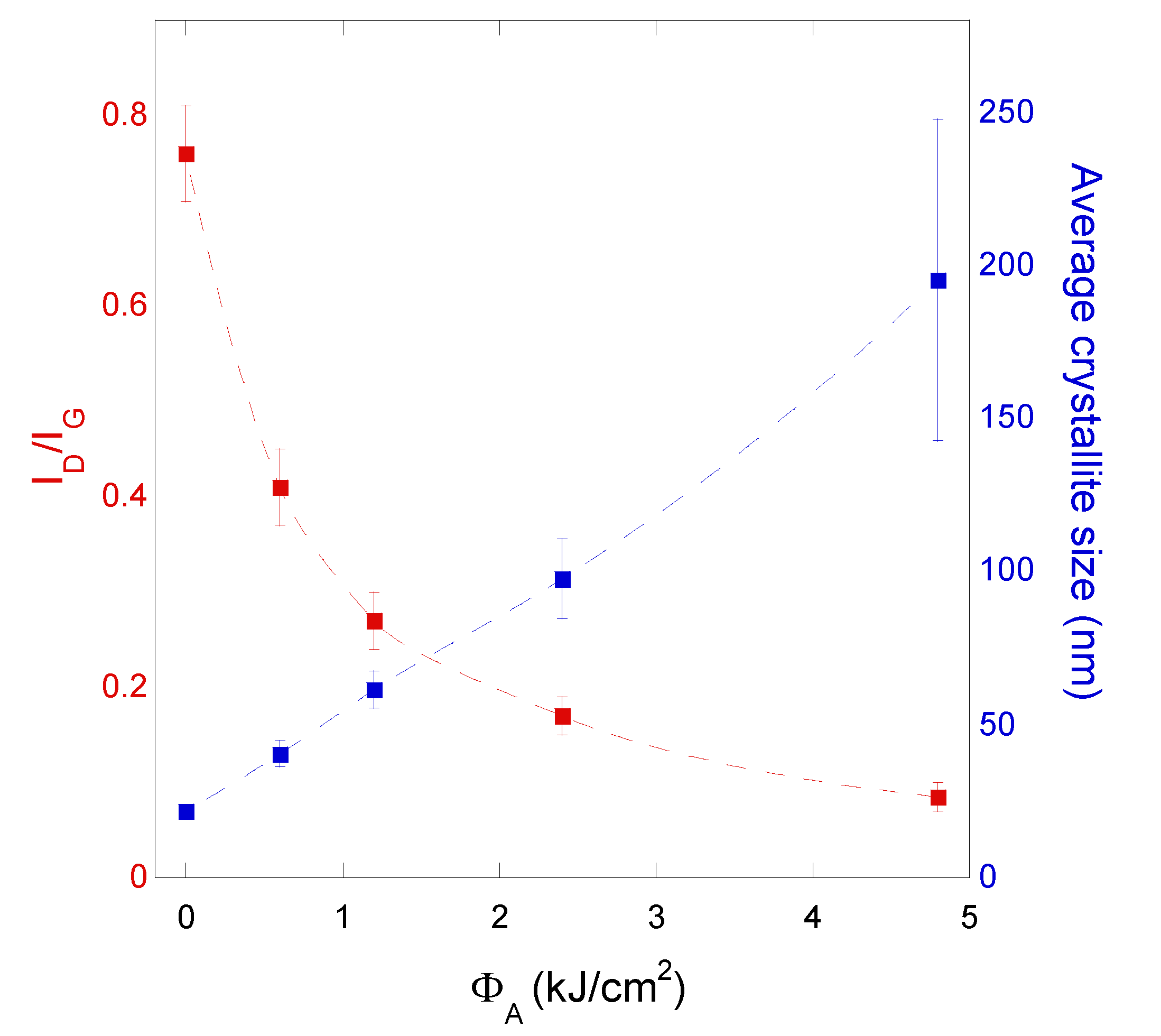
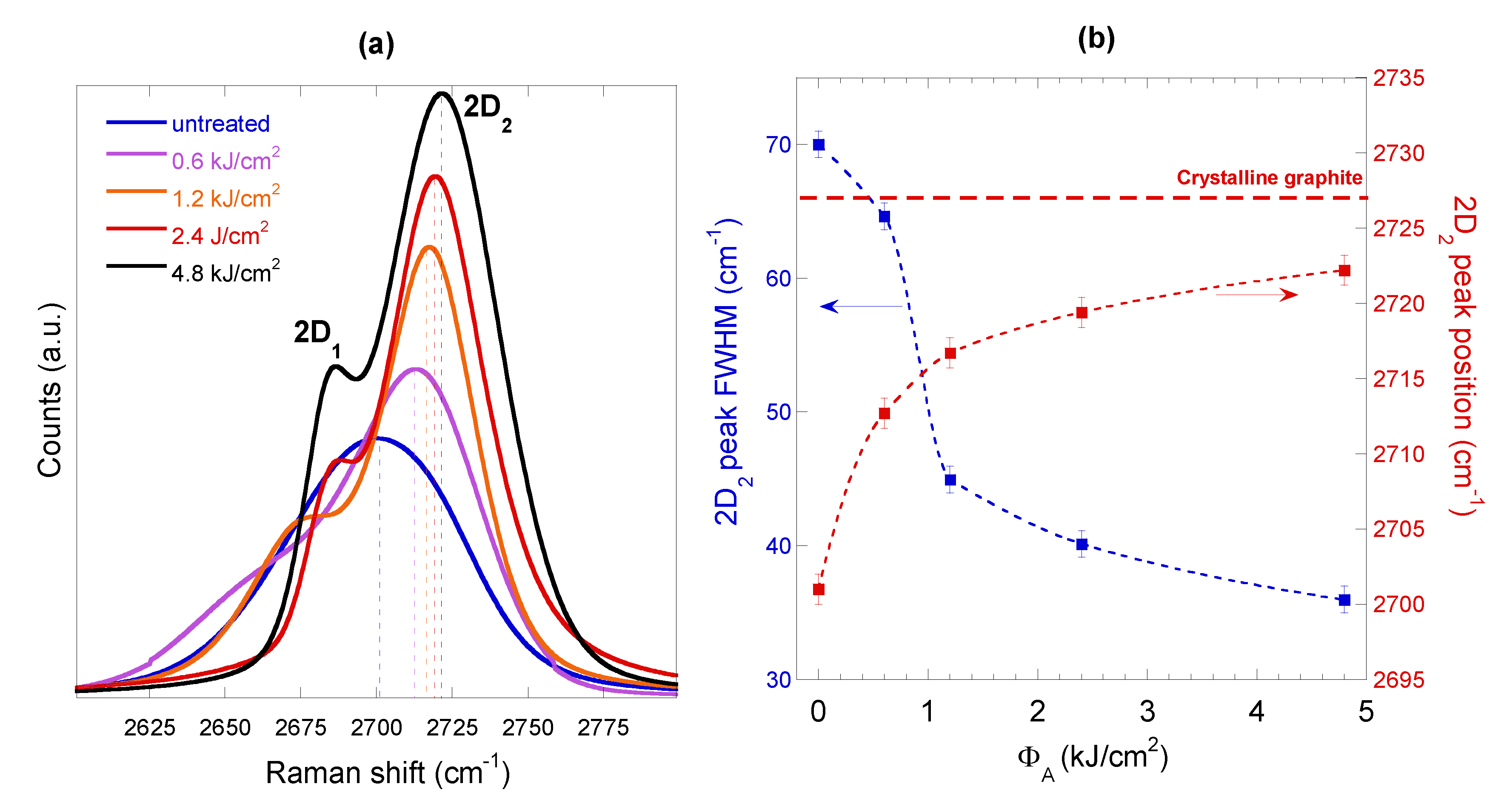
3.3. Raman Characterization

Aimed at understanding if the decrease of the sheet resistance was related to possible structural modifications induced by the fs-laser treatment, an exhaustive Raman characterization was performed on the screen-printed carbon films.
Raman spectra were acquired in the 1050–2950 cm−1 range at room temperature with an Ar+ laser (λR = 514.5 nm wavelength), in back-scattering geometry, using a Dilor XY triple spectrometer (Dilor Instruments SA, Edison, NJ, USA) equipped with a liquid nitrogen-cooled charge coupled device (CCD) detector and an adapted Olympus microscope (Olympus Corporation, Tokyo, Japan) arranged in confocal mode—the spot-size was 2 µm. Spectra were then processed by using the Thermo-Grams Suite v9.2 software (Thermo Fisher Scientific Inc., Waltham, MA, USA) to determine line widths and intensities. Voigt functions were used to fit the peak profiles.
Figure 5 shows the full-range Raman spectra of carbon films treated at different values of total accumulated laser fluence ΦA; for comparison, a typical spectrum recorded from an as-annealed untreated area (ΦA = 0) of the carbon strips is also displayed. As expected for a carbon film, measured spectra show three main features, namely G, D and 2D (G’) bands:
1.
G band is due to the longitudinal optical (LO) and transverse optical (TO) modes of the graphite honeycomb lattice vibration, which degenerate at the center (i.e., the Γ point) of the Brillouin zone, and is characteristic of sp2-hybridized C-C bonds; therefore, it is a fingerprint of graphitic materials.
2.
D and 2D bands are related to double resonance processes. In both cases, an electron–hole pair, generated by the incident laser light, recombines after two electron-phonon scattering events involving phonons with opposite momenta. When a defect is present, one of the scattering events occurs elastically, leading to the D band; conversely, if both the events occur inelastically, the 2D band is generated. That is the reason why D band is the most significant Raman feature related to the amount of disorder in a carbon-based material, whereas 2D band (sometimes indicated in the literature as G’ band) is Raman-active also in a defect-free material.
As a general comment on all the spectra, the contribution of graphite micro-particles to Raman signal prevails over the one given by carbon black nanoparticles. In carbon black, G and D bands overlap [26,27], and the 2D band spreads over a Raman shift range of about 1000 cm−1 [27]; conversely, in our case, G and D bands are well-separated (Figure 5), and the 2D band is always narrower than 200 cm−1, as is commonly observed in graphite-based systems regardless of their structural quality [28,29].
A massive presence of two-dimensional graphitic species, such as graphene oxide or single-layer graphene, can be excluded. In graphene oxide, the integrated intensity of D peak (ID) is indeed higher than the one related to G peak (IG), which is clearly not verified in our case, and the region corresponding to the 2D band (around 2700 cm−1) is substantially flat [27,30,31]. On the other hand, in single-layer graphene, the integrated intensity of the 2D band (I2D) is more than double that of IG [28], whereas in our case, it is always I2D < IG.
We can therefore conclude that both the as-annealed untreated and the laser-treated carbon films are predominantly composed by disordered bulk graphite. The first and clearest effect of the laser treatment is the increasing degree of in-plane structural order with increasing total accumulated laser fluence. As can be directly inferred from Figure 5, the ID/IG ratio, which is the most widely used figure of merit for characterizing the defect quantity in graphitic materials [29], decreases significantly with ΦA. In particular, ID/IG is inversely proportional to ΦA (Figure 6, red curve), which also implies that the average crystallite size, La, increases linearly with ΦA (Figure 6, blue curve), according to the well-known relationship [23]:
L a ( nm ) = 560 E R 4 ( I D I G ) 1
where ER is the excitation energy (in eV) of the laser radiation used for Raman analysis (2.41 eV for a 514.5 nm wavelength).
The hypothesis of a laser-induced evolution towards a less defected graphite with a higher degree of structural order is confirmed by taking a closer look to the G band and 2D band regions of the measured Raman spectra.
As can be seen from Figure 7a, the D’ band, which is another defect-induced Raman feature appearing usually in the 1600–1620 cm−1 range as a “shoulder” of the G peak [29,32], disappears when the highest total accumulated laser fluence values (ΦA = 2.4 kJ/cm2 and ΦA = 4.8 kJ/cm2) are used, thus denoting a lower concentration of defects. An increasing degree of crystallinity with increasing ΦA is also pointed out by a progressively narrower G peak, the full width at half maximum (FWHM) of which decreases with ΦA, as well as by a slight downshift of the G peak position from 1586.3 cm−1 in the as-annealed untreated case to 1582.5 cm−1 when ΦA = 4.8 kJ/cm2 (see Figure 7b), thus approaching 1581 cm−1, which is the reference G peak position for crystalline graphite [32]. According to the three-stage model proposed by Ferrari and Robertson [33], both these effects, along with the disappearance of the D’ band at 1620 cm−1, are indeed always present in the evolution of the Raman spectrum of a carbon film when moving from nanocrystalline graphite to ordered graphite, namely the final stage of the so-called “ordering trajectory”.
On the other hand, the analysis of the 2D band profile in the Raman spectrum of a graphite sample is a powerful tool to assess its degree of stacking order, since the 2D band is very sensitive to structural changes along the c-axis [34]. As can be seen from Figure 8a, the 2D band in the as-annealed untreated case can be fitted by a single Lorentzian centered at 2702.5 cm−1 and having a FWHM of about 70 cm−1, which is the typical 2D band profile of two-dimensional graphite samples [35]. However, the presence of single-layer graphene, which returns a downshifted (in the range 2680–2690 cm−1 [36,37]) and narrower (20–30 cm−1 FWHM [36,38]) peak, should be excluded in our case, as already pointed out by the relationship I2D/IG < 1. More likely, the single 2D peak in the as-annealed untreated case can be attributed to turbostratic graphite, which indeed shows a single 2D peak upshifted by about 20 cm−1 with respect to single-layer graphene, and with an almost double FWHM [34,36].
Now, turbostratic graphite is by definition a three-dimensional graphite with no stacking order between adjacent layers (i.e., with a total lack of c-axis order), and that is the reason why it can be considered as a two-dimensional graphite to first approximation. By observing Figure 8a, in case of laser treatment, the single 2D peak evolves towards a two-peak (namely, 2D1 and 2D2) profile, as observed in graphitic samples formed by a large number (>5) of graphene layers [37], as well as in three-dimensional highly-ordered graphite [32]. Therefore, it can be inferred that fs-laser treatment is able to improve the stacking order of the graphitic phase of screen-printed carbon films. In particular, the degree of stacking order increases with the total accumulated laser fluence, as pointed out by: (1) a progressively narrower 2D2 peak (see Figure 8b), the FWHM of which decreases with ΦA, and (2) a slight upshift of the 2D2 peak position from 2702.5 cm−1 in the as-annealed untreated case to 2722 cm−1 when ΦA = 4.8 kJ/cm2, thus approaching 2727 cm−1, which is the reference 2D2 peak position for crystalline graphite [35].
It is worth noting here that the 2D band Raman spectra reported in Figure 8a are very similar to those measured by Cancado et al. [39] on disordered graphite samples heat-treated at very high temperatures, varying in the range 2200–2700 °C. In that case, the degree of stacking order was observed to increase with the heat-treatment temperature (HTT), as inferred by a 2D (G’) band progressively shifting from a one-peak profile (for HTT = 2200 °C), attributed to turbostratic graphite, to a two-peak profile (for HTT = 2700 °C), attributed to c-axis ordered (i.e., crystalline) graphite. Therefore, a significant phenomenological analogy clearly emerges between heat treatment and fs-laser treatment in increasing the degree of stacking order of graphite, with the total accumulated laser fluence producing the same effects as HTT on the stacking order-related Raman features of the 2D band.
Now, heat treatment at very high temperatures (>2000 °C) is a stationary annealing process, in which heat diffuses throughout the film thickness. Temperature depth profile is constant, so that thermal energy uniformly “heals” defects (e.g., interstitials, stacking faults) of disordered carbon films, in this way increasing the inter-layer interaction between stacked layers [40]. Conversely, in case of fs-laser treatment, pulse duration is so short that heat diffusion is negligible, so that the temperature depth profile at the very end of the laser pulse is similar to the spatial distribution of the absorbed energy, i.e., sharply decreasing from the surface to the bulk. For this reason, as demonstrated by Kononenko et al. in a study on laser-induced graphitization of diamond-like carbon films [22], the thickness of the graphitized layer increases with the number of laser pulses, mostly because more pulses are needed for the inner layers to reach the temperature threshold for graphitization. This may apply to our case. We can indeed hypothesize that an increased degree of stacking order with increasing total accumulated laser fluence (which implies a higher number of laser pulses on the same spot) is strictly connected to a progressively higher depth at which the temperature threshold for graphite “ordering” along the c-axis is reached. Moreover, following this thread, a higher ΦA also implies a higher temperature at a given depth (surface included), which could explain the better in-plane structural quality, as previously inferred from the observation of the G band region.

4. Conclusions

Carbon films obtained by the screen-printing technique from a commercially available carbon paste were subjected to fs-laser processing after a standard annealing procedure. Results show that, if total accumulated laser fluence is higher than 0.3 kJ/cm2, sheet resistance decreases significantly (up to 20.5% less) as a consequence of a laser-induced improvement of the structural quality of the graphitic phase, as inferred from a comprehensive Raman spectroscopy analysis. Therefore, fs-laser treatment following annealing (which is necessary to ensure a proper sintering process of the carbon paste) can be efficiently used to close the performance gap between carbon electrodes and noble metal electrodes, making a step forward towards the mass production of perovskite solar cells with high long-term operational stability.
Future experiments will be targeted on decreasing the sheet resistance by more than 20.5%. Two parallel strategies will be pursued. The first one, as suggested by the results reported in this paper, will be based on increasing the total accumulated laser fluence, ΦA, beyond 4.8 kJ/cm2: considering that the single pulse laser fluence must be necessarily confined within the narrow range between graphitization and ablation thresholds, a ΦA > 4.8 kJ/cm2 implies a number of pulses impinging on the same spot > 4000, which can be obtained by using a laser beam scanning speed < 0.125 mm/s or, better, a repetition rate > 1 kHz (a less time-consuming option). The second strategy will be focused on using different laser wavelengths for the treatments, aimed at investigating the effects produced by different depth profiles of the absorbed pulse energy on the degree of stacking order of the graphitic phase (and, as a consequence, on the sheet resistance of the carbon film).

Author Contributions

Conceptualization, M.G. and A.D.C.; methodology, M.G., A.B., M.M., S.O. and A.L.P.; validation, M.G., A.B. and D.M.T.; investigation, M.G., V.S. and V.V.; data curation, M.G., V.S. and V.V.; writing—original draft preparation, M.G.; writing—review and editing, M.G., A.B. and D.M.T.; supervision, A.D.C. and D.M.T. All authors have read and agreed to the published version of the manuscript.

Funding

This research received no external funding.

Conflicts of Interest

The authors declare no conflict of interest.

References

  1. Grätzel, M. The light and shade of perovskite solar cells. Nat. Mater. 2014, 13, 838–842. [Google Scholar] [CrossRef] [PubMed]
  2. Feng, J.; Zhu, X.; Yang, Z.; Zhang, X.; Niu, J.; Wang, Z.; Zuo, S.; Priya, S.; Liu, S.; Yang, D. Record Efficiency Stable Flexible Perovskite Solar Cell Using Effective Additive Assistant Strategy. Adv. Mater. 2018, 30, 1801418. [Google Scholar] [CrossRef]
  3. Chapa, M.; Alexandre, M.F.; Mendes, M.J.; Águas, H.; Fortunato, E.; Martins, R. All-Thin-Film Perovskite/C–Si Four-Terminal Tandems: Interlayer and Intermediate Contacts Optimization. ACS Appl. Energy Mater. 2019, 2, 3979–3985. [Google Scholar] [CrossRef] [Green Version]
  4. Divitini, G.; Cacovich, S.; Matteocci, F.; Cinà, L.; Di Carlo, A.; Ducati, C. In situ observation of heat-induced degradation of perovskite solar cells. Nat. Energy 2016, 1, 15012. [Google Scholar] [CrossRef] [Green Version]
  5. O’Keeffe, P.; Catone, D.; Paladini, A.; Toschi, F.; Turchini, S.; Avaldi, L.; Martelli, F.; Agresti, A.; Pescetelli, S.; Del Rio Castillo, A.E.; et al. Graphene-Induced Improvements of Perovskite Solar Cell Stability: Effects on Hot-Carriers. Nano Lett. 2019, 19, 684–691. [Google Scholar] [CrossRef] [PubMed]
  6. Rahman, M.Z.; Edvinsson, T. How to Make a Most Stable Perovskite Solar Cell. Matter 2019, 1, 562–564. [Google Scholar] [CrossRef] [Green Version]
  7. Domanski, K.; Correa-Baena, J.P.; Mine, N.; Nazeeruddin, M.K.; Abate, A.; Saliba, M.; Tress, W.; Hagfeldt, A.; Grätzel, M. Not all that glitters is gold: Metal-migration-induced degradation in perovskite solar cells. ACS Nano 2016, 10, 6306–6314. [Google Scholar] [CrossRef]
  8. Besleaga, C.; Abramiuc, L.E.; Stancu, V.; Tomulescu, A.G.; Sima, M.; Trinca, L.; Plugaru, N.; Pintilie, L.; Nemnes, G.A.; Iliescu, M.; et al. Iodine migration and degradation of perovskite solar cells enhanced by metallic electrodes. J. Phys. Chem. Lett. 2016, 7, 5168–5175. [Google Scholar] [CrossRef]
  9. Cai, Y.; Liang, L.; Gao, P. Promise of Commercialization: Carbon Materials for Low-Cost Perovskite Solar Cells. Chin. Phys. B 2018, 27, 018805. [Google Scholar] [CrossRef] [Green Version]
  10. Jiang, P.; Jones, T.W.; Duffy, N.W.; Anderson, K.F.; Bennett, R.; Grigore, M.; Marvig, P.; Xiong, Y.; Liu, T.; Sheng, Y.; et al. Fully printable perovskite solar cells with highly-conductive, low-temperature, perovskite-compatible carbon electrode. Carbon 2018, 129, 830–836. [Google Scholar] [CrossRef]
  11. Liang, L.; Cai, Y.; Li, X.; Nazeeruddin, M.K.; Gao, P. All that glitters is not gold: Recent progress of alternative counter electrodes for perovskite solar cells. Nano Energy 2018, 52, 211–238. [Google Scholar] [CrossRef]
  12. Georgakilas, V.; Koutsioukis, A.; Petr, M.; Tucek, J.; Zboril, R. Remarkable enhancement of the electrical conductivity of carbon nanostructured thin films after compression. Nanoscale 2016, 8, 11413–11417. [Google Scholar] [CrossRef] [PubMed]
  13. Kumanek, B.; Wasiak, K.; Stando, G.; Stando, P.; Łukowiec, D.; Janas, D. Simple Method to Improve Electrical Conductivity of Films Made from Single-Walled Carbon Nanotubes. Nanomaterials 2019, 9, 1113. [Google Scholar] [CrossRef] [Green Version]
  14. Jang, W.S.; Chae, S.S.; Lee, S.J.; Song, K.M.; Baik, H.K. Improved electrical conductivity of a non-covalently dispersed graphene–carbon nanotube film by chemical p-type doping. Carbon 2012, 50, 943–951. [Google Scholar] [CrossRef]
  15. Im, J.S.; Kim., J.G.; Lee, Y.S. Fluorination effects of carbon black additives for electrical properties and EMI shielding efficiency by improved dispersion and adhesion. Carbon 2009, 47, 2640–2647. [Google Scholar] [CrossRef]
  16. Kohlmeyer, R.R.; Lor, M.; Deng, J.; Liu, H.; Chen, J. Preparation of stable carbon nanotube aerogels with high electrical conductivity and porosity. Carbon 2011, 49, 2352–2361. [Google Scholar] [CrossRef]
  17. Savi, P.; Yasir, M.; Bartoli, M.; Giorcelli, M.; Longo, M. Electrical and Microwave Characterization of Thermal Annealed Sewage Sludge Derived Biochar Composites. Appl. Sci. 2020, 10, 1334. [Google Scholar] [CrossRef] [Green Version]
  18. Wu, J.; Agrawal, M.; Becerril, H.A.; Bao, Z.; Liu, Z.; Chen, Y.; Peumans, P. Organic Light-Emitting Diodes on Solution-Processed Graphene Transparent Electrodes. ACS Nano 2010, 4, 43–48. [Google Scholar] [CrossRef]
  19. Lim, Y.; Chu, J.W.; Lee, D.H.; Kwon, S.H.; Shin, H. Increase in graphitization and electrical conductivity of glassy carbon nanowires by rapid thermal annealing. J. Alloys Compd. 2017, 702, 465–471. [Google Scholar] [CrossRef]
  20. Mishra, A.; Ahmad, Z.; Zimmermann, I.; Martineau, D.; Shakoor, R.A.; Touati, F.; Riaz, K.; Al-Muhtaseb, S.A.; Nazeeruddin, M.K. Effect of annealing temperature on the performance of printable carbon electrodes for perovskite solar cells. Org. Electron. 2019, 65, 375–380. [Google Scholar] [CrossRef]
  21. Bonse, J.; Hertwig, A.; Koter, R.; Weise, M.; Beck, U.; Reinstädt, P.; Griepentrog, M.; Krüger, J.; Picquart, M.; Haro-Poniatowski, E. Femtosecond laser pulse irradiation effects on thin hydrogenated amorphous carbon layers. Appl. Phys. A Mater. Sci. Process. 2013, 112, 9–14. [Google Scholar] [CrossRef]
  22. Kononenko, T.V.; Kononenko, V.V.; Pimenov, S.M.; Zavedeev, E.V.; Konov, V.I.; Romano, V.; Dumitru, G. Effects of pulse duration in laser processing of diamond-like carbon films. Diamond Relat. Mater 2005, 14, 1368–1376. [Google Scholar] [CrossRef]
  23. Girolami, M.; Bellucci, A.; Calvani, P.; Orlando, S.; Valentini, V.; Trucchi, D.M. Raman investigation of femtosecond laser-induced graphitic columns in single-crystal diamond. Appl. Phys. A Mater. Sci. Process. 2014, 117, 143–147. [Google Scholar] [CrossRef]
  24. Girolami, M.; Criante, L.; Di Fonzo, F.; Lo Turco, S.; Mezzetti, A.; Notargiacomo, A.; Pea, M.; Bellucci, A.; Calvani, P.; Valentini, V.; et al. Graphite distributed electrodes for diamond-based photon-enhanced thermionic emission solar cells. Carbon 2017, 111, 48–53. [Google Scholar] [CrossRef]
  25. Komlenok, M.; Bolshakov, A.; Ralchenko, V.; Konov, V.; Conte, G.; Girolami, M.; Oliva, P.; Salvatori, S. Diamond detectors with laser induced surface graphite electrodes. Nucl. Instrum. Methods Phys. Res. A 2016, 837, 136–142. [Google Scholar] [CrossRef]
  26. Jawhari, T.; Roid, A.; Casado, J. Raman spectroscopic characterization of some commercially available carbon black materials. Carbon 1995, 33, 1561–1565. [Google Scholar] [CrossRef]
  27. Bokobza, L.; Bruneel, J.L.; Couzi, M. Raman Spectra of Carbon-Based Materials (from Graphite to Carbon Black) and of Some Silicone Composites. C 2015, 1, 77–94. [Google Scholar] [CrossRef] [Green Version]
  28. Ferrari, A.C. Raman spectroscopy of graphene and graphite: Disorder, electron–phonon coupling, doping and nonadiabatic effects. Solid State Commun. 2007, 143, 47–57. [Google Scholar] [CrossRef]
  29. Pimenta, M.A.; Dresselhaus, G.; Dresselhaus, M.S.; Cançado, L.G.; Jorio, A.; Saito, R. Studying disorder in graphite-based systems by Raman spectroscopy. Phys. Chem. Chem. Phys. 2007, 9, 1276–1290. [Google Scholar] [CrossRef]
  30. Yang, D.; Velamakanni, A.; Bozoklu, G.; Park, S.; Stoller, M.; Piner, R.D.; Stankovich, S.; Jung, I.; Field, D.A.; Ventrice, D.A., Jr.; et al. Chemical analysis of graphene oxide films after heat and chemical treatments by X-ray photoelectron and Micro-Raman spectroscopy. Carbon 2009, 47, 145–152. [Google Scholar] [CrossRef]
  31. Kaniyoor, A.; Ramaprabhu, S. A Raman spectroscopic investigation of graphite oxide derived graphene. AIP Adv. 2012, 2, 032183. [Google Scholar] [CrossRef] [Green Version]
  32. Nemanich, R.J.; Solin, S.A. First- and second-order Raman scattering from finite-size crystals of graphite. Phys. Rev. B 1979, 20, 392–401. [Google Scholar] [CrossRef]
  33. Ferrari, A.C.; Robertson, J. Interpretation of Raman spectra of disordered and amorphous carbon. Phys. Rev. B 2000, 61, 14095–14107. [Google Scholar] [CrossRef] [Green Version]
  34. Lespade, P.; Marchand, A.; Couzi, M.; Cruege, F. Caracterisation de materiaux carbones par microspectrometrie Raman. Carbon 1984, 22, 375–385. [Google Scholar] [CrossRef]
  35. Wilhelm, H.; Lelaurain, M.; McRae, E.; Humbert, B. Raman spectroscopic studies on well-defined carbonaceous materials of strong two-dimensional character. J. Appl. Phys. 1998, 84, 6552–6558. [Google Scholar] [CrossRef]
  36. Ferrari, A.C.; Meyer, J.C.; Scardaci, V.; Casiraghi, C.; Lazzeri, M.; Mauri, F.; Piscanec, S.; Jiang, D.; Novoselov, K.S.; Roth, S.; et al. Raman Spectrum of Graphene and Graphene Layers. Phys. Rev. Lett. 2006, 97, 187401. [Google Scholar] [CrossRef] [PubMed] [Green Version]
  37. Silva, D.L.; Campos, J.L.E.; Fernandes, T.F.D.; Rocha, J.N.; Machado, L.R.P.; Soares, E.M.; Miquita, R.D.; Miranda, H.; Rabelo, C.; Vilela Neto, O.P.; et al. Raman spectroscopy analysis of number of layers in mass-produced graphene flakes. Carbon 2020, 161, 181–189. [Google Scholar] [CrossRef]
  38. Malard, L.M.; Pimenta, M.A.; Dresselhaus, G.; Dresselhaus, M.S. Raman spectroscopy in graphene. Phys. Rep. 2009, 473, 51–87. [Google Scholar] [CrossRef]
  39. Cançado, L.G.; Takai, K.; Enoki, T.; Endo, M.; Kim, Y.A.; Mizusaki, H.; Speziali, N.L.; Jorio, A.; Pimenta, M.A. Measuring the degree of stacking order in graphite by Raman spectroscopy. Carbon 2008, 46, 272–275. [Google Scholar] [CrossRef] [Green Version]
  40. Wang, B.; Cunning, B.V.; Kim, N.Y.; Kargar, F.; Park, S.Y.; Li, Z.; Joshi, S.R.; Peng, L.; Modepalli, V.; Chen, X.; et al. Ultrastiff, Strong, and Highly Thermally Conductive Crystalline Graphitic Films with Mixed Stacking Order. Adv. Mater. 2019, 31, 1903039. [Google Scholar] [CrossRef]
Figure 1. Sketch of the basic screen-printing procedure. The squeegee moves from the left to the right edge of the substrate, forming an angle of about 60° with the substrate surface.
Carbon 06 00048 g001
Figure 2. Raster scan pattern used for the femtosecond (fs)-laser treatment of the printed carbon strips. Note that the point P is subjected to five horizontal laser scans (#1 to #5), whereas it is not irradiated during scans #6 and #7.
Carbon 06 00048 g002
Figure 3. (a) Picture of the front surface of a carbon strip showing four square areas treated at different values of total accumulated laser fluence (increasing from left to right). (b) Picture of the same portion of the carbon strip shown in (a) taken from the back surface of the Plexiglas® plate.
Carbon 06 00048 g003
Figure 4. Sheet resistance of the carbon films as a function of the total accumulated laser fluence. Yellow box includes the measurements on the as-annealed untreated samples (ΦA = 0) and those related to the two laser treatments (ΦA = 0.15 kJ/cm2 and ΦA = 0.3 kJ/cm2) for which no appreciable modifications were observed from visual inspection. All displayed points result from an average of five measurements performed on different positions for each sample.
Carbon 06 00048 g004
Figure 5. Raman spectra of carbon films laser-treated at different values of total accumulated laser fluence. Spectra recorded from areas treated at ΦA ≤ 0.3 kJ/cm2, being perfectly overlapping to each other and to the one measured for ΦA = 0 (as-annealed untreated case), are not shown.
Carbon 06 00048 g005
Figure 6. ID/IG ratio between D and G peak-integrated intensities (red curve) and in-plane average crystallite size (blue curve) as a function of the total accumulated laser fluence. The average crystallite size at a given ΦA value was obtained from Equation (2) by substituting the corresponding ID/IG ratio. The large error bar of the average crystallite size at the highest ΦA value (4.8 kJ/cm2) is due to the high uncertainty on the integrated intensity of the D band, which is almost indistinguishable from the baseline (see Figure 5).
Carbon 06 00048 g006
Figure 7. (a) G band region of the measured Raman spectra reported in Figure 5, (b) G peak full width at half maximum (FWHM) (blue curve) and position (red curve) as a function of the total accumulated laser fluence. Red dashed line at 1581 cm−1 indicates the G peak position of crystalline graphite when a 514.5 nm laser is used for Raman analysis [32].
Carbon 06 00048 g007
Figure 8. (a) 2D band region of the measured Raman spectra reported in Figure 5, (b) 2D2 peak FWHM (blue curve) and position (red curve) as a function of the total accumulated laser fluence. Red dashed line at 2727 cm−1 indicates the 2D2 peak position of crystalline graphite when a 514.5 nm laser is used for Raman analysis [39]. For the untreated case (ΦA = 0), data refer to the 2D single peak.
Carbon 06 00048 g008
Table 1. Experimental parameters of the six different laser treatments performed on the screen-printed carbon strips.
SquareΦp (J/cm2)vx (mm/s)NxΦx (J/cm2)Δy (μm)ΦA (kJ/cm2)
#10.244125301000.15
#20.242250601000.3
#30.2415001201000.6
#40.240.510002401001.2
#50.240.2520004801002.4
#60.240.12540009601004.8

