Communication

Graphene-Quantum-Dot-Mediated Semiconductor Bonding: A Route to Optoelectronic Double Heterostructures and Wavelength-Converting Interfaces

Department of Chemical Engineering, Kyoto University, Kyoto 615-8510, Japan
*
Author to whom correspondence should be addressed.
Submission received: 22 April 2020 / Revised: 2 May 2020 / Accepted: 6 May 2020 / Published: 9 May 2020
(This article belongs to the Special Issue Graphene and Carbon Quantum Dots, and Related 2D Quantum Dots)

Abstract

:
A semiconductor bonding technique that is mediated by graphene quantum dots is proposed and demonstrated. The mechanical stability, electrical conductivity, and optical activity in the bonded interfaces are experimentally verified. First, the bonding scheme can be used for the formation of double heterostructures with a core material of graphene quantum dots. The Si/graphene quantum dots/Si double heterostructures fabricated in this study can constitute a new basis for next-generation nanophotonic devices with high photon and carrier confinements, earth abundance, environmental friendliness, and excellent optical and electrical controllability via silicon clads. Second, the bonding mediated by the graphene quantum dots can be used as an optical-wavelength-converting semiconductor interface, as experimentally demonstrated in this study. The proposed fabrication method simultaneously realizes bond formation and interfacial function generation and, thereby, can lead to efficient device production. Our bonding scheme might improve the performance of optoelectronic devices, for example, by allowing spectral light incidence suitable for each photovoltaic material in multijunction solar cells and by delivering preferred frequencies to the optical transceiver components in photonic integrated circuits.

Graphical Abstract

1. Introduction

Quantum dots, often referred to as artificial atoms, exhibit extraordinary electronic and optical properties, owing to the three-dimensional confinement of electrical carriers and the discretized density of states [1]. Hence, they enable various applications, including high-performance optoelectronic devices [2,3,4,5,6,7,8] and single-electron manipulation [9,10,11,12]. The graphene quantum dot (GQD) [13,14,15] is a quantum dot that originates from carbon, which is a low-cost, earth-abundant, and environmentally friendly material. In a manner that is similar to other quantum dots, GQD is known to exhibit various electrical and optical characteristics that are based on its size and utilized for various applications [13,14,15,16,17]. However, GQD materials are used independently in the devices as reported to date, and such devices suffer from considerable electrical and optical losses, due to the carrier recombination and photon scattering at the surfaces and interfaces. Double heterostructures [18,19] that permit carrier and photon confinements are employed for practical optoelectronic devices to address this issue [5,8,20].
Semiconductor wafer bonding is a useful fabrication method that is employed in various electronic and photonic applications [21,22,23]. The bonding technique is used to form heterostructures of dissimilar semiconductor materials with high crystalline qualities, while the conventional epitaxial growth method inevitably generates substantial levels of defect densities due to crystalline lattice mismatches. Thus, semiconductor bonding is a promising technique for realizing high-performance semiconductor optoelectronics. Hence, it is employed in the fabrication of a variety of devices, such as light-emitting diodes [24,25], lasers [4,26,27], photodetectors [28,29], and solar cells [27,30,31]. In the present study, we fabricate a Si/GQD/Si double heterostructure via semiconductor wafer bonding, towards the realization of high-efficiency nano-optoelectronic devices. Additionally, photonic up and down conversions by GQDs were recently reported, as a notable optical property of the GQD [32,33,34,35]. Therefore, in this context, the proposed GQD-mediated bonding scheme can also introduce wavelength-converting functionalities into semiconductor interfaces, as a concept to simultaneously provide bond formation and interfacial function generation. We previously performed wafer bonding mediated by an organic fluorescent material, 4,7-bis(4-tert-butylphenyl)-2-octylbenzotriazole [36]. However, the GQDs can exhibit more advantages in terms of structural simplicity, material cost, and environmental friendliness, as a wavelength converter. This type of a semiconductor-bonding scheme can improve the performance and structural flexibility of optoelectronic devices, such as solar cells, by allowing spectral light incidence that is suitable for each photovoltaic material, and photonic integrated circuits, by delivering the respective preferred frequency to each of the optical amplifier, modulator, waveguide, and detector materials.

2. Materials and Methods

We used a commercially available aqueous solution of colloidal GQDs with a concentration of 0.1 w/v % (GS Alliance Co., Ltd., Kawanishi, Japan) in the study. Silicon, which is a versatile semiconductor, was adopted as the cladding material. We investigate two approaches as the methods to introduce interfacial GQDs: (1) bond formation via directly coating the colloidal GQD solution on the semiconductor wafers and (2) bonding via GQDs that are embedded in a hydrogel material. We performed all of the experimental processes in the study in a non-cleanroom, regular experimental room with a particle density of approximately five-million m−3, which we measured with a regular particle counter. We used epi-ready-grade, single-side-polished p-type Si wafers (thickness: 280 μm, crystalline plane orientation: <100>, dopant: boron, doping concentration: ~1 × 1019 cm−3) for most of the experiments in this study, unless noted otherwise. The surfaces of the polished sides of the Si wafers were first coated with a photoresist film to protect the Si surfaces from scratches and particulates during the process of being diced into approximately 1-cm2 pieces. The diced wafers were submerged in acetone for five min. to remove the photoresist film and degrease the Si surfaces. Some of the Si pieces were then subjected to a wet hydrofluoric (HF) treatment (10% aq, 1 min.) to remove the SiO2 native oxide layer formed on the Si surfaces. In some experiments, we used a hydrogel material as an adhesive and viscous organic matrix to embed the GQDs. In this case, a 2, 4, or 6 w/v % polyacrylamide (PAM) aqueous solution was prepared via mixing PAM powder with deionized water and adequately stirring in order to prevent the aggregation of the adhesive PAM particles. Equal volumes of GQD aq. and PAM aq. were mixed, which resulted in a 0.05 w/v % GQD hydrogel (PAM: 1, 2, or 3 w/v %). The bare GQD aq. or prepared hydrogel containing GQDs was then coated onto the polished-side surface of a Si piece. The GQD-coated Si piece was then bonded to the surface of the polished side of a bare Si piece under a uniaxial pressure of 0.1 MPaG in ambient air for 3 h. The bonding experiments were performed at various temperatures in the range of 20–500 °C, and only at room temperature for the GQD-only and hydrogel-mediated cases, respectively. The heating and cooling rates were approximately 10 °C/min.
After the bonding, detachment normal stresses were measured for the bonded samples in order to represent bonded interfacial mechanical strengths. We connected an outer surface of the bonded sample to a digital spring weight scaler via a solid wire that was firmly attached to the sample surface while using household adhesive glue. Subsequently, we pulled the scaler outward in a direction normal to the sample die until the bonded sample was debonbed, while the weight scaler recorded the maximum force at the point of delamination. For electrical measurements, an Au–Ge–Ni alloy (80:10:10 wt %) and pure Au layers with thicknesses of 30 and 150 nm, respectively, were sequentially deposited via thermal evaporation on both of the outer surfaces of the bonded Si pieces, as ohmic electrodes. In this manner, Au/Au–Ge–Ni/Si contacts were formed and covered the entire Si surfaces of the bonded samples. We did not apply any annealing for the contacts to prevent the potential heating effects to the bonded interfacial characteristics. Subsequently, we measured the current–voltage characteristics across the bonded interfaces. For optical measurements of GQDs, a sample containing 3 w/v % of PAM between glass plates was prepared in the same manner as above, albeit with no surface pretreatment. The photoluminescence spectra from the bonded glass samples were then measured with a Si charge-coupled device array spectrometer under the irradiation of a 380-nm-peaked ultraviolet lamp. In this study, for the purpose of simplicity, we used Si wafers as representative semiconductor materials. However, the proposed method can be easily extended to other semiconductors, given that numerous wafer-bonding experimental demonstrations between dissimilar materials are reported to date [4,26,27,28,29,30,31].

3. Results and Discussion

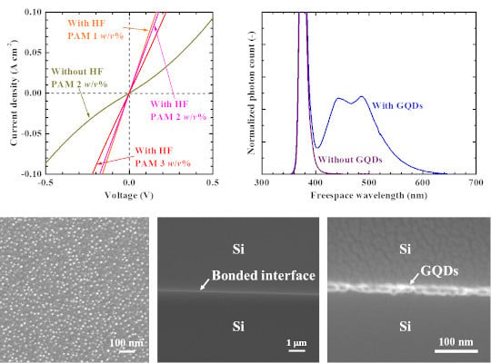
3.1. Bonding via Bare GQDs

First, we present the results of the bonding approach: (1) namely, bond formation via directly coating the colloidal GQD solution onto the semiconductor wafers. Figure 1a shows a plane-view scanning electron microscope image of the GQDs on a Si wafer. The samples for observation were lightly coated with Au via sputtering to prevent electric charge-up during electron microscopy. It was observed that the GQDs, with diameters and an areal density of approximately 10–20 nm and 8 × 1010 cm−2, respectively, were uniformly dispersed on the Si wafer before bonding. Figure 1b shows a cross-sectional image, which was taken by a regular scanning electron microscope detecting secondary electrons, of the bonded interface, for a sample bonded at 300 °C with HF surface pretreatment. The Si wafers are uniformly and firmly intact, with sufficient endurance during the cleaving process, as shown in the figure. Figure 1c shows a magnified view of the bonded interface of Figure 1b. An ensemble of GQDs is stably confined at the interface of the bonded pair Si wafers, thereby forming a Si/GQDs/Si double heterostructure, as shown in the figure.
Figure 2 shows typical current–voltage characteristics across the bonded interfaces for various bonding conditions. The ohmic electrical property, which is suitable for device applications, was obtained for the bonding conditions with HF surface pretreatment, as observed in the straight current–voltage curves. We observed that the samples bonded at 300 °C, the central bonding temperature, with and without HF surface pretreatment exhibited interfacial electrical resistivities of approximately 1 and 20 Ω·cm2, respectively. This result indicates that the HF surface pretreatment provides significantly higher interfacial electrical conductivity, which can be attributed to the removal of the electrically insulating native oxide layer of SiO2 on the Si wafer surface via the HF solution. The higher interfacial electrical conductivity is preferable for most device applications; and therefore, we focused on the bonding with HF pretreatment. Figure 3 plots the dependence of the interfacial electrical resistivity on the bonding temperature for the samples with HF surface pretreatment. It should be noted that the current–voltage data (such as that in Figure 2) includes all series resistances through the sample. Hence, we independently determined the contact resistance of the metal electrode/semiconductor interfaces while using the transmission line method, and then determined the nominal resistivity at the bonded interface by subtracting it from the slope of the current–voltage curve. A minimum interfacial resistivity is observed in terms of the bonding temperature, as shown in Figure 3. This behavior can be attributed to the trade-off between more stable bond formation and GQD or Si oxidation at higher temperatures. As the highest interfacial electrical conductivity measured, we obtained an interfacial resistivity of 0.26 Ω·cm2 for the bonding temperature of 300 °C, while the plots in Figure 3 show the average values for each bonding temperature. Such a high interfacial electrical conductance value is considered as being highly preferable for most optoelectronic device applications, such as solar cells [37,38].
Figure 4 shows the dependence of the interfacial mechanical bonding strength on the bonding temperature for the samples with HF surface pretreatment. No bonding was formed or the bonding strengths were lower than our detection limit with respect to the bonded samples at room temperature. Figure 4 clearly indicates that the increase in bonding temperature increases the interfacial mechanical stability. The bonding temperatures at or above 300 °C were observed to provide sufficient interfacial mechanical stability for practical device applications. With respect to the highest data measured, we obtained an interfacial mechanical strength of up to 340 kPa for the bonding temperature of 300 °C, while the plots in Figure 4 show the average values for each bonding temperature. In addition, the optical property of wavelength conversion was observed as severely degraded for the bonded glass samples that were prepared for the optical measurement for approach (1), and this is presumably due to the aggregation of GQDs during the drying out of the solution [39].

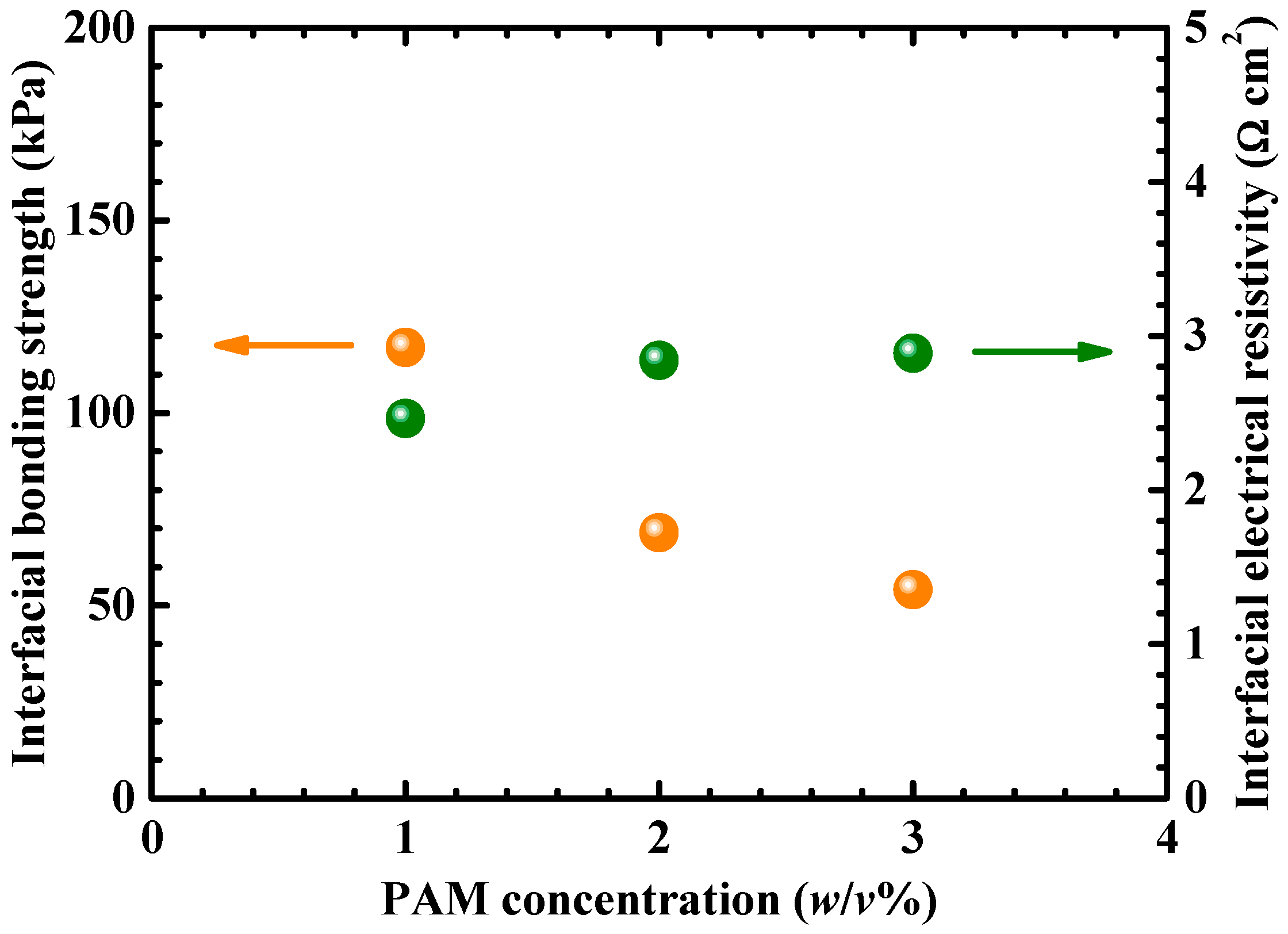
3.2. Bonding via Embedding GQDs in Hydrogel

Second, we present the results for approach (2), wherein we perform bonding by embedding GQDs in a hydrogel material. Figure 5 shows typical current–voltage characteristics across the bonded interfaces for various bonding conditions. In a manner that is similar to the case of the bonding approach (1), the ohmic electrical property was obtained for the bonding conditions with HF surface pretreatment. Figure 6 shows the dependence of the interfacial mechanical bonding strength and electrical resistivity on the PAM concentration for the samples with HF surface pretreatment bonded at room temperature. It is noted that the employment of hydrogel can enable mechanically stable bond formation at room temperature [40,41,42], which was conversely difficult in the case of the bonding approach (1). The hydrogen bonds stemming from PAM presumably causes adhesion to semiconductor surfaces [43,44]. Specifically, hydrogen bonds can form between the -NH2 groups of PAM and the Si surface terminated by the -OH groups due to the water contained in PAM [43]. In addition, the PAM matrix holds the GQDs and suppresses their sedimentation owing to its viscosity induced by the entanglement of PAM polymer chains. Other hydrogel materials, such as agarose and polyvinyl alcohol, may also be used as bonding agents [42]. The interfacial bonding mechanical strength was observed to gradually decrease when the PAM concentration increases, which is potentially attributed to the spatial non-uniformity of the PAM at the bonded interface due to the increased viscosity of the PAM solution, as shown in Figure 6. As the highest data measured, we obtained an interfacial mechanical strength of up to 350 kPa for the case without the HF pretreatment, a PAM concentration of 3 w/v %, and bonding at room temperature.
With respect to the interfacial electrical conductivity, in a manner that is similar to the case of the bonding approach (1), the HF surface pretreatment was observed to reduce the resistivity from approximately 10 Ω·cm2 to 3 Ω·cm2 on average. Nevertheless, the PAM concentration does not significantly affect the interfacial electrical conductivity, as shown in Figure 6. As the highest interfacial electrical conductivity measured, we obtained an interfacial resistivity of 0.53 Ω·cm2 for the case with HF pretreatment, a PAM concentration of 1 w/v %, and bonding at room temperature, while the plots in Figure 6 show the average values for each condition. The realization of this level of electrical conductivity is considered to be preferable for many optoelectronic device applications, such as solar cells [37,38]. PAM, a hydrophilic polymer material, can contain water, and the water-originated ions act as electrical carriers to induce electrical conductance [44]. Reference 42 discusses the influence of the presence of water in the hydrogel on electronic component fabrication and characteristics.
In contrast to approach (1), no degradation was observed in the optical property, even after the dry out of the samples for bonding approach (2), due to the use of the hydrogel material. This result can be potentially attributed to the effects of the surface passivation and/or aggregation suppression of the GQDs [39,45]. Figure 7 shows the photoluminescence spectra of the bonded glass samples with and without GQDs. The mild twin peaks that were observed around 440 and 490 nm were presumably due to possible bimodal size distribution of the GQDs. The change in the spectrum of the photon count in Figure 7 verifies that the GQDs embedded in the bonded interface converts the incident light peaking at approximately 380 nm into another bundle of light peaking at approximately 450–500 nm. This type of optical wavelength conversion can be utilized in applications involving solar cells, where the interfacial GQDs absorb ultraviolet light (380 nm) and emit visible light (450–500 nm) to fit the solar spectral irradiance to the crystalline silicon absorption spectral sensitivity. However, the proposed GQD-bonding scheme can be used, irrespective of the material species. Hence, the most suitable combination of semiconductors can be selected on demand for each application. The tunability of the absorption and emission wavelengths via the quantum-dot size is advantageous for the adjustment of each application. Moreover, the use of an ensemble of dots with a size distribution can fit some of the applications, such as photovoltaics, in response to the broad solar spectrum. In this study, we demonstrated photonic down conversion by GQD, but not up conversion. However, with down conversion, the implementation of an efficient GQD-mediated interface in a multijunction solar cell might not be trivial because it would require a relatively large separation in the bandgap energies between the top and bottom subcells, such as that in an (Al) (In)GaN–Si combination. In contrast, up-converting GQDs [32,33,34] could be more beneficial in such an application. For two-dimensional graphene sheets, albeit not quantum dots, we previously developed graphene-mediated semiconductor wafer bonding to form a Si/graphene/Si double heterostructure [46]. Hence, we demonstrated the preparation of two types of graphene-based-material-cored double heterostructures that can provide a basis for high-performance nanophotonic devices in the future.

4. Conclusions

In the study, we proposed and experimentally demonstrated a semiconductor bonding scheme, which was mediated by GQDs. We investigated two approaches as methods for introducing interfacial GQDs, namely bond formation via directly coating the colloidal GQD solution onto the semiconductor wafers and bonding via GQDs embedded in a hydrogel material. For both cases, we analyzed the dependence of the interfacial mechanical bonding strength and electrical conductivity on bonding conditions, and obtained those sufficient for practical device applications. The use of hydrogel as a matrix agent provided stable bond formation at room temperature. We observed a clear optical wavelength conversion by GQDs at the semiconductor interface, and this can lead to various applications for photon management in integrated devices. The process technique simultaneously allows for bonding formation and interfacial function generation, thereby leading to efficient device production. The proposed bonding scheme can also provide a pathway to fabricate highly efficient double heterostructured optoelectronic devices, which employ GQDs as emitters or absorbers, such as light-emitting diodes [47,48,49], lasers, optical amplifiers, modulators, photodetectors, and solar cells.

Author Contributions

Conceptualization, K.T.; methodology, K.N., K.K. and K.T.; validation, K.N.; formal analysis, K.N.; investigation, K.N. and K.T.; resources, K.T.; data curation, K.N. and K.T.; writing—original draft preparation, K.N. and K.T.; writing—review and editing, K.N., K.K. and K.T.; visualization, K.N. and K.T.; supervision, K.T.; project administration, K.T.; funding acquisition, K.T. All authors have read and agreed to the published version of the manuscript.

Funding

This research was funded by the Fujikura Foundation, the Kato Foundation for Promotion of Science, the Murata Science Foundation, and the Japan Society for the Promotion of Science (JSPS).

Conflicts of Interest

The authors declare no conflict of interest. The funders had no role in the design of the study; in the collection, analyses, or interpretation of data; in the writing of the manuscript, or in the decision to publish the results.

References

  1. Arakawa, Y.; Sakaki, H. Multidimensional quantum well laser and temperature dependence of its threshold current. Appl. Phys. Lett. 1982, 40, 939–941. [Google Scholar] [CrossRef]
  2. Tessler, N.; Medvedev, V.; Kazes, M.; Kan, S.; Banin, U. Efficient near-infrared polymer nanocrystal light-emitting diodes. Science 2002, 295, 1506–1508. [Google Scholar] [CrossRef] [PubMed]
  3. Talapin, D.V.; Murray, C.B. PbSe nanocrystal solids for n- and p-channel thin film field-effect transistors. Science 2005, 310, 86–89. [Google Scholar] [CrossRef] [PubMed] [Green Version]
  4. Tanabe, K.; Nomura, M.; Guimard, D.; Iwamoto, S.; Arakawa, Y. Room temperature continuous wave operation of InAs/GaAs quantum dot photonic crystal nanocavity laser on silicon substrate. Opt. Express 2009, 17, 7036–7042. [Google Scholar] [CrossRef] [PubMed]
  5. Tanabe, K.; Guimard, D.; Bordel, D.; Arakawa, Y. High-efficiency InAs/GaAs quantum dot solar cells by metalorganic chemical vapor deposition. Appl. Phys. Lett. 2012, 100, 193905. [Google Scholar] [CrossRef] [Green Version]
  6. Bao, J.; Bawendi, M.G. A colloidal quantum dot spectrometer. Nature 2015, 523, 67–70. [Google Scholar] [CrossRef]
  7. Adinolfi, V.; Sargent, E.H. Photovoltage field-effect transistors. Nature 2017, 542, 324–327. [Google Scholar] [CrossRef]
  8. Won, Y.-H.; Cho, O.; Kim, T.; Chung, D.-Y.; Kim, T.; Chung, H.; Jang, H.; Lee, J.; Kim, D.; Jang, E. Highly efficient and stable InP/ZnSe/ZnS quantum dot light-emitting diodes. Nature 2019, 575, 634–638. [Google Scholar] [CrossRef]
  9. Ono, K.; Austing, D.G.; Tokura, Y.; Tarucha, S. Current rectification by Pauli exclusion in a weakly coupled double quantum dot system. Science 2002, 297, 1313–1317. [Google Scholar] [CrossRef]
  10. Fujisawa, T.; Hayashi, T.; Tomita, R.; Hirayama, Y. Bidirectional counting of single electrons. Science 2006, 312, 1634–1636. [Google Scholar] [CrossRef] [Green Version]
  11. Schaller, G.; Emary, C.; Kiesslich, G.; Brandes, T. Probing the power of an electronic Maxwell’s demon: Single-electron transistor monitored by a quantum point contact. Phys. Rev. B 2011, 84, 085418. [Google Scholar] [CrossRef] [Green Version]
  12. Tanabe, K. Coupled-double-quantum-dot environmental information engines: A numerical analysis. J. Phys. Soc. Jpn. 2016, 85, 064003. [Google Scholar] [CrossRef]
  13. Sun, H.; Wu, L.; Wei, W.; Qu, X. Recent advances in graphene quantum dots for sensing. Mater. Today 2013, 16, 433–442. [Google Scholar] [CrossRef]
  14. Minati, L.; Del Piano, A. Facile synthesis of water-soluble, highly-fluorescent graphene quantum dots from graphene oxide reduction for efficient cell labelling. C J. Carbon Res. 2019, 5, 77. [Google Scholar] [CrossRef] [Green Version]
  15. Yan, Y.; Gong, J.; Chen, J.; Zeng, Z.; Huang, W.; Pu, K.; Liu, J.; Chen, P. Recent advances on graphene quantum dots: From chemistry and physics to applications. Adv. Mater. 2019, 31, 1808283. [Google Scholar] [CrossRef]
  16. Liu, D.; Chen, X.; Hu, Y.; Sun, T.; Song, Z.; Zheng, Y.; Cao, Y.; Cai, Z.; Cao, M.; Peng, L.; et al. Raman enhancement on ultra-clean graphene quantum dots produced by quasi-equilibrium plasma-enhanced chemical vapor deposition. Nat. Commun. 2018, 9, 193. [Google Scholar] [CrossRef] [Green Version]
  17. Zhao, S.; Lavie, J.; Rondin, L.; Orcin-Chaix, L.; Diederichs, C.; Roussignol, P.; Chassagneux, Y.; Voisin, C.; Müllen, K.; Narita, A.; et al. Single photon emission from graphene quantum dots at room temperature. Nat. Commun. 2018, 9, 3470. [Google Scholar] [CrossRef] [Green Version]
  18. Alferov, Z.I. Nobel lecture: The double heterostructure concept and its applications in physics, electronics, and technology. Rev. Mod. Phys. 2001, 73, 767–782. [Google Scholar] [CrossRef] [Green Version]
  19. Kroemer, H. Nobel lecture: Quasielectric fields and band offsets: Teaching electrons new tricks. Rev. Mod. Phys. 2001, 73, 783–793. [Google Scholar] [CrossRef]
  20. Mi, Z.; Bhattacharya, P.; Fathpour, S. High-speed 1.3 μm tunnel injection quantum-dot lasers. Appl. Phys. Lett. 2005, 86, 153109. [Google Scholar] [CrossRef]
  21. Lasky, J.B. Wafer bonding for silicon-on-insulator technologies. Appl. Phys. Lett. 1986, 48, 78–80. [Google Scholar] [CrossRef]
  22. Tong, Q.-Y.; Goesele, U.M. Wafer bonding and layer splitting for microsystems. Adv. Mater. 1999, 11, 1409–1425. [Google Scholar] [CrossRef]
  23. Takigawa, R.; Higurashi, E.; Suga, T.; Kawanishi, T. Air-gap structure between integrated LiNbO3 optical modulators and micromachined Si substrates. Opt. Express 2011, 19, 15739–15749. [Google Scholar] [CrossRef]
  24. Matsumoto, K.; Zhang, X.X.; Kishikawa, J.; Shimomura, K. Current-injected light emission of epitaxially grown InAs/InP quantum dots on directly bonded InP/Si substrate. Jpn. J. Appl. Phys. 2015, 54, 030208. [Google Scholar] [CrossRef] [Green Version]
  25. Kang, C.-M.; Lee, J.-Y.; Kong, D.-J.; Shim, J.-P.; Kim, S.-H.; Mun, S.-H.; Choi, S.-Y.; Park, M.-D.; Lee, J.; Lee, D.-S. Hybrid full-color inorganic light-emitting diodes integrated on a single wafer using selective area growth and adhesive bonding. ACS Photon. 2018, 5, 4413–4422. [Google Scholar] [CrossRef]
  26. Van Campenhout, J.; Rojo-Romeo, P.; Regreny, P.; Seassal, C.; Van Thourhout, D.; Verstuyft, S.; Di Cioccio, L.; Fedeli, J.M.; Lagahe, C.; Baets, R. Electrically pumped InP-based microdisk lasers integrated with a nanophotonic silicon-on-insulator waveguide circuit. Opt. Express 2007, 15, 6744–6749. [Google Scholar] [CrossRef] [Green Version]
  27. Tanabe, K.; Watanabe, K.; Arakawa, Y. III-V/Si hybrid photonic devices by direct fusion bonding. Sci. Rep. 2012, 2, 349. [Google Scholar] [CrossRef]
  28. Park, H.; Fang, A.W.; Jones, R.; Cohen, O.; Raday, O.; Sysak, M.N.; Paniccia, M.J.; Bowers, J.E. A hybrid AlGaInAs-silicon evanescent waveguide photodetector. Opt. Express 2007, 15, 6044–6052. [Google Scholar] [CrossRef]
  29. Chen, L.; Dong, P.; Lipson, M. High performance germanium photodetectors integrated on submicron silicon waveguides by low temperature wafer bonding. Opt. Express 2008, 16, 11513–11518. [Google Scholar] [CrossRef]
  30. Tanabe, K.; Fontcuberta i Morral, A.; Atwater, H.A.; Aiken, D.J.; Wanlass, M.W. Direct-bonded GaAs/InGaAs tandem solar cell. Appl. Phys. Lett. 2006, 89, 102106. [Google Scholar] [CrossRef] [Green Version]
  31. Shigekawa, N.; Hara, T.; Ogawa, T.; Liang, J.; Kamioka, T.; Araki, K.; Yamaguchi, M. GaAs/indium tin oxide/Si bonding junctions for III-V-on-Si hybrid multijunction cells with low series resistance. IEEE J. Photovolt. 2018, 8, 879–886. [Google Scholar] [CrossRef]
  32. Shen, J.; Zhu, Y.; Chen, C.; Yang, X.; Li, C. Facile preparation and upconversion luminescence of graphene quantum dots. Chem. Commun. 2011, 47, 2580–2582. [Google Scholar] [CrossRef]
  33. Zhuo, S.; Shao, M.; Lee, S.-T. Upconversion and downconversion fluorescent graphene quantum dots: Ultrasonic preparation and photocatalysis. ACS Nano 2012, 6, 1059–1064. [Google Scholar] [CrossRef]
  34. Zhu, S.; Zhang, J.; Tang, S.; Qiao, C.; Wang, L.; Wang, H.; Liu, X.; Li, B.; Li, Y.; Yu, W.; et al. Surface chemistry routes to modulate the photoluminescence of graphene quantum dots: From fluorescence mechanism to up-conversion bioimaging applications. Adv. Funct. Mater. 2012, 22, 4732–4740. [Google Scholar] [CrossRef]
  35. Ge, J.; Lan, M.; Zhou, B.; Liu, W.; Guo, L.; Wang, H.; Jia, Q.; Niu, G.; Huang, X.; Zhou, H.; et al. A graphene quantum dot photodynamic therapy agent with high singlet oxygen generation. Nat. Commun. 2014, 5, 4596. [Google Scholar] [CrossRef] [Green Version]
  36. Kishibe, K.; Hirata, S.; Inoue, R.; Yamashita, T.; Tanabe, K. Wavelength-conversion-material-mediated semiconductor wafer bonding for smart optoelectronic interconnects. Nanomaterials 2019, 9, 1742. [Google Scholar] [CrossRef] [Green Version]
  37. Sharps, P.R.; Timmons, M.L.; Hills, J.S.; Gray, J.L. Wafer bonding for use in mechanically stacked multi-bandgap cells. In Proceedings of the 26th IEEE Photovolt. Specialists Conference, Anaheim, CA, USA, 29 September–3 October 1997; pp. 895–898. [Google Scholar] [CrossRef]
  38. Yoshidomi, S.; Furukawa, J.; Hasumi, M.; Sameshima, T. Mechanical stacking multi junction solar cells using transparent conductive adhesive. Energy Procedia 2014, 60, 116–122. [Google Scholar] [CrossRef] [Green Version]
  39. Sun, M.; Qu, S.; Hao, Z.; Ji, W.; Jing, P.; Zhang, H.; Zhang, L.; Zhao, J.; Shen, D. Towards efficient solid-state photoluminescence based on carbon-nanodots and starch composites. Nanoscale 2014, 6, 13076–13081. [Google Scholar] [CrossRef] [Green Version]
  40. Yuk, H.; Zhang, T.; Lin, S.; Alberto Parada, G.; Zhao, X. Tough bonding of hydrogels to diverse non-porous surfaces. Nat. Mater. 2016, 15, 190–196. [Google Scholar] [CrossRef] [Green Version]
  41. Wirthl, D.; Pichler, R.; Drack, M.; Kettlguber, G.; Moser, R.; Gerstmayr, R.; Hartmann, F.; Bradt, E.; Kaltseis, R.; Siket, C.M.; et al. Instant tough bonding of hydrogels for soft machines and electronics. Sci. Adv. 2017, 3. [Google Scholar] [CrossRef] [Green Version]
  42. Kishibe, K.; Tanabe, K. Hydrogel-mediated semiconductor wafer bonding. Appl. Phys. Lett. 2019, 115, 081601. [Google Scholar] [CrossRef]
  43. Nam, H.G.; Nam, M.G.; Yoo, P.J.; Kim, J. Hydrogen bonding-based strongly adhesive coacervate hydrogels synthesized using poly(N-vinylpyrrolidone) and tannic acid. Soft Matter 2019, 15, 785–791. [Google Scholar] [CrossRef] [PubMed]
  44. Zhang, Q.; Liu, X.; Duan, L.; Gao, G. Ultra-stretchable wearable strain sensors based on skin-inspired adhesive, tough and conductive hydrogels. Chem. Eng. J. 2019, 365, 10–19. [Google Scholar] [CrossRef]
  45. Javanbakht, S.; Namazi, H. Solid state photoluminescence thermoplastic starch film containing graphene quantum dots. Carbohydr. Polym. 2017, 176, 220–226. [Google Scholar] [CrossRef]
  46. Naito, T.; Tanabe, K. Fabrication of Si/graphene/Si double heterostructures by semiconductor wafer bonding towards future applications in optoelectronics. Nanomaterials 2018, 8, 1048. [Google Scholar] [CrossRef] [Green Version]
  47. Song, S.H.; Jang, M.; Chung, J.; Jin, S.H.; Kim, B.H.; Hur, S.; Yoo, S.; Cho, Y.; Jeon, S. Highly efficient light-emitting diode of graphene quantum dots fabricated from graphite intercalation compounds. Adv. Opt. Mater. 2014, 2, 1016–1023. [Google Scholar] [CrossRef]
  48. Kumar, G.S.; Thupakula, U.; Sarkar, P.K.; Acharya, S. Easy extraction of water-soluble graphene quantum dots for light emitting diodes. RSC Adv. 2015, 5, 27711–27716. [Google Scholar] [CrossRef]
  49. Lee, S.H.; Kim, D.Y.; Lee, J.; Lee, S.B.; Young, H.H.; Kim, Y.; Mun, S.C.; Im, S.H.; Kim, T.; Park, O.O. Synthesis of single-crystalline hexagonal graphene quantum dots from solution chemistry. Nano Lett. 2019, 19, 5437–5442. [Google Scholar] [CrossRef]
Figure 1. (a) Plane-view scanning electron microscope image of the graphene quantum dots (GQDs) on a Si wafer; (b) Cross-sectional scanning electron microscope image of the bonded interface, for the sample with wet hydrofluoric (HF) surface pretreatment bonded at 300 °C for bonding approach (1); and, (c) Magnified view of the bonded interface of (b).
Carbon 06 00028 g001
Figure 2. Current–voltage characteristics across the bonded interfaces with HF surface pretreatment bonded at 100, 300, and 500 °C, and without HF surface pretreatment bonded at 300 °C for bonding approach (1).
Carbon 06 00028 g002
Figure 3. Dependence of the interfacial electrical resistivity on bonding temperature for the samples with HF surface pretreatment for bonding approach (1).
Carbon 06 00028 g003
Figure 4. Dependence of the interfacial mechanical bonding strength on bonding temperature for the samples with HF surface pretreatment for bonding approach (1).
Carbon 06 00028 g004
Figure 5. Current–voltage characteristics across the bonded interfaces with HF surface pretreatment bonded at room temperature with polyacrylamide (PAM) concentrations corresponding to 1, 2, and 3 w/v %, and without HF surface pretreatment bonded at room temperature with a PAM concentration of 2 w/v % for bonding approach (2).
Carbon 06 00028 g005
Figure 6. Dependences of the interfacial mechanical bonding strength and electrical resistivity on PAM concentration for the samples with HF surface pretreatment bonded at room temperature for bonding approach (2).
Carbon 06 00028 g006
Figure 7. Photoluminescence spectra of the bonded glass samples with and without GQDs for bonding approach (2).
Carbon 06 00028 g007

