Review

A Library of Doped-Graphene Images via Transmission Electron Microscopy

by
Phuong Viet Pham
1,2
1
SKKU Advanced Institute of Nano Technology (SAINT), Sungkyunkwan University (SKKU), Suwon, Gyeonggi-do 440-746, Korea
2
Center for Multidimensional Carbon Materials, Institute for Basic Science, Ulsan 44919, Korea
Submission received: 21 April 2018 / Revised: 15 May 2018 / Accepted: 23 May 2018 / Published: 28 May 2018
(This article belongs to the Special Issue Transmission Electron Microscopy and Carbon Materials)

Abstract

:
Much recent work has focused on improving the performance of graphene by various physical and chemical modification approaches. In particular, chemical doping of n-type and p-type dopants through substitutional and surface transfer strategies have been carried out with the aim of electronic and band-gap tuning. In this field, the visualization of (i) The intrinsic structure and morphology of graphene layers after doping by various chemical dopants, (ii) the formation of exotic and new chemical bonds at surface/interface between the graphene layers and the dopants is highly desirable. In this short review, recent advances in the study of doped-graphenes and of the n-type and p-type doping techniques through transmission electron microscopy (TEM) analysis and observation at the nanoscale will be addressed.

1. Introduction

Graphene, a honeycomb sp2-bonded carbon atom lattice, shows new physical characteristics such as ambipolar field effect [1,2,3,4,5,6,7,8,9,10,11,12], extreme mobility (200,000 cm2/Vs) [13], or extraordinary quantum Hall effect [14,15] unveiling great applications in graphene nanoribbon (GNR) transistor, gas sensor, supercapacitor, transparent conducting electrode, field-effect transistor (FET), and silicon complementary metal oxide semiconductor (CMOS)-based logic circuit. Doping based on wet chemical and dry plasma methods is one of the best method for tailoring and tuning the electrical properties, band-gap, and work function of graphene.
Although pristine graphene shows ambipolar field effect, it is not sensitive and air-stable to surrounding weak doping [16] or to polymer residues utilized in the fabrication of devices. Thereby, the controlled chemical doping with holes or electrons or reducing surface contaminations in modulating the electronic properties of graphene become very important and necessary. In principle, doping on semiconductors is a process that involves local manipulation of its conductivity and charge density, and it is one of the main modification and modulation strategies in micro- and nano-electronics. The abundant doping strategies have been completely demonstrated on transition metal dichalcogenide (e.g., MoS2) [17]. In general, the dopant donates electrons to graphene at ambient environment (named donor or n-type dopant), or it accepts electrons and leaving holes on graphene and then forming covalent bonding (named acceptor or p-type dopant) [6,7].
The TEM is the most sophisticated analysis instrument and a great breakthrough in technology to serve for deeper observing the intrinsic structures of organic and inorganic thin film materials at the nanoscale (10−9 nm). The TEM was discovered by Max Knoll and Ernest Ruska in 1931, then awarded the Nobel laureate in physics in 1986. Following the decade-by-decade, the TEM was re-designed and upgraded in engineering and technology for deeper observation and more feasible manipulation. The main parts of TEM for observation missions consist an electron emission source, electromagnetic lenses, and an electron detector. It will interact with the measurement specimen through an electron beam that produced and accelerated, then focused on the specimen by the lenses; the beam will pass through it for modifying and imprinting its images. This review will briefly present the experimental results in recent reports related to the p- and n-type doped graphenes via substitutional doping and surface transfer doping under observations of the TEM analysis instrument.

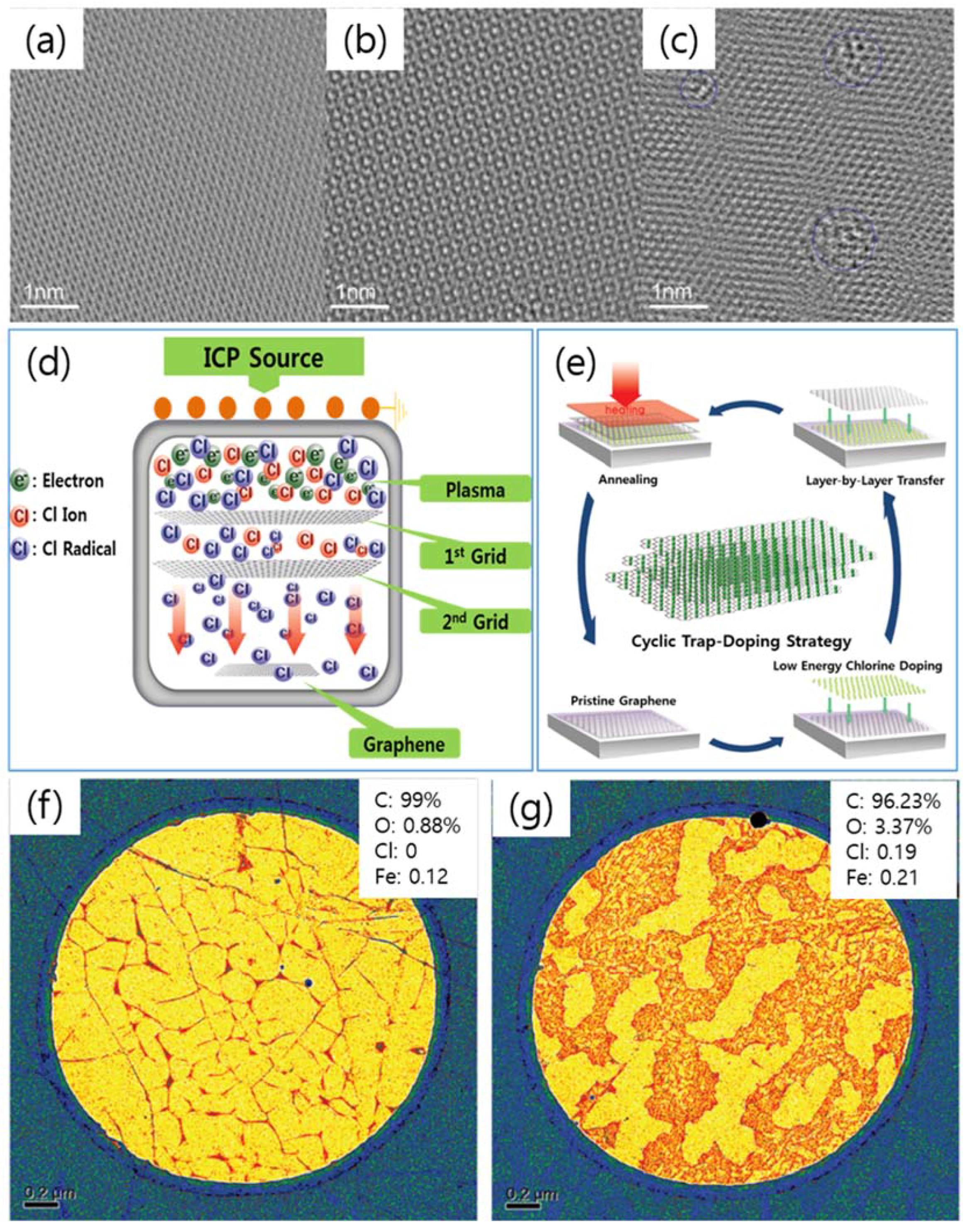
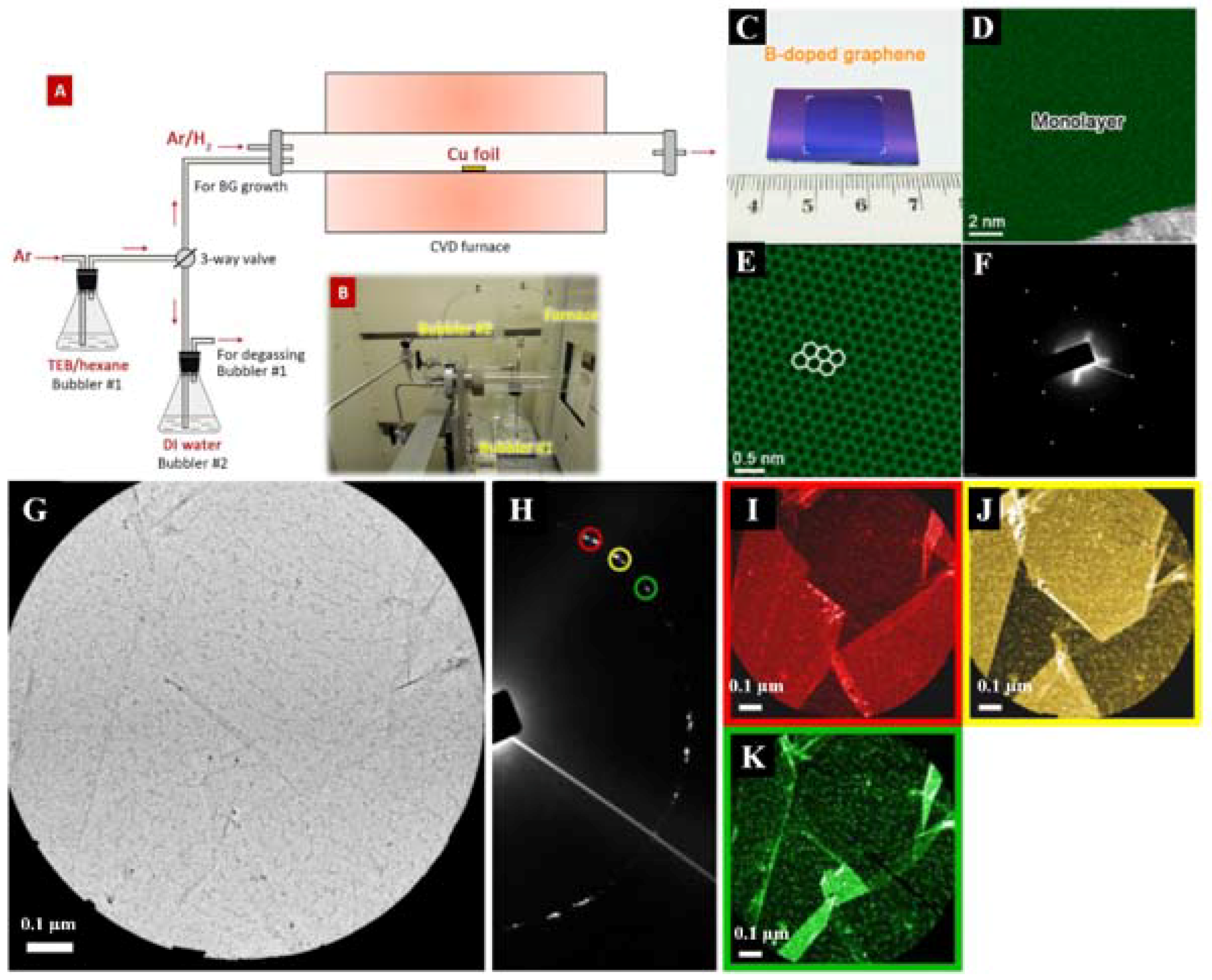
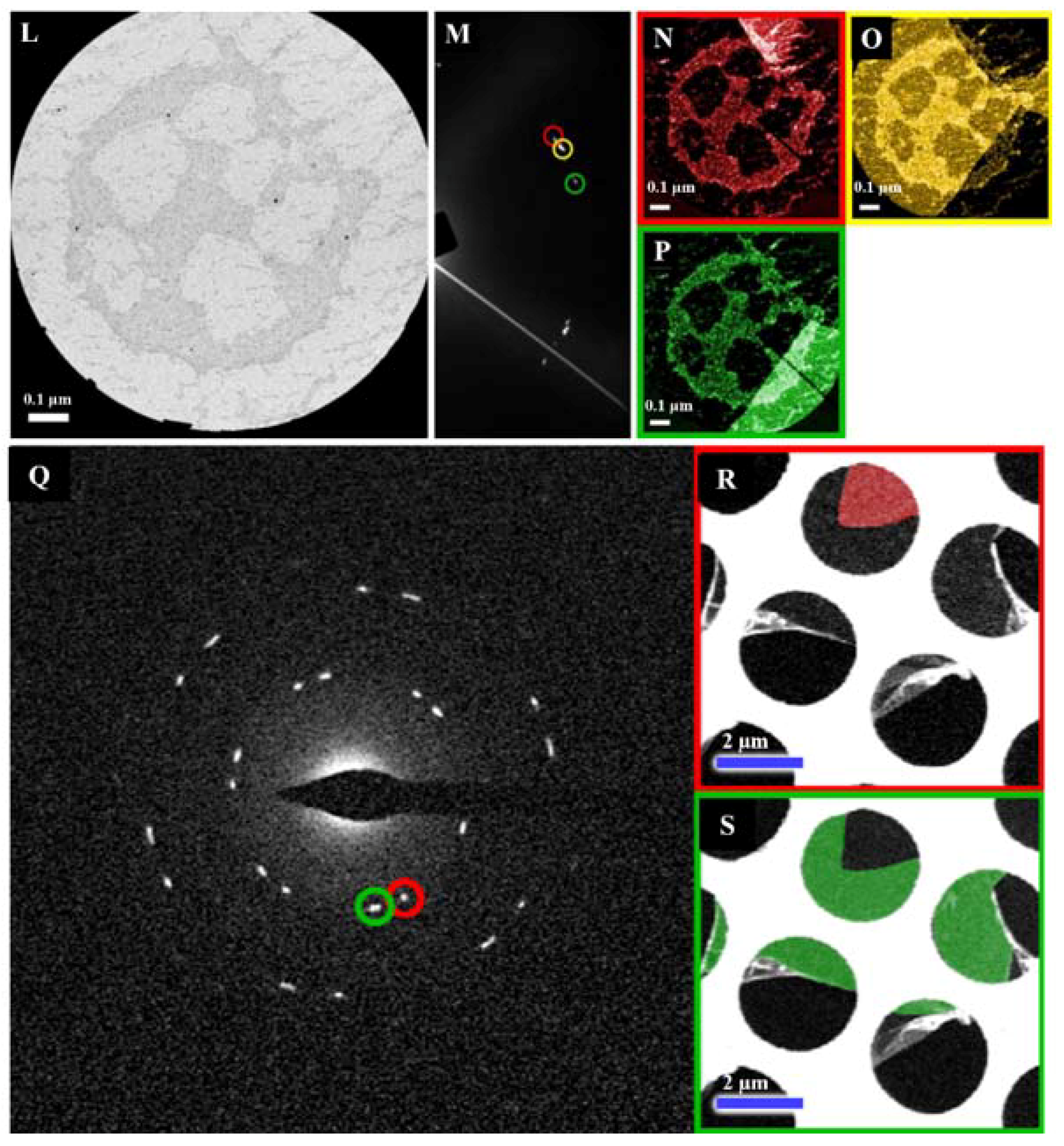
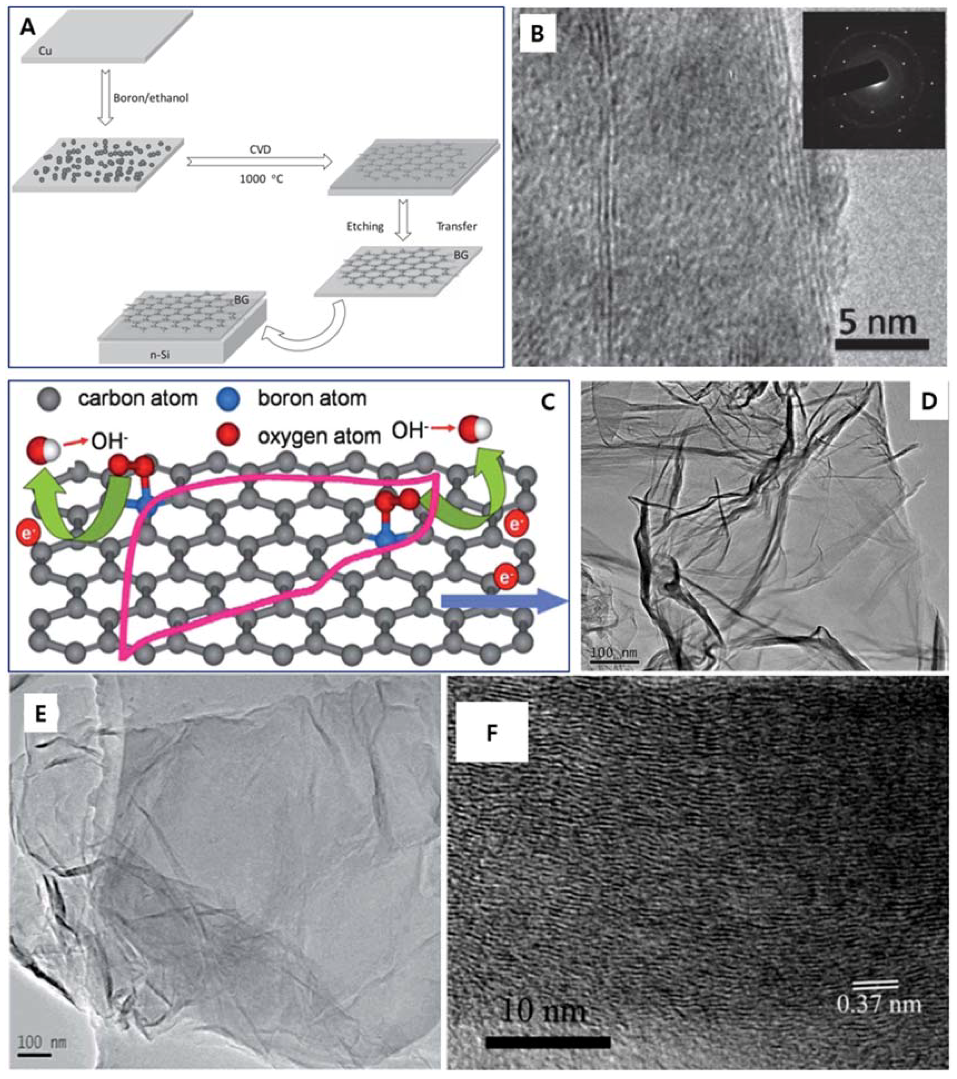
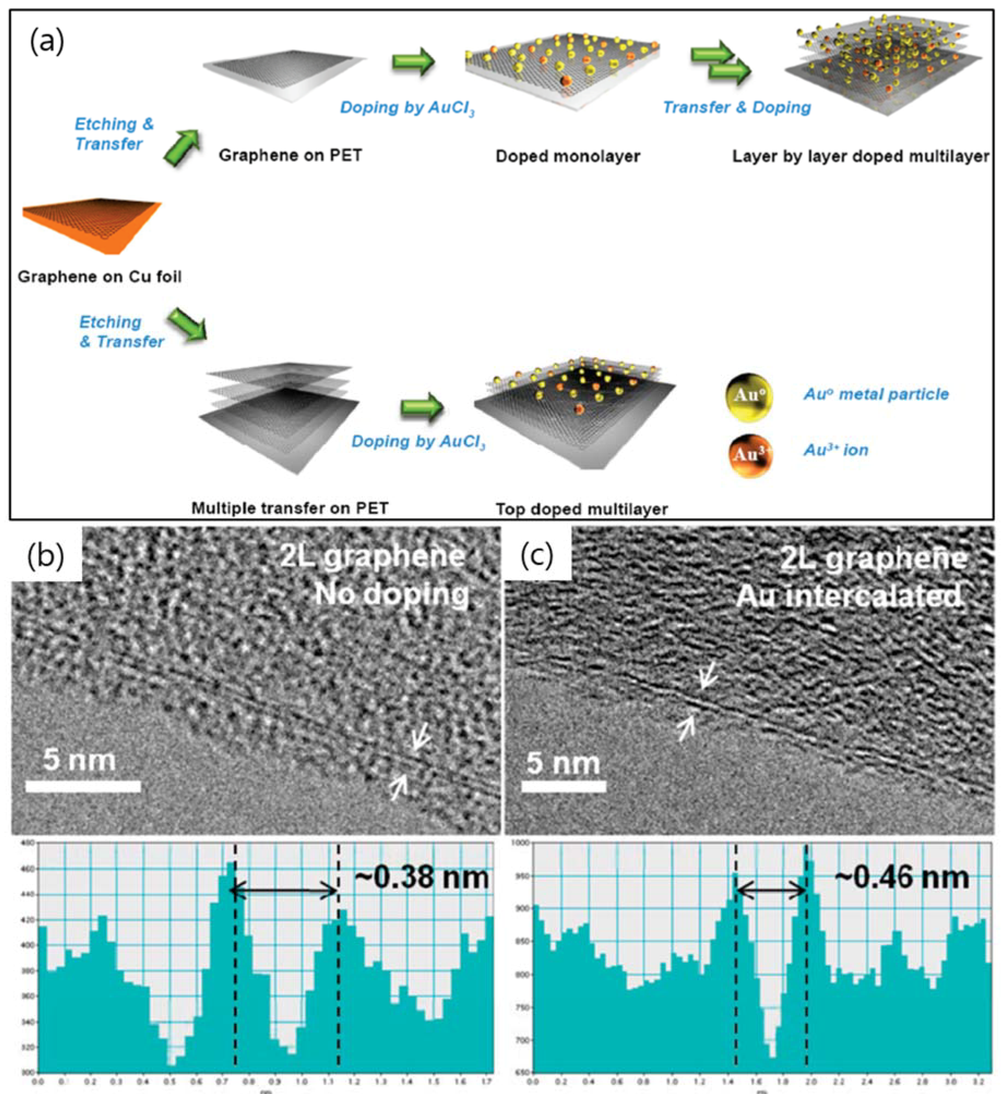
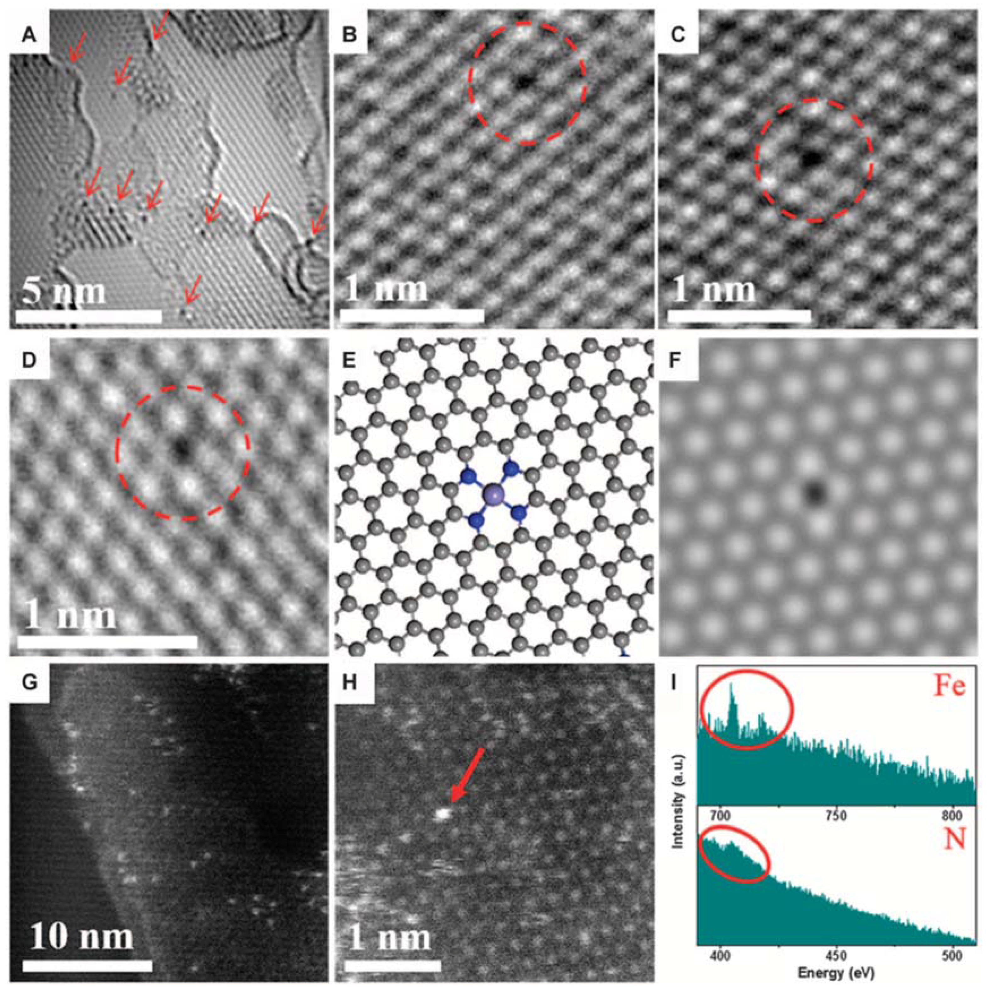
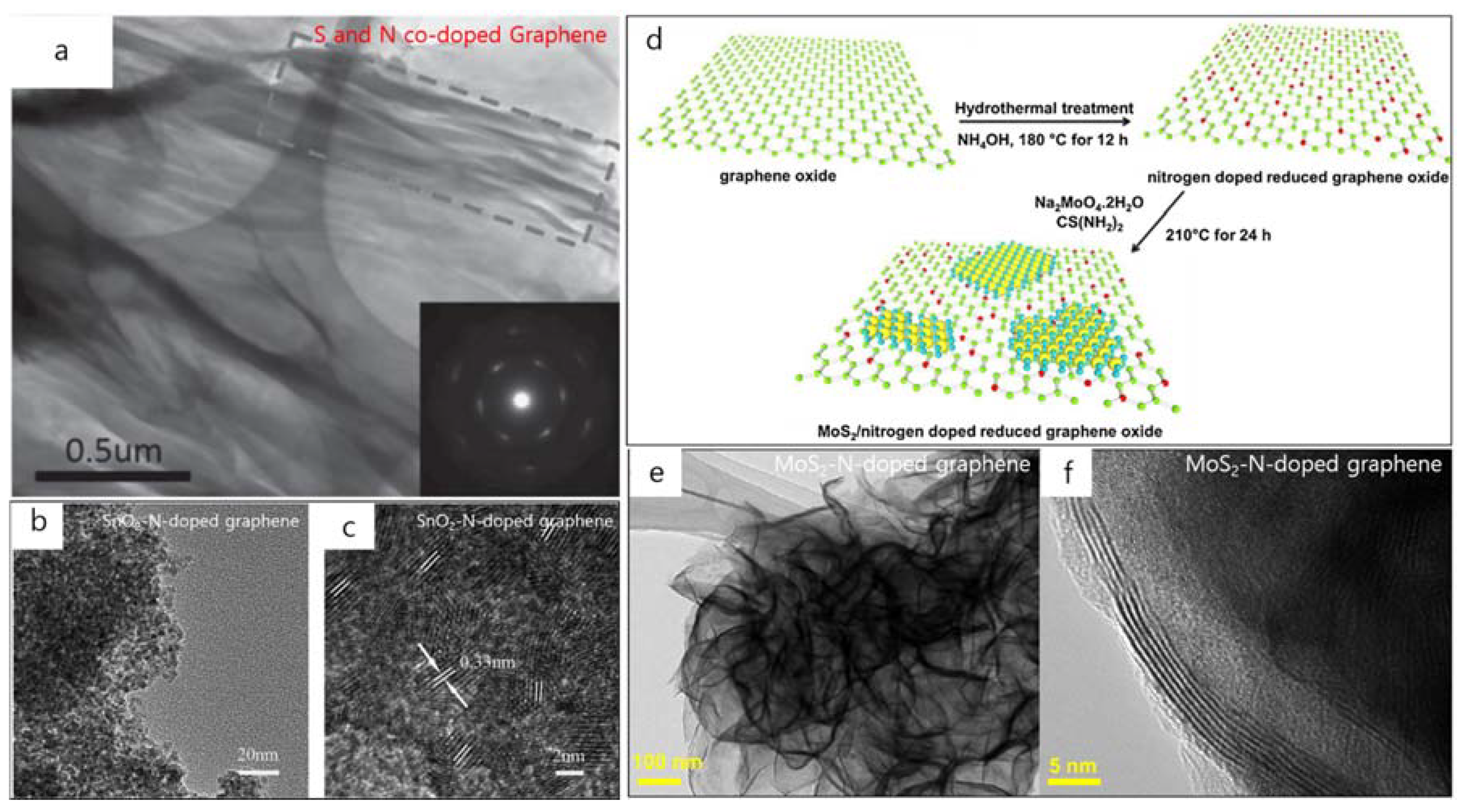
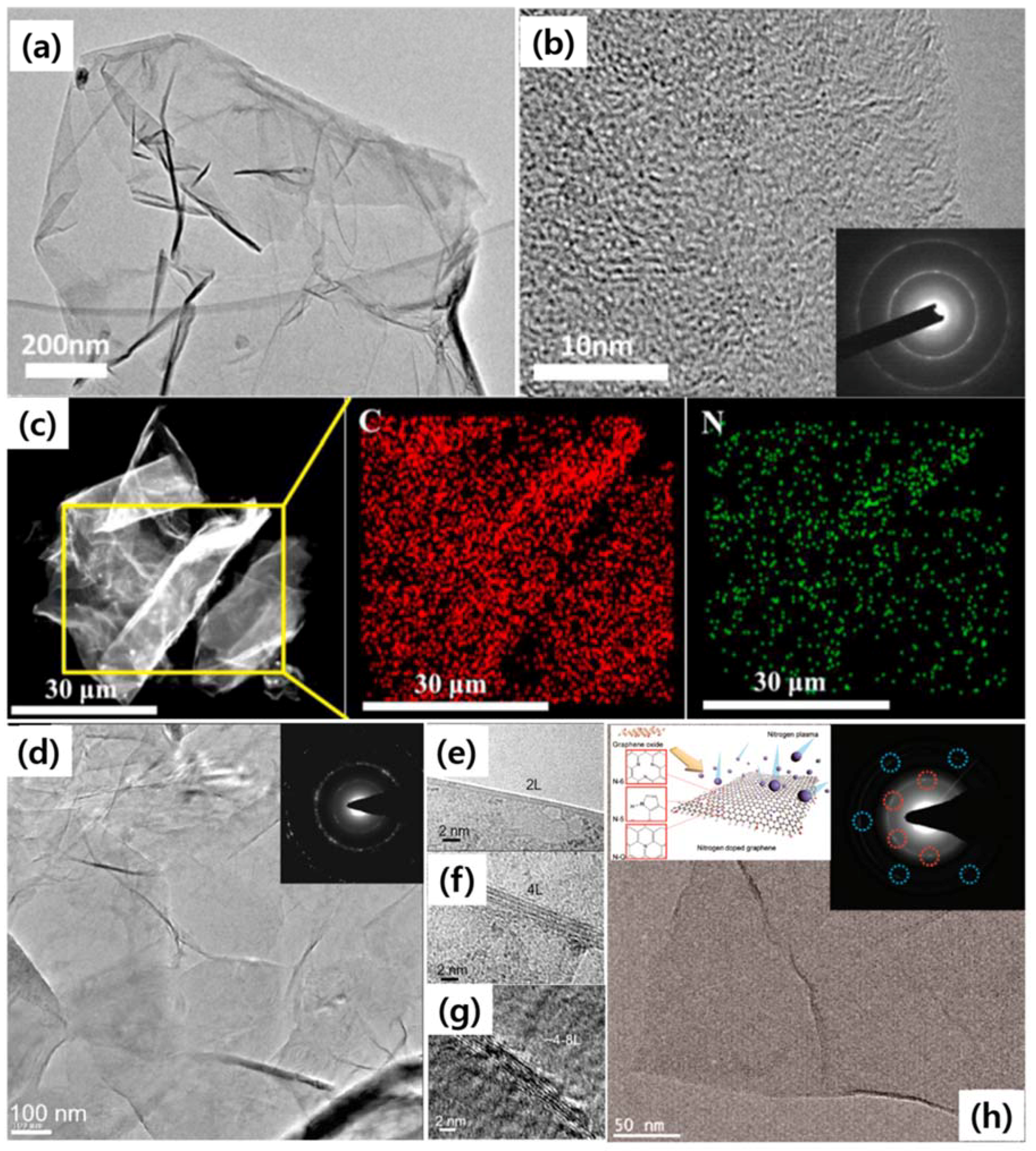
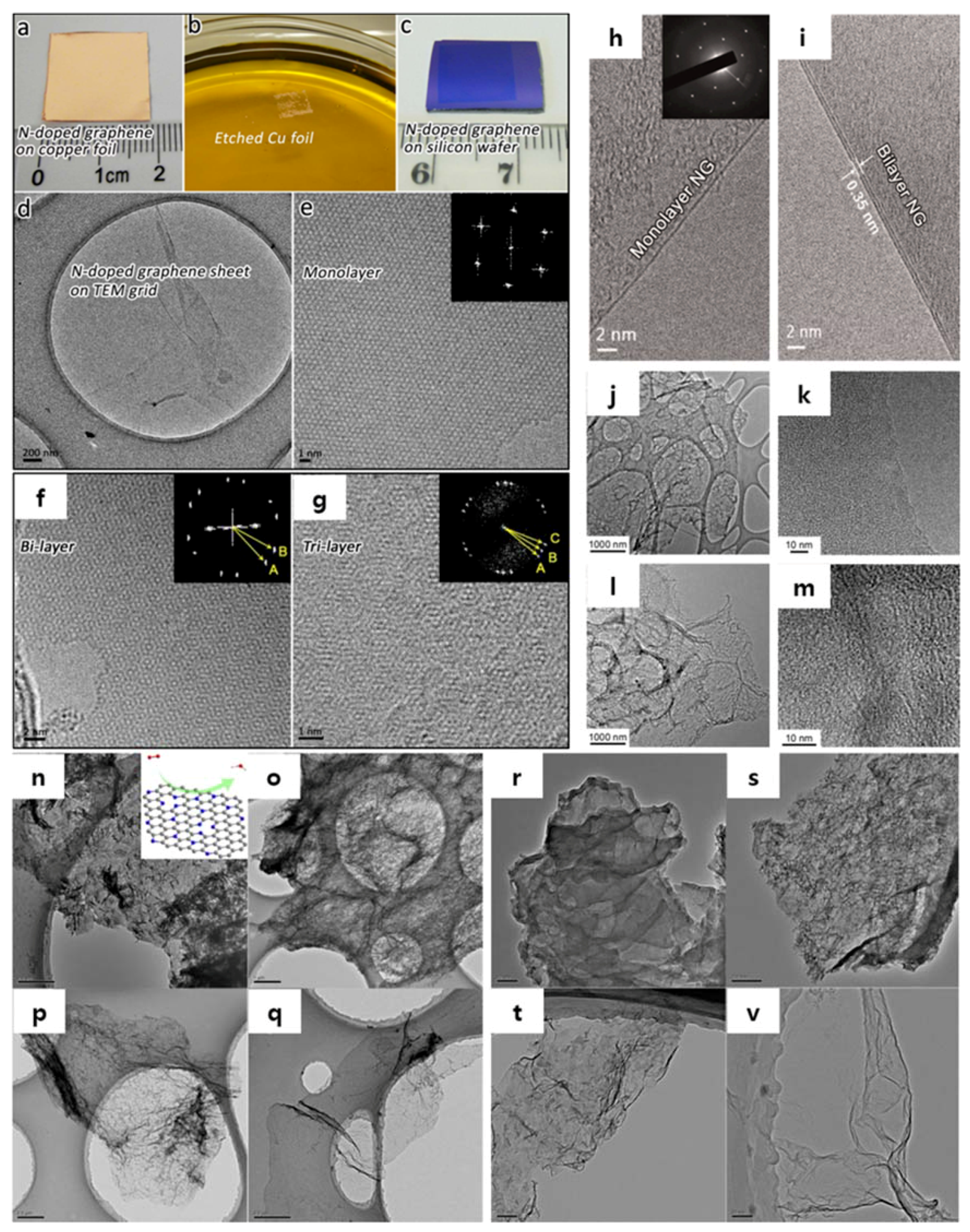
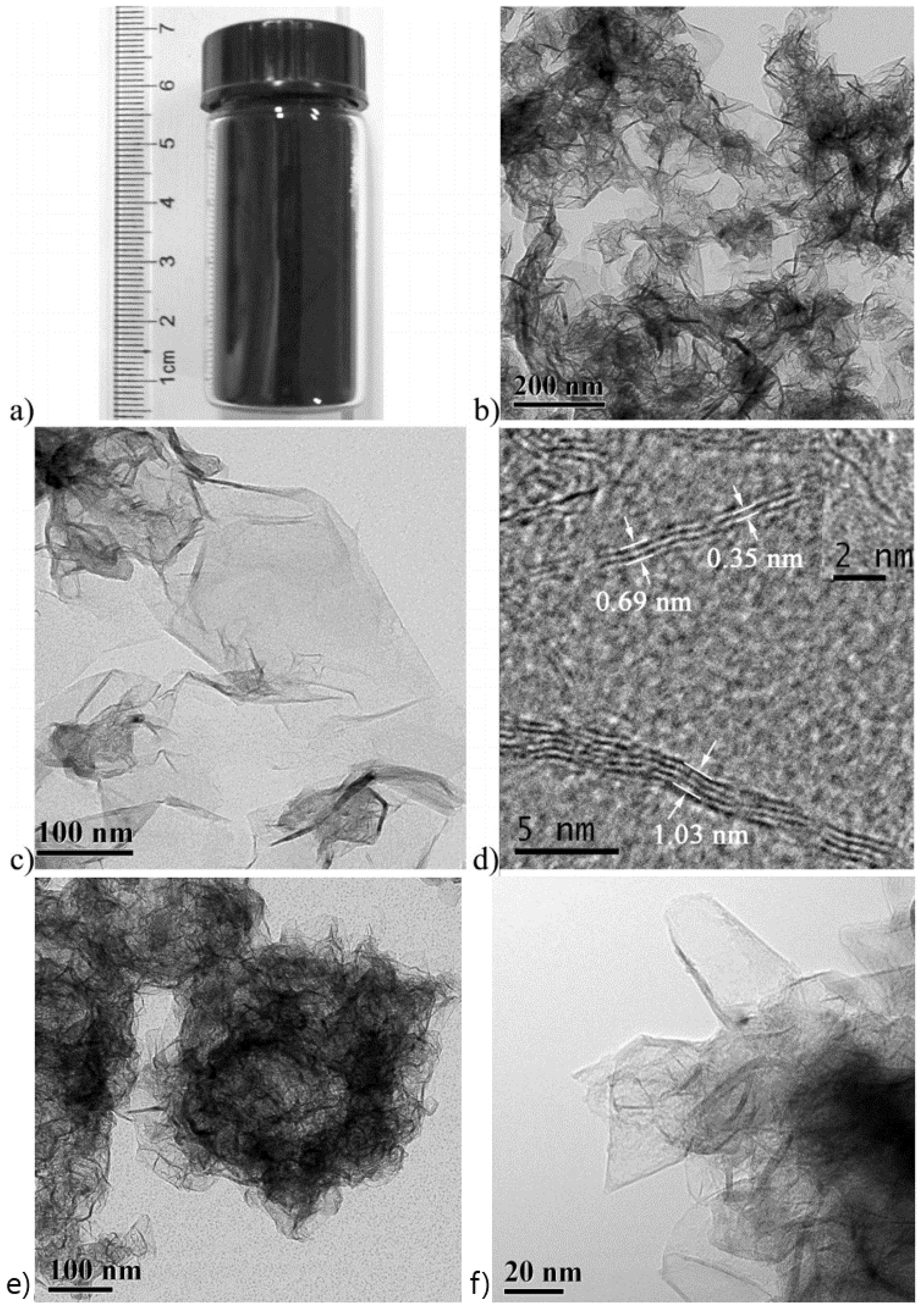
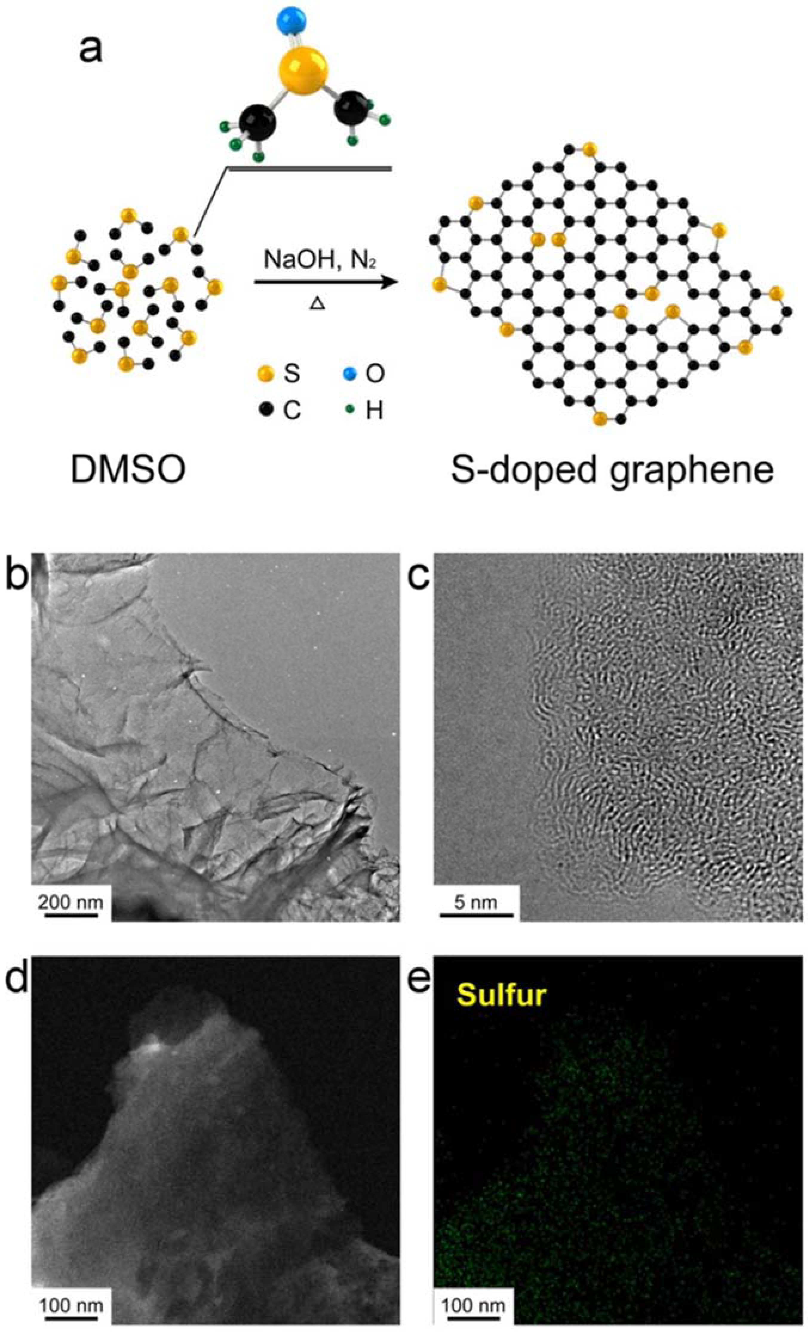
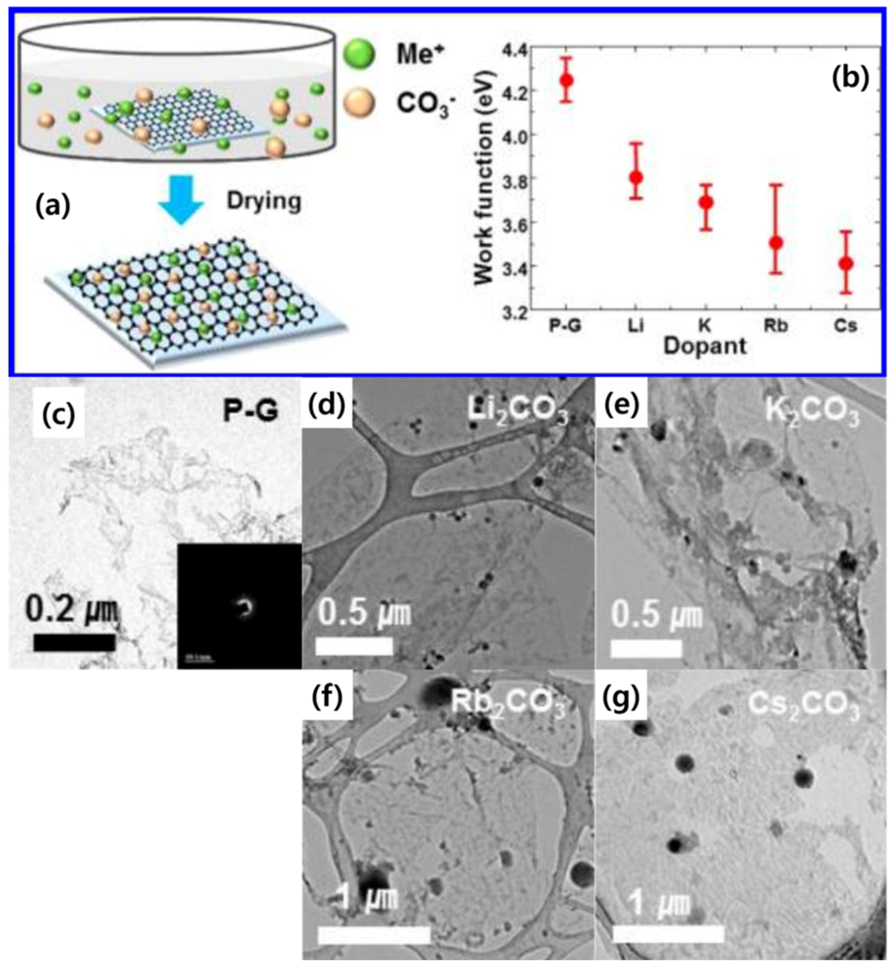
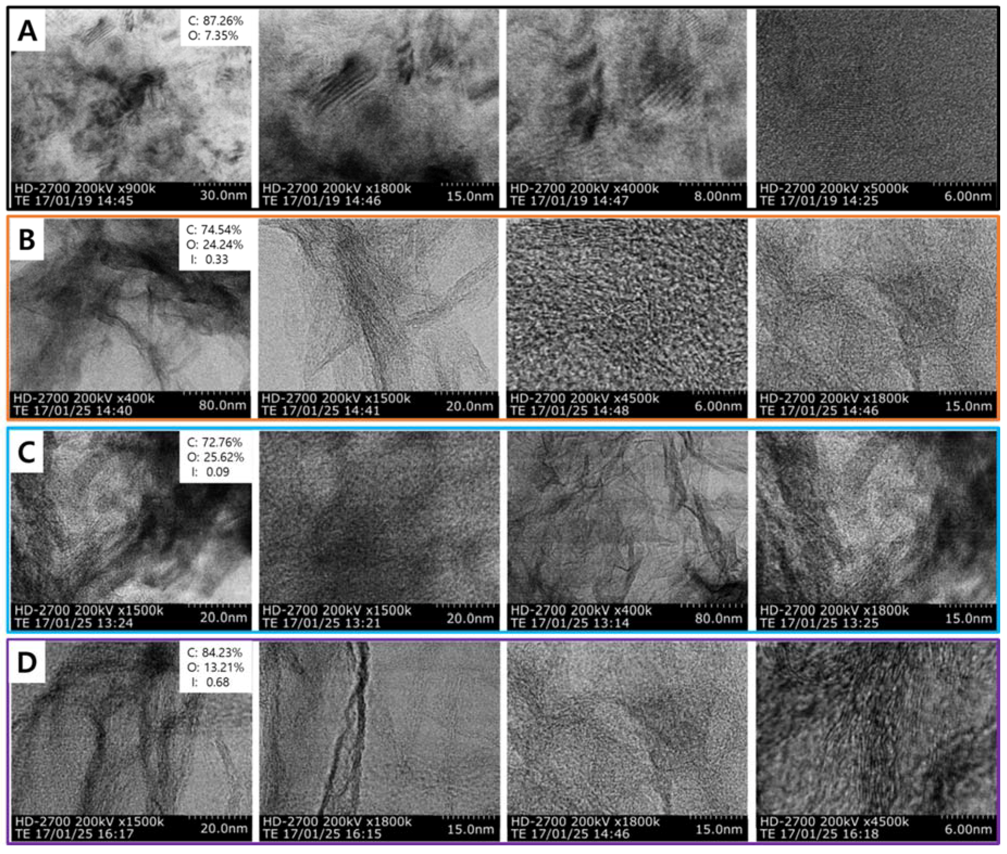
2. TEM Observations of Doped-Graphenes

Recently, the observation of the doped-graphene thin film materials has been well-investigated and great achievements have been made in the image capturing of them at the nanoscale [18,19,20,21,22,23,24,25,26,27,28,29,30,31,32,33,34,35,36,37,38,39,40,41,42,43,44,45,46,47,48,49,50,51,52,53,54,55,56,57,58,59,60,61,62,63,64,65,66,67,68,69,70,71,72,73,74,75,76,77,78,79,80,81,82,83,84,85,86,87,88,89,90,91,92,93,94,95,96]. By the assistances of low-magnification TEM, high-resolution TEM (HR-TEM), spherical aberration-corrected HR-TEM, bright-field TEM (BF-TEM), diffraction-pattern TEM (DP-TEM), dark-field TEM (DF-TEM), scanning transmission electron microscopy (STEM), dark-field scanning transmission electron microscopy (DF-STEM), scanning transmission electron microscopy electron energy loss spectroscopy (STEM_EELS), high-angle annular dark-field scanning transmission electron microscopy (HAADF-STEM), and micro-energy-disperse X-ray spectroscopy in TEM (micro EDS-TEM), the intrinsic structure of thin films was clearly visible at the nanoscale.
In 2011, Wu et al. reported the plasma doping method on graphene and graphene nanoribbons (GNR), utilizing the chlorine (Cl), hydrogen (H2), and fluorine (F2) gases as precursors (Figure 1a–c) [18]. To probe the differences induced by plasma doping with the pristine graphene, the aberration-corrected atomic resolution TEM was carried out. The TEM images of GNRs after 1 min of Cl plasma treatment revealed the same structure with a small disorder (Figure 1b) compared with the pristine graphene (Figure 1a). However, with the increase of the Cl plasma treatment (3 min), the TEM image showed obvious high disorder and defects formed on the GNR surface (Figure 1c), compatible to the Raman spectra which is a high D-band, as shown in this report [18]. The limitation of this report is that the damage still occurs even at low powers and short treatment times.
Similar to Cl plasma doping in Wu et al., Pham et al. explored a new innovation in designing the inductively coupled plasma (ICP) system by inserting the dual mesh-grids between the plasma source and the substrate holder in order to avoid the plasma damage induced on the graphene surface (Figure 1d) [19,20,21,22,23,24]. Consequently, a new damage-free plasma doping strategy was carried out by a multi-layer cyclic trap-doping strategy (Figure 1e) [18,19,20,21,22,23,24]. Using TEM, the location of the Cl atoms in the Cl trap-doped graphene was investigated. Figure 1f,g show the low-magnification color scaled DF-TEM images of a pristine bilayer graphene and low energy Cl radical-trapped bilayer graphene, respectively. The wide brown-colored regions in Figure 1g are the Cl-resided locations between the two graphene layers. The very thin network of brown color in Figure 1f is the slight Cl doping on the graphene, induced by the remaining FeCl3 etchant after being utilized in the wet transfer process. The micro EDS-TEM was demonstrated as further proof for the existence of the Cl-trap effect between the two graphene layers (Insets of Figure 1g,f).
Boron (B) p-type doping is an efficient approach in the modification of the electronic characteristics of graphene and leads to diverse applications [25,26,27,94]. In 2015, Lv et al. fabricated an ultrasensitive gas sensing device through the direct bubbler-assisted atmosphere pressure chemical vapor deposition (BA-APCVD) synthesis of large-scale B-doped graphene, utilizing the triethylborane (TEB)/hexane solution as the precursor (Figure 2A–S) [25]. Figure 2D,E reveals the aberration-corrected medium angle annular DF-STEM images of the pristine B-doped monolayer graphene as the green area. The DF-STEM image (Figure 2E) and the selected-area electron diffraction (SAED) pattern (Figure 2F) show that the hexagonal lattice of the graphene is not disordered with the presence of B-substitutional doping. The DF-TEM technique is able to choose one of the diffraction spots to create the image and, as the result, the grain sizes of the pristine monolayer graphene and B-doped monolayer graphene were observed in Figure 2G–K and Figure 2I–P, respectively. Due to the large size of the objective aperture, some spots are not fully separated. However, most of the grains show clear boundaries, thus, single grains can be easily distinguished. Both pristine monolayer graphene and B-doped monolayer graphene have the grain sizes of 100 nm to >1 μm (Figure 2G–K and Figure 2I–P). By the low-magnification DF-TEM image, a large domain of 7 μm from the B-doped monolayer graphene was seen (Figure 2Q–S). Figure 2Q shows the SAED pattern and Figure 2R,S shows the DF images; the circled diffraction spots in the SAED were used for the DF-TEM imaging. The white part in the DF-TEM is the amorphous carbon mesh of the TEM grid. The color of the border line corresponds to the circle in the SAED of the same color.
Additionally, on the B-doped graphene, Li et al. used B powder and ethanol as doping precursors for the direct CVD synthesis of B-doped multilayer graphene on the Cu substrate at 1000 °C for the fabrication of the graphene-silicon p-n junction solar cell (Figure 3A) [26]. The HR-TEM (Figure 3B) and the DP images (inset of Figure 3B) revealed the multilayer (3–5 layers) and a hexagonal atomic-crystallography structure of the synthesized-B-doped graphene, respectively. Compared to the pristine monolayer graphene, this B-doped multilayer graphene shows a sheet resistance (Rs) of about 1500–2000 Ω/sq and transmittance (%T) of 95.7% at 550 nm, which is well accepted in nanoelectronics [26]. As the result, this B-substitutional doping on graphene could apply to the p-n junction solar cell with a good power conversion efficiency (3.4%) under the air mass of 1.5 [26].
Another catalyst-free approach to synthesize the large-scale B-doped graphene is by the thermal annealing approach of graphite oxide (GO) in the presence of a B2O3 precursor (Figure 3C) [27]. As expected, B atoms from the B2O3 vapor could be doped into a graphene lattice at a high temperature. In the low magnification-TEM image (Figure 3D), the flattened B-doped graphene sheets are randomly stacked together, forming a flake-like structure similar to pristine graphene (Figure 3E). The HR-TEM image shows that the adjacent interlayer distance of the B-doped graphene is 0.37 nm (Figure 3F), which is closer to the crystal plane of graphite (0.335 nm) [97]. Compared to the pristine graphene, the as-synthesized B-doped graphene exhibits novel electrocatalytic activity and high stability towards the oxygen reduction reaction (ORR) in the alkaline electrolyte and is well sustainable to poison in the fuel cells although its mechanism is unclear [27].
An AuCl3 doping strategy intercalated in between of the four layer-by-layer graphenes and on the topmost of the four layers of graphene was found out by Gunes et al. in 2010 (Figure 4a) [28]. Graphene synthesized on Cu is mostly a single layer, just a small portion of the bilayer and the trilayer. HR-TEM images in Figure 4b,c reveal a bilayer graphene structure with a double line without and with the presence of AuCl3. The interlayer distances of the intensity profiles showed for pristine bilayer graphene (~0.38 nm) and Au-intercalated bilayer graphene (~0.46 nm). The interlayer expansion is due to the presence of the Au particle dopant. Consequently, the very good performances of AuCl3 intercalation in the four layers of graphene showed Rs (54 Ω/sq), %T (85%) at 550 nm, and high flexibility (up to 1000 bending cycles on polyethylene terephthalate (PET) substrate) [28]. This work could further improve in performance by reducing the defects during synthesis and wet transfer to achieve a greater requirement for the replacement of indium tin oxide (ITO) in many industrial applications such as OLED, solar cell, flexible display, touch panel, or electronic paper.
Very recently, a new p-type titanium oxide (TiO2) dopant has used to dope on the GO nanocrystal by the hydrothermal method as indicated in the TEM images as shown in Figure 5a–c [31]. The TiO2-doped GO nanocrystals are entangled with each other as scrolled paper. Figure 5b shows the cross-sectional TEM image of TiO2-doped GO. Here, the thickness of the TiO2-doped GO is observed and analyzed about 1–10 nm, which corresponds to 3–9 layers of graphene. Figure 5c shows an HR-TEM image of TiO2-doped GO with a rippled structure around 5 nm. It is obvious proof that transparent and large entangled-GO nanocrystals were observed and the central portion of the TEM image is similar to the graphene plates as the nature of amorphous carbons. By this doping type, a band gap was reduced from 3.1 eV down to 2.36 eV due to the electronic interactions of TiO2 and GO [31].
In 2015, Deng et al. reported one doping method to embed the FeN4 dopant in the graphene sheets by high-energy ball milling of iron phthalocyanine (FePc) whilst keeping the graphene nanosheet (GN) under controllable conditions (Figure 6) [32]. High-energy ball milling is a novel approach to cutting and reconstructing the chemical bonds of the thin materials with controllable input energy. The morphology of FeN4/GN is revealed in Figure 6A–D utilizing the spherical aberration-corrected HR-TEM at a voltage of 80 kV. One could observe the homogeneous dispersed small black dots in graphene. Some could assign the single Fe atoms as red arrows and circles in Figure 6A–D. The structure of the single Fe centers was further defined by the HAADF-STEM images with sub-angstrom resolution (Figure 6G,H). As the result, the atomic size and homogeneous distribution of the bright dots in the graphene network were seen. By EELS atomic spectra of the bright dots (Figure 6I), one could obviously observe the Fe and N elements in one bright dot, suggesting the formation of Fe-Nx bonding. This implies that the Fe atoms observed in Figure 6A–D,G,H should be bonded with N atoms and further contacted to the graphene lattice, as shown in the atomic models (Figure 6E) for the experimental structures (Figure 6D), which is consistent with the density functional theory (DFT)-simulated HR-TEM image (Figure 6F). The Raman data and the X-ray diffraction (XRD) furthers the high-dispersed possibility of Fe in FeN4/GN and is highly compatible with the TEM and HAADF-STEM observations [32]. These discoveries would open a new design way of highly worth catalytic oxidation reaction at low temperatures.
Substitutional doping with B, phosphorus (P), N, or sulfur (S) single atoms in the carbon network could modulate the chemical characteristics, create new active sites, and greatly improve the catalytic activity of graphene [27,33,37,43,77,78,79,80]. In particular, co-doping through the mixture of two or three metal elements with electronegativity could produce a novel electron distribution resulted in a synergistic effect [86]. Recently, S and N co-doping incorporated into graphene sheet was demonstrated by Duan et al. to enhance the metal-free activation of peroxymonosulfate (PMS) for the catalytic oxidation of phenol [34]. Co-doping with S highly upgraded the catalytic efficiency of N-doped graphene (NG) [34]. The morphology and structure of GO and S–N co-doped rGO (SNG) were obtained from TEM images (Figure 7a) [34]. The difference from the smooth surface of GO, silk-like wrinkled flakes, and several stacked layers was observed on SNG (Figure 7a). The wrinkled sheets originated from the reconstruction of graphene during thermal annealing. In the disoriented features of graphene, TEM image also revealed the stacked aggregates of SNG with wrinkled graphene sheets (Figure 7a) and the SAED spot rings can be assigned to the hexagonal carbon lattice structure of graphite planes (inset of Figure 7a). The interlayer spacing was reduced from 0.83 nm (GO) to 0.34 nm (SNG) [34]. During this co-doping process, many O-functional groups would be removed to achieve a higher reducibility, leading to powerful π–π stacking in graphene planes. XRD and X-ray photoelectron spectroscopy (XPS) data also confirmed the changes in the chemical compositions and surface functional groups [34]. Consequently, the S–N co-doped graphene would be a high-performance metal-free catalyst for sustainable environmental remediation.
Another example of co-doping on large-scale graphene was showed by Zhou et al. with SnO2–N co-dopants which were synthesized through a rapid and simple microwave-assisted solvothermal approach with a few minutes of the growth process [35]. SnO2 crystals were densely anchored on N-doped graphene sheets (Figure 7b,c). From the HR-TEM image, the SnO2 nanocrystal has a size of 3 nm and the lattice fringes of 0.33 nm correspond to the (110) planes of tetragonal SnO2 (Figure 7c). It is implied that the SnO2–N co-doped graphene composite possessed both high capacity and cycling characteristics. It is believed that due to the synergistic effect of both the SnO2 nanocrystals and N-doped graphene, this research will save time and provide energy in other metal oxide–N doped graphene syntheses in the future.
In 2016, Lingappan et al. reported a new MoS2/N-co-doped rGO material which was synthesized via a two-step in-situ hydrothermal process to serve as the electrode in Li-ion batteries, as shown in Figure 7d [36]. This co-doping process expects a high improvement of the wettability and electrical transport capability in pristine graphene. The morphology of the MoS2/N-co-doped rGO was analyzed by field emission HR-TEM (Figure 7e,f). The interconnected network formation is believed to arise from the interfacial Mo–N interaction between MoS2 and N-rGO. Thereby, it leads to promote the electrochemistry and stability in this heterostructure. The HR-TEM image (Figure 7f) indicates that the MoS2 sheets consist of 4–7 layers with a lattice spacing of 0.62 nm. This work opens the new creativity of novel functional materials serving as electrodes in Li-ion batteries.
To investigate the ORR, She et al. developed the large-scale N-doped graphene synthesis at 900 °C while expecting a high catalytic activity, novel durability, economic cost for ORR, and high energy density storage in fuel cells and batteries (Figure 8a–c) [37]. The N-doped graphene was prepared by annealing a mixture solution of GO and ionic liquid ([Bmim]BF4) in N2 atmosphere [37]. The TEM and HR-TEM images revealed the deepest structure of the N-doped graphene. This transparent flake is obviously observed in Figure 8a. Figure 8b is an HR-TEM image of the N-doped graphene likely as thin multilayers, especially at its edge. The corresponding SAED pattern indicates the polycrystalline nature of the N-doped graphene (inset of Figure 8b). Compared with the stacked undoped-graphene, the N-doped graphene has a lower energy barrier of ORR. Figure 8c shows the elemental mapping images with the confirmed presence of the C and N elements and the homogeneous distribution in the N-doped graphene [37].
In 2010, Qu et al. showed the first report for the synthesizing of N-doped graphene directly by CVD with the presence of CH4 and NH3 [38]. The substrate-free N doped-graphene can be directly transferred onto a TEM grid for further characterizations. The TEM images showed the flakes having a nearly flat shape (Figure 8d). The electron diffraction of the N-graphene film exhibits a ring-like diffraction pattern with dispersed bright spots (inset of Figure 8d). It indicates that the crystalline graphene sheets are misorientated partially in N-doped graphene owing to the structural distortions induced by the intercalation of N atoms. The cross-sectional view of the suspended edge of N-doped graphene shows a multilayer structure (2–8 layers) of graphene sheets (Figure 8e–g). Adjacent interlayer distances in the N-graphene film were 0.3–0.4 nm [38], close to the d-spacing of (002) crystal plane (0.335 nm) of bulk graphite [97]. This method emphasizes the important role of N-doped graphene through a convenient preparation of the metal-free catalyst for O2 reduction and it could apply to other carbon materials.
N-doping has been a simple and useful process on graphene due to the easy manipulation of electronic structures and the device performance improvements such as biosensor [86], fuel cell [38], and FET [87]. In 2011, Jeong et al. presented a new strategy of N-doping on reduced-GO in getting a superior performance supercapacitor [39]. Firstly, the graphite was oxidized to GO by an acid treatment. The dried GO was reduced by an H2 plasma-enhanced chemical vapor deposition (PECVD) process (100 sccm, 4 Torr, and 500 W). Next, the N2 plasma (91 sccm, 14 Torr, 500 W) was injected to form N-doped graphene (Figure 8h). Finally, this N-doped graphene specimen was annealed at 300 °C in 3 h to remove residues. The N dopant is expected to replace the C atoms in the graphene network to form three types of N-configurations: pyridine-like (N-6), pyrrole-like (N-5), and graphite-like (N-Q) (left-inset of Figure 8h). The TEM image and SAED pattern indicated the original layered structure and honeycomb-like atomic structure of graphene which still remains unmodified during the plasma process (right-inset of Figure 8h). By this strategy, the capacitance of the N-doped graphene-based supercapacitor increased 4 times higher than the one of pristine graphene.
In other words, N-doping is a very effective way to modify and improve the electronics behavior in graphene. In 2012, Lv et al. reported a direct CVD synthesis of large-scale N-doped single-layer graphene by the NH3 precursor-based APCVD approach (Figure 9a–g) [40]. The morphology of the as-synthesis N-doped single-layer graphene was observed by the HR-TEM image on the transferred-TEM grid as shown in Figure 9d,e. By fast Fourier transform (FFT), the inset of Figure 9e revealed the hexagonal morphology of the N-doped graphene lattice. In addition, the morphologies of the N-doped bi-layer and N-doped tri-layer graphene were seen as obvious Moire patterns with a multi-orientated hexagonal lattice according to the HR-TEM and FFT analyses (Figure 9f,g) [40]. A further sophisticated observation by HR-TEM on the N-doped monolayer and bilayer graphene also revealed an interlayer spacing of 0.35 nm (Figure 9h,i) [41]. Similarly, on the same N-doped graphene process, Quan et al. also showed the TEM and HR-TEM images of the N-doped graphene (Figure 9j,k) and the pristine solvothermal graphene prepared using N2 as a precursor (Figure 9l,m) [33]. In 2013, Zhang et al. utilized glucose as a reactive carbon source and melamine and urea as N rich molecules for an economical two-step method of N-doped graphene synthesis (Figure 9n–v) [88]. In general, Zhang et al. obtained a good result with high N concentrations in two cases of NCU57 (nitrogen carbon urea) (31.1%), and NCM57 (nitrogen carbon melamine) (33.7%) regarding the energy dispersed X-ray spectroscopy (EDX) data [88]. As a result, the electrocatalyst for ORR based on NCM57-doped graphene showed high catalytic activity, long stability in alkaline atmosphere, and tolerance with a crossover effect [88].
In another report, through a solvothermal doping method, Deng et al. revealed the morphology of N-doped single layer to four-layer graphene named NG-1 (synthesized by precursors of Li3N and CCl4) and NG-2 (synthesized by precursors of C3Cl3N3, Li3N, and CCl4) (Figure 10a–f) [96]. The N-content obtained in the interval of 4.5–16.4% in doped graphene during one-pot direct synthesis. As expected, NG-2 exhibited a higher activity than NG-1 because the former contains more N species. These doped materials were applied to fabricate the fuel cell cathode. As the result, it showed the improved catalytic activity in ORR.
In 2015, a new catalyst was discovered for ORR by Wu et al. (Figure 11a–k) [89]. It based on N-doped graphene and additional supported by CoCN@CoOx as a superior non-noble metal electrocatalyst for ORR. This catalyst displayed high activity, good selectivity and durability. Consequently, the CoCN@CoOx/N-doped graphene could be a promising alternative to noble metal catalysts, for example, Pt because of high performance and low-cost.
An effective method to fabricate sulfur (S)-doped graphene is via a solvothermal method using S precursor (Figure 12a) [33]. Consequently, it converts dimethyl sulfoxide (CH3CH3SO, DMSO) in S-doped graphene. The morphology of S-doped graphene surfaces was analyzed by using TEM (Figure 12b,c). To investigate the dopant distribution, an EDS elemental mapping was demonstrated. Figure 12e reveals a homogeneous distribution of the S element in the graphene sheet in Figure 12d. This study exhibits high heteroatom concentration and surface area. It is believed that this doping method could lead to the further development of other elements (for example, P, B, or F).
An n-type chemical doping method was reported to reduce the work function of few-layer graphene (Figure 13a,b) [45]. The work function of Li2CO3, K2CO3, Rb2CO3, and Cs2CO3-doped graphene decreased from 4.25 eV to 3.8, 3.7, 3.5, and 3.4 eV, respectively. The typical feature of undoped/doped graphene, above, was shown by TEM images in Figure 13c–g. The SAED pattern of pristine graphene is shown in the inset of Figure 13c. The well-defined diffraction spots in the SAED patterns confirm the crystalline structure of the few-layer graphene sheets. The black spots were seen in doped graphene, implying that metal particles composed of Li, K, Rb, Cs were well-dispersed on the graphene surface. By this strategy, the metal carbonate dopants increased the electron concentration in pristine graphene through the covalent bond, thereby reducing the work function [45].
A simple and effective strategy to fabricate N–P co-doped graphene/carbon nanosheets (N,P-GCNS) by pyrolysis of a dried hydrogel composed of GO, polyaniline (PANi), and phytic acid (PA), where GO nanosheets were employed as the precursor of graphene and the structure directing agents for conformal coating of PANi and PA molecules during polymerization of aniline (An) monomers (Figure 14a) [76]. The porous sheet-like structure of N,P-GCNS material was confirmed by low magnification-TEM image with the observed corrugations (Figure 14b). The HR-TEM images show a sandwiched structure with porous N–P co-doped carbon coating on few-layer graphene (Figure 14c–e). This structure favors electrocatalysis applications because the active sites can be exposed to reactant molecules and the incorporated graphene nanosheets beneath the N–P co-doped carbon can facilitate electron transportation during the redox process and improve the electrocatalytic activity and electrochemical kinetic energy [76].
In 2016, a new technique for synthesizing P-doped graphene quantum dots (P-GQDs) with high phosphorus doping concentration was reported by Li et al. (Figure 15a–c) [77]. The obtained P-GQDs showed an excellent ability to scavenge free radicals and an outstanding anti-erosion performance and opened up applications in the biomedical and polymeric materials. As shown in Figure 15a, a high-purity graphite rod (purity 99.99%) and a platinum electrode were chosen as the working electrode and the counter electrode, respectively. The TEM image of the obtained P-GQDs shown in Figure 15b exhibited their excellent mono-dispersity and spherical shape. Figure 15c further indicated their small size and narrow size distribution mostly in the range from 2 to 4 nm. The similar surface morphology and size distribution of P-GQDs and our previously electrochemically prepared GQDs demonstrated that doping phosphorus into GQDs in the electrochemically prepared process did not influence their formation and surface morphology. More importantly, the P in the P-GQDs played the main role in the radical scavenging of both OH and 2,2-diphenyl-1-picrylhydrazyl (DPPH). This may be caused by their large covalent radius and variable valence states. Considering the GQDs’ small size, favorable hydrophilicity and biocompatibility, the novel scavenging ability of free radicals widen their application potential to organisms or biotechnology and medicine related fields.
In 2013, Zhang et al. fabricated a kind of new material of phosphorus-doped graphene (PG) through an economical-cost and scalable thermal annealing approach for PG synthesis utilizing GO and triphenylphosphine (TPP) as C and P sources, respectively (Figure 15d–f) [78]. The PG acts as an efficient metal-free electrocatalyst in ORR. Its ORR activity can be further enhanced by adding carbon black to modify its conductivity. Figure 15d exhibits a TEM image of PG and its selected area electron diffraction (SAED) pattern (inset of Figure 15d). A crumpled surface is obviously seen in PG, indicative of the high specific surface area and well-maintained two-dimensional (2D) structure of graphene. The SAED spots confirm a hexagonal lattice as the fingerprint of the crystalline structure of PG. To test the annealing effect on the ORR performance, the PG annealed at 700 °C (Figure 15e), 900 °C (Figure 15f), and 1000 °C (Figure 15d), as the result, the annealing at 1000 °C exhibited the best efficiency due to the better-improved graphitization. The PG exhibits novel ORR activity, stability, and selectivity. These results provide an outstanding P-doped graphene based-material for energy conversion and storage.
In 2013, the metal-free P-doped graphene nanosheets were successfully synthesized by thermal annealing of the mixture GO and an ionic liquid 1-butyl-3-methylimidazolium hexafluorophosphate ([Bmim]PF6), which was employed as a mild phosphorus source for in situ doping the thermally reduced GO (TRG) (Figure 15g–l) [79]. The morphology is further evidenced by TEM as shown in Figure 15g. It can be seen that the transparent graphene sheets are silked veil waves with wrinkled and folded features. These corrugations and wrinkles originated from the intercalated P defects in the P-TRG and the structural distortion caused by the increase of bond length. The electron diffraction of the selected rectangle area shows a ring pattern with dispersed bright spots, implying that the P-doped graphene sheets became partially misorientated due to the structural distortion caused by the incorporation of P atoms into the graphitic planes (inset of Figure 15g). The HR-TEM image (Figure 15h) taken at the edge shows that the P-doped graphene nanosheets typically contain 3–4 layers of graphite planes. The inter-planar spacing is 0.4–0.5 nm. The STEM (Figure 15i) and the corresponding elemental mapping images (Figure 15j–l) exhibit that the P-TRG sample has only the C, P, and O elements, with a relatively uniform distribution of P on the graphitic plane. This suggests that the P atoms have been doped into graphene. This ionic liquid assisted the economical and simple one-step route for the mass production of P-doped graphene and the reduction of GO.
Recently, another report on PG, which is conveniently prepared through annealing phosphoric acid and GO together, is employed as the support material to synthesize the Pt/PG catalyst using the microwave-assisted polyols method [80]. The morphologies of pristine graphene and PG are shown in TEM images in Figure 16A–D. Both graphene and phosphorus-doped graphene present good flake structures without obvious stacking (Figure 16A,B). Moreover, both graphene and phosphorus-doped graphene have a similar thickness (5–6 nm) with the same lattice fringes (0.33 nm) (Figure 16C,D), demonstrating that phosphorus doping does not change the morphology of graphene. Figure 16E–J shows the TEM and HR-TEM images of Pt/G and Pt/PG catalysts. It is clear that the Pt nanoparticles on the phosphorus-doped graphene disperse more uniformly than those on graphene (Figure 16E,F). The average Pt particle sizes of Pt/G and Pt/PG catalysts are 2.84 nm and 2.36 nm (Figure 16G,H), respectively, evaluated based on the TEM images in Figure 16E,F using digital micrograph software, which is consistent with the XRD results. These facts indicate that the phosphorus doping on graphene provides increased defect sites and promotes the dispersion of Pt nanoparticles. The typical crystalline lattice fringes of Pt nanoparticles (0.23 nm) were clearly observed by HR-TEM (Figure 16I,J), which are consistent with previous published Pt nanoparticles [28,47]. Moreover, the SAED patterns of Pt/G and Pt/PG catalysts in insets of Figure 16I,J also confirm the existence of Pt nanoparticles. Therefore, the phosphorus with low electronegativity is successfully doped into the graphene matrix, which not only generates more defect sites for anchoring Pt nanoparticles, but also donates electrons to adjacent carbon atoms and further tunes the electronic structure of Pt. Thus, the Pt/PG catalyst shows outstanding catalytic performance (both activity and stability) for the MOR in acidic media. This report provides a prospective alternative method to improve the methanol oxidation reaction (MOR) performance of Pt-based catalysts for the direct methanol fuel cell (DMFC).
In 2009, Elias et al. discovered a new material called the H-doped graphene or graphane (Figure 17A–F) [75]. It showed that graphene can react with H and transforms this highly zero-overlap semimetal into an insulator. TEM exhibits the hexagonal crystalline lattice in the graphene derivative (graphane) with shorter period compared with graphene (Figure 17A–D). The reaction with H is reversible, therefore, the intrinsic metallic state, the lattice spacing, and the quantum Hall effect could be recovered after annealing. This research depicting the crystalline structure of hydrogenated graphene reveals two new graphene derivatives: a crystalline one and a disordered one. These results prove the possibility of graphene being converted into other giant molecules with regular structures [75].
Recently, a new report on iodine (I)-doped graphene was revealed by several techniques (electrophilic substitution and nucleophilic substitution methods) in order to incorporate iodine atoms onto the graphene base materials (Figure 18A–D) [81]. The morphology and structure of the I-doped graphene were sophisticatedly studied by TEM. Figure 18A–D depicts the microstructure of the prepared I-doped graphene in comparison to pristine graphene. Regarding the morphology, the I-doped graphene overlapped and scrolled to form clusters, proving the good quality of these transparent doped materials. Moreover, the high resolution illustrates visible lattice fringes of the I-doped graphene, emphasizing a well-defined crystal structure of I-doped graphene. Regarding the structure, in the graphene sample depicted in Figure 18A, the graphene grains are highlighted, while the surface shape of the I-doped graphene samples looks like a mixture of sheets with different thicknesses, assigned to the typical layered structure of graphene-based materials. I-doped graphenes cannot reveal some physical or morphological structural changes, which suggest a proper doping process. Secondary electron images were acquired at different magnifications. Nevertheless, we have to mention the appearance of a typical layer structure for the doped-graphene sample 1 (Figure 18B) and the doped-graphene sample 2 (Figure 18C), which is close to the structure of graphite oxide or chemically reduced graphite oxide, while the doped-graphene sample 3 (Figure 18D) reveals a more wrinkled structure similar to partially reduced GO or commercial graphene (Figure 18A). The I-doped graphene to cathode electrode improved the electrochemical performances due to the role of the potential catalyst besides the spacer in the microporous layer. It will be the major target of future works to take into account the key role of the I dopant to ORR, which can be applied to various carbon materials for the development of outstanding metal-free efficient ORR catalysts for fuel cell.
In the latest reports, a soft thermal doping method on graphene was treated in proper ambiences such as O2 [90,92], N2 [91,93], CO2 [91,93], vacuum controlled atmospheres [91,93] up to 300 °C. By the atmosphere on the p-type doping induced by thermal treatments in O2 gas of graphene on SiO2. It showed that exposure to air atmosphere affects the doping, somehow removing it, whereas thermal treatments in vacuum, N2 and CO2 maintain the doping. A role of H2O molecules in air is suggested for the doping instability. The disentanglement of strain and doping effects has been also highlighted implying that the O2 presence is overwhelming.

3. Applications of Doped-Graphenes

Applications of the doped-graphenes are set out in Table 1. These include (I) gas sensor by B dopant [25], transistor by B dopant [94], N dopant [40,41], NO2 dopant [69]; (II) biosensor by N dopant [86]; (III) solar cell by HNO3 dopant [51,52], SoCl2 dopant [50,51], B dopant [26], HCl dopant [51], H2O2 dopant [51]; (IV) fuel cell by B dopant [27], N dopant [38,96]; (V) Li-ion battery by SnO2/N co-dopant [35], MoS2/N co-dopant [36], O2 dopant [84]; (VI) supercapacitor by N dopant [39]; (VII) FET by N dopant [44,88], diazonium salt and PEI dopants [74], NH3 dopant [73], N2H4 dopant [61,62], o-MeO-DMBI dopant [63]; (VIII) photovoltaic cells by AuCl3 dopant [29]; electrocatalyst for ORR by S/N co-dopant [34], FeN4 dopant [32], N dopant [37,89], P dopant [79,80], N2/P co-dopant [76]; (IX) PLED by TFSA dopant [48]; (X) Free-radical scavenging by P dopant [77]; and (XI) energy storage and conversion by S dopant [33]. In general, the doped-graphene exhibited the diverse potentials with physical and chemical characteristics in further improvement the unexploited and unexplored potential in graphene.
Obviously, the TEM is an important technique to reveal the morphology, crystalline and chemical structures of nanomaterials. The information that TEM techniques can provide and their implications on applications is based on the assistances of low-magnification TEM, HR-TEM, spherical aberration-corrected HR-TEM, BF-TEM, DP-TEM, DF-TEM, STEM, DF-STEM, STEM_EELS, HAADF-STEM, and micro EDS-TEM. By these techniques, the intrinsic structures of thin films were clearly visible at the nanoscale.
The TEM exhibited the important role on the energy applications of doped graphene, including supercapacitor and battery electrodes. In addition, for other applications such as electronic and optical applications, the TEM could exhibit the sophisticatedly observations at few nm to angstrom scale of thin film materials in order to understand electronic and optical properties of doped graphene. However, the limitation of TEM is that only provide very local information. To macroscopic observation proofs, the combination with other characterizations such as AFM, OM, and SEM is necessity, for example in optical applications.

4. Conclusions

The key methods and strategies for modulating the electrical characteristics of graphene by chemical doping were addressed through typical TEM analysis. The strategies for band gap tuning in graphene composed of adsorption of chemical species, controlled oxidation, controlled reduction and covalent modifications were depicted. In addition, the related applications are also mentioned in the literature.
Until now, there still remain many challenges. Firstly, most surface transfer doping cases are achieved through the adsorption of electron-donating and electron-withdrawing chemical species. Because the adsorbed chemical species could desorb from graphene surface and they can react with reactive molecules such as O2 or water in air atmosphere, therefore, the graphene doped by surface transfer dopants may have short stability. The substitutional-doped graphene could more stable through foreign atoms bonded covalently with carbon lattice [6].
Secondly, the surface coverage of the chemical species and the number of foreign atoms incorporated into the basal plane of graphene is hard to control and the doping of graphene would be hard to reproduce [6]. It would need more exact methods to homogenously and reproducibly dope graphene in a controlled way. Moreover, the doping mechanism is needed further understand. The relationships of doping concentration, mobility, and band gap tuning need more sophisticatedly investigations.
Thirdly, the unintentional doping from the surroundings caused by contaminations and the residues can make the deterioration of device performance, moreover, the tailoring and modifying through the unintentional doping on graphene surface could quite happen. Therefore, it really needs further investigations systematically.
In general, doping of graphene has opened up a new field of research which may impact on the development of electronics and optoelectronics. The dry doping of graphene by low energy plasmas is an interesting, new, damage-free method [19,20,21,22,23,24]. The method could be applied to other plasma systems such as neutral beams or ion beams. It could also be applied to other nanomaterials such as transition metal dichalcogenides (TMDCs), hexagonal-boron nitride (h-BN), black phosphorous, 2D carbides and nitrides (MXenes), carbon nanotubes, and Van der Waals heterostructures.

Acknowledgments

The author thank the support of R & D program, Sungkyunkwan University.

Conflicts of Interest

The author declare no conflict of interest.

References

  1. Novoselov, K.S.; Geim, A.K.; Morozov, S.V.; Jiang, D.; Zhang, Y.; Dubonos, S.V.; Grigorieva, I.V.; Firsov, A.A. Electric field effect in atomically thin carbon films. Science 2004, 306, 666–669. [Google Scholar] [CrossRef] [PubMed]
  2. Ferrari, A.C.; Bonaccorso, F.; Fal’ko, V.; Novoselov, K.S.; Roche, S.; Bøggild, P.; Borini, S.; Koppens, F.H.L.; Palermo, V.; Pugno, N.; et al. Science and technology roadmap for graphene, related two-dimensional crystals, and hybrid systems. Nanoscale 2015, 7, 4587–5062. [Google Scholar] [CrossRef] [PubMed]
  3. Butler, S.Z.; Hollen, S.M.; Cao, L.; Gupta, J.A.; Guitierrez, H.R.; Heinz, T.F.; Hong, S.S.; Huang, J.; Ismach, A.F.; Halperin, E.J.; et al. Progress, challenges, and opportunities in two-dimensional materials beyond graphene. ACS Nano 2013, 7, 2898–2926. [Google Scholar] [CrossRef] [PubMed]
  4. Geim, A.K.; Novoselov, K.S. The rise of graphene. Nat. Mater. 2007, 6, 183–191. [Google Scholar] [CrossRef] [PubMed]
  5. Zhang, H.; Yang, P.; Prato, M. Grand challenges for nanoscience and nanotechnology. ACS Nano 2015, 9, 6637–6640. [Google Scholar]
  6. Liu, H.; Liu, Y.; Zhu, D. Chemical doping of graphene. J. Mater. Chem. 2011, 21, 3335–3345. [Google Scholar] [CrossRef]
  7. Guo, B.; Fang, L.; Zhang, B.; Gong, J.R. Graphene doping: A review. Insciences J. 2011, 1, 80–89. [Google Scholar] [CrossRef]
  8. Pham, V.P.; Jang, H.S.; Whang, D.; Choi, J.Y. Direct growth of graphene on rigid and flexible substrates: Progress, applications and challenges. Chem. Soc. Rev. 2017, 46, 6276–6300. [Google Scholar] [CrossRef] [PubMed]
  9. Pham, V.P. Chemical vapor deposited graphene synthesis with same-oriented hexagonal domains. Eng. Press 2018, 1, 39–42. [Google Scholar]
  10. Pham, V.P. How can the nanomaterial surfaces be highly cleaned? Edelweiss Appl. Sci. Technol. 2018, 2, 184–186. [Google Scholar]
  11. Pham, V.P. Layer-by-layer thinning of 2D materials. Edelweiss Appl. Sci. Technol. 2018, 2, 36–37. [Google Scholar]
  12. Pham, V.P. Cleaning of graphene surfaces by low pressure air plasma. R. Soc. Open Sci. 2018, 5, 172395. [Google Scholar] [CrossRef]
  13. Du, X.; Skachko, I.; Barker, A.; Andrei, E.Y. Approaching ballistic transport in suspended graphene. Nat. Nanotechnol. 2008, 3, 491–495. [Google Scholar] [CrossRef] [PubMed]
  14. Zhang, Y.B.; Tan, Y.W.; Stormer, H.L.; Kim, P. Experimental observation of the quantum Hall effect and Berry’s phase in graphene. Nature 2005, 438, 201–204. [Google Scholar] [CrossRef] [PubMed]
  15. Novoselov, K.S.; Geim, A.K.; Morozov, S.V.; Jiang, D.; Katsnelson, M.I.; Grigorieva, I.V.; Dubonos, S.V.; Firsov, A.A. Two-dimensional gas of massless Dirac fermions in graphene. Nature 2005, 438, 197–200. [Google Scholar] [CrossRef] [PubMed] [Green Version]
  16. Jiao, L.Y.; Zhang, L.; Wang, X.R.; Diankov, G.; Dai, H.J. Narrow graphene nanoribbons from carbon nanotubes. Nature 2009, 458, 877–880. [Google Scholar] [CrossRef] [PubMed]
  17. Pham, V.P.; Yeom, G.Y. Recent advances in doping on molybdenum disulphide: Industrial applications and future prospects. Adv. Mater. 2016, 28, 9024–9059. [Google Scholar] [CrossRef] [PubMed]
  18. Wu, J.; Xie, L.; Li, Y.; Wang, H.; Ouyang, Y.; Guo, J.; Dai, H. Controlled chlorine plasma reaction for noninvasive graphene doping. J. Am. Chem. Soc. 2011, 133, 19668–19671. [Google Scholar] [CrossRef] [PubMed]
  19. Pham, V.P.; Kim, K.N.; Jeon, M.H.; Kim, K.S.; Yeom, G.Y. Cyclic chlorine trap-doping for transparent, conductive, thermally stable and damage-free graphene. Nanoscale 2014, 6, 15301–15308. [Google Scholar] [CrossRef] [PubMed]
  20. Pham, V.P.; Nguyen, M.T.; Park, J.W.; Kwak, S.S.; Nguyen, D.H.T.; Mun, M.K.; Phan, H.D.; Kim, D.S.; Kim, K.H.; Lee, J.; et al. Chlorine-trapped CVD bilayer graphene for resistive pressure sensor with high detection limit and high sensitivity. 2D Mater. 2017, 4, 025049. [Google Scholar] [CrossRef]
  21. Pham, V.P.; Kim, K.H.; Jeon, M.H.; Lee, S.H.; Kim, K.N.; Yeom, G.Y. Low damage pre-doping on CVD graphene/Cu using a chlorine inductively coupled plasma. Carbon 2015, 95, 664–671. [Google Scholar] [CrossRef]
  22. Pham, V.P.; Mishra, A.; Yeom, G.Y. The enhancement of Hall mobility and conductivity of CVD graphene through radical doping and vacuum annealing. RSC Adv. 2017, 7, 16104–16108. [Google Scholar] [CrossRef]
  23. Pham, V.P.; Kim, D.S.; Kim, K.S.; Park, J.W.; Yang, K.C.; Lee, S.H.; Kim, K.N.; Yeom, G.Y. Low energy BCl3 plasma doping of few-layer graphene. Sci. Adv. Mater. 2016, 8, 884–890. [Google Scholar] [CrossRef]
  24. Kim, K.N.; Pham, V.P.; Yeom, G.Y. Chlorine radical doping of a few layer graphene with low damage. ECS J. Solid State Sci. Technol. 2015, 4, N5095–N5097. [Google Scholar] [CrossRef]
  25. Lv, R.; Chen, G.; Li, Q.; McCreary, A.; Botello-Mendez, A.; Morozov, S.V.; Liang, L.; Declerck, X.; Perea-Lopez, N.; Cullen, D.A.; et al. Ultrasensitive gas detection of large-area boron-doped graphene. Proc. Natl. Acad. Sci. USA 2015, 112, 14527–14532. [Google Scholar] [CrossRef] [PubMed]
  26. Li, X.; Fan, L.; Li, Z.; Wang, K.; Zhong, M.; Wei, J.; Wu, D.; Zhu, H. Boron doping of graphene for graphene–silicon p-n junction solar cells. Adv. Energy Mater. 2012, 2, 425–429. [Google Scholar] [CrossRef]
  27. Sheng, Z.H.; Gao, H.L.; Bao, W.J.; Wang, F.B.; Xia, X.H. Synthesis of boron doped graphene for oxygen reduction in fuel cells. J. Mater. Chem. 2012, 22, 390–395. [Google Scholar] [CrossRef]
  28. Gunes, F.; Shin, H.J.; Biswas, C.; Han, G.H.; Kim, E.S.; Chae, S.J.; Choi, J.Y.; Lee, Y.H. Layer-by-layer doping of few-layer graphene film. ACS Nano 2010, 4, 4595–4600. [Google Scholar] [CrossRef] [PubMed]
  29. Shi, Y.; Kim, K.K.; Reina, A.; Hofmann, M.; Li, L.J.; Kong, J. Work function engineering of graphene electrode via chemical doping. ACS Nano 2010, 4, 2689–2694. [Google Scholar] [CrossRef] [PubMed]
  30. Kim, J.H.; Shin, D.H.; Lee, HS.; Jang, C.W.; Kim, J.M.; Seo, S.W.; Kim, S.; Choi, S.H. Enhancement of efficiency in graphene/porous silicon solar cells by co-doping graphene with gold nanoparticles and bis(trifluoromethansulfonyl)-amide. J. Mater. Chem. C 2017, 5, 9005–9011. [Google Scholar] [CrossRef]
  31. Kaviyarasu, K.; Thema, F.T.; Manikandan, E.; Maaza, M. Nano TiO2-doped graphene oxide (GO) wrinkle nanosheets by wet-chemical method. Synth. React. Inorg. Met.-Org. Nano-Met. Chem. 2016, 7129, 722. [Google Scholar]
  32. Deng, D.; Chen, X.; Yu, L.; Liu, Q.; Liu, Y.; Yang, H.; Tian, H.; Hu, Y.; Du, P.; Si, R.; et al. A single iron site confined in a graphene matrix for the catalytic oxidation of benzene at room temperature. Sci. Adv. 2015, 1, e1500462. [Google Scholar] [CrossRef] [PubMed]
  33. Quan, B.; Yu, S.H.; Chung, D.Y.; Jin, A.; Park, J.H.; Sung, Y.E.; Piao, Y. Single source precursor-based solvothermal synthesis of heteroatom-doped graphene and its energy storage and conversion applications. Sci. Rep. 2014, 4, 5639. [Google Scholar] [CrossRef] [PubMed]
  34. Duan, X.; Donnell, K.O.; Sun, H.; Wang, Y.; Wang, S. Sulfur and nitrogen co-doped graphene for metal-free catalytic oxidation reactions. Small 2015, 11, 3036–3044. [Google Scholar] [CrossRef] [PubMed]
  35. Zhou, W.; Wang, J.; Zhang, F.; Liu, S.; Wang, J.; Yin, D.; Wang, L. SnO2 nanocrystals anchored on N-doped graphene for high-performance lithium storage. Chem. Commun. 2015, 51, 3660–3662. [Google Scholar] [CrossRef] [PubMed]
  36. Lingappan, N.; Kang, D.J. Molybdenum disulphide nanosheets interconnected nitrogen-doped reduced graphene oxide hydrogel: A high performance heterostructure for lithium-ion batteries. Electrochim. Acta 2016, 193, 128–136. [Google Scholar] [CrossRef]
  37. She, Y.; Chen, J.; Zhang, C.; Lu, Z.; Ni, M.; Sit, P.H.L.; Leung, M.K.H. Oxygen reduction reaction mechanism of nitrogen-doped graphene derived from ionic liquid. Energy Procedia 2017, 142, 1319–1326. [Google Scholar] [CrossRef]
  38. Qu, L.; Liu, Y.; Baek, J.B.; Dai, L. Nitrogen-doped graphene as efficient metal-free electrocatalysts for oxygen reduction in fuel cells. ACS Nano 2010, 4, 1321–1326. [Google Scholar] [CrossRef] [PubMed]
  39. Jeong, H.M.; Lee, J.W.; Shin, W.H.; Choi, Y.J.; Shin, H.J.; Kang, J.K.; Choi, J.W. Nitrogen-doped graphene for high-performance ultracapacitors and the importance of nitrogen-doped sites as basal planes. Nano Lett. 2011, 11, 2472–2477. [Google Scholar] [CrossRef] [PubMed]
  40. Lv, R.; Li, Q.; Mendez, A.R.B.; Hayashi, T.; Wang, B.; Berkdemir, A.; Hao, Q.; Elias, A.L.; Silva, R.C.; Gutierrez, H.R.; et al. Nitrogen-doped graphene: Beyond single substitution and enhanced molecular sensing. Sci. Rep. 2012, 2, 586. [Google Scholar] [CrossRef] [PubMed]
  41. Feng, S.; Santos, M.C.D.; Carvalho, B.R.; Lv, R.; Li, Q.; Fujisawa, K.; Pimenta, M.A.; Terrones, M. Ultrasensitive molecular sensor using N-doped graphene through enhanced Raman scattering. Sci. Adv. 2016, 2, e1600322. [Google Scholar] [CrossRef] [PubMed]
  42. Pham, V.D.; Lagoute, J.; Mouhoub, O.; Joucken, F.; Repain, V.; Chacon, C.; Bellec, A.; Girard, Y.; Rousset, S. Electronic interaction between nitrogen-doped graphene and phorphyrin molecules. ACS Nano 2014, 8, 9403–9409. [Google Scholar] [CrossRef] [PubMed]
  43. Lee, K.R.; Lee, K.U.; Lee, J.W.; Ahn, B.T.; Woo, S.I. Electrochemical oxygen reduction on nitrogen doped graphene sheets in acid media. Electrochem. Commun. 2010, 12, 1052–1055. [Google Scholar] [CrossRef]
  44. Guo, B.; Liu, Q.; Chen, E.; Zhu, H.; Fang, L.; Gong, J.R. Controllable N-doping of graphene. Nano Lett. 2010, 10, 4975–4980. [Google Scholar] [CrossRef] [PubMed]
  45. Kwon, K.C.; Choi, K.S.; Kim, B.J.; Lee, J.L. Work-function decrease of graphene using alkali metal carbonates. J. Phys. Chem. C 2012, 116, 26586–26591. [Google Scholar] [CrossRef]
  46. Song, Y.; Fang, W.; Hsu, A.L.; Kong, J. Iron (III) chloride doping of CVD graphene. Nanotechnology 2014, 25, 395701. [Google Scholar] [CrossRef] [PubMed]
  47. Jie, W.; Hao, J. Graphene-based hybrid structures combined with functional materials of ferroelectrics and semiconductors. Nanoscale 2014, 6, 6346–6362. [Google Scholar] [CrossRef] [PubMed]
  48. Kim, D.; Lee, D.; Lee, Y.; Jeon, D.Y. Work-function engineering of graphene anode by bis(trifluoromethanesulfonyl)amide doping for efficient polymer light-emitting diodes. Adv. Funct. Mater. 2013, 23, 5049–5065. [Google Scholar] [CrossRef]
  49. Tongay, S.; Berke, K.; Lemaitre, M.; Nasrollahi, Z.; Tanner, D.B.; Hebard, A.F.; Appleton, B.R. Stable hole doping of graphene for low electrical resistance and high optical transparency. Nanotechnology 2011, 22, 425701. [Google Scholar] [CrossRef] [PubMed]
  50. Fan, G.; Zhu, H.; Wang, K.; Wei, J.; Shu, Q.; Guo, N.; Wu, D. Graphene/silicon nanowire schottky junction for enhanced light harvesting. ACS Appl. Mater. Interfaces 2011, 3, 721–725. [Google Scholar] [CrossRef] [PubMed]
  51. Cui, T.; Lv, R.; Huang, Z.H.; Chen, S.; Zhang, Z.; Gan, X.; Jia, Y.; Li, X.; Wang, K.; Wu, D.; Kang, F. Enhanced efficiency of graphene/silicon heterojunction solar cells by molecular doping. J. Mater. Chem. A 2013, 1, 5736–5740. [Google Scholar] [CrossRef]
  52. Feng, T.; Xie, D.; Lin, Y.; Zang, Y.; Ren, T.; Song, R.; Zhao, H.; Tian, H.; Li, X.; Zhu, H.; Liu, L. Graphene based Schottky junction solar cells on patterned silicon-pillar-array substrate. Appl. Phys. Lett. 2011, 99, 233505. [Google Scholar] [CrossRef]
  53. Chen, W.; Chen, S.; Qi, D.C.; Gao, X.Y.; Wee, A.T.S. Surface transfer p-type doping of epitaxial graphene. J. Am. Chem. Soc. 2007, 129, 10418–10422. [Google Scholar] [CrossRef] [PubMed]
  54. Pinto, H.; Jones, R.; Goss, J.P.; Briddon, P.R. P-type doping of graphene with F4-TCNQ. J. Phys. Condens. Matter 2009, 21, 402001. [Google Scholar] [CrossRef] [PubMed]
  55. Coletti, C.; Riedl, C.; Lee, D.S.; Krauss, B.; Patthey, L.; Klitzing, K.V.; Smet, J.H.; Starke, U. Charge neutrality and band-gap tuning of epitaxial graphene on SiC by molecular doping. Phys. Rev. B 2010, 81, 235401. [Google Scholar] [CrossRef]
  56. Dong, X.; Fu, D.; Fang, W.; Shi, Y.; Chen, P.; Li, L.J. Doping single-layer graphene with aromatic molecules. Small 2009, 5, 1422–1426. [Google Scholar] [CrossRef] [PubMed]
  57. Zhao, W.; Tan, P.H.; Zhang, J.; Liu, J. Charge transfer and optical phonon mixing in few-layer graphene chemically doped with sulfuric acid. Phys. Rev. B 2010, 82, 245423. [Google Scholar] [CrossRef]
  58. Shin, D.H.; Kim, J.M.; Jang, C.W.; Kim, J.H.; Kim, S.; Choi, S.H. Effect of layer number and metal-chloride dopant on multiple layers of graphene/porous Si solar cells. J. Appl. Phys. 2018, 123, 123101. [Google Scholar] [CrossRef]
  59. Kwon, K.C.; Kim, B.J.; Lee, J.L.; Kim, S.Y. Effects of anions in Au complexes on doping and degradation of graphene. J. Mater. Chem. C 2013, 1, 2463–2469. [Google Scholar] [CrossRef]
  60. Kwon, K.C.; Choi, K.S.; Kim, S.Y. Increased work function in few-layer graphene sheets via metal chloride doping. Adv. Funct. Mater. 2012, 22, 4724–4731. [Google Scholar] [CrossRef]
  61. Feng, T.; Xie, D.; Wang, D.; Wen, L.; Wu, M. Electron-doping of graphene-based devices by hydrazine. J. Appl. Phys. 2014, 116, 224511. [Google Scholar] [CrossRef]
  62. Lee, I.Y.; Park, H.Y.; Park, J.H.; Lee, J.; Jung, W.S.; Yu, H.Y.; Kim, S.W.; Kim, G.H.; Park, J.H. Hydrazine-based n-type doping process to modulate Dirac point of graphene and its application to complementary inverter. Org. Electron. 2013, 14, 1586–1590. [Google Scholar] [CrossRef]
  63. Wei, P.; Liu, N.; Lee, H.R.; Adijanto, E.; Ci, L.; Naab, B.D.; Zhong, J.Q.; Park, J.; Chen, W.; Cui, Y.; et al. Tuning the Dirac point in CVD-grown graphene through solution processed n-type doping with 2-(2-methoxyphenyl)-1,3-dimethyl-2,3-dihydro-1H-benzoimidazole. Nano Lett. 2013, 13, 1890–1897. [Google Scholar] [CrossRef] [PubMed]
  64. Chen, Z.; Santoso, I.; Wang, R.; Xie, L.F.; Mao, H.Y.; Huang, H.; Wang, Y.Z.; Gao, X.Y.; Chen, Z.K.; Ma, D.; et al. Surface transfer hole doping of epitaxial graphene using MoO3 thin film. Appl. Phys. Lett. 2010, 96, 213104. [Google Scholar] [CrossRef]
  65. D’Arsie, L.; Esconjauregui, S.; Weatherup, R.; Guo, Y.; Bhardwaj, S.; Centeno, A.; Zurutuza, A.; Cepek, C.; Robertson, J. Stability of graphene doping with MoO3 and I2. Appl. Phys. Lett. 2014, 105, 103103. [Google Scholar] [CrossRef] [Green Version]
  66. Han, C.; Lin, J.; Xiang, D.; Wang, C.; Wang, L.; Chen, W. Improving chemical vapor deposition graphene conductivity using molybdenum trioxide: An in-situ field effect transistor study. Appl. Phys. Lett. 2013, 103, 263117. [Google Scholar] [CrossRef]
  67. Xie, L.; Wang, X.; Mao, H.; Wang, R.; Ding, M.; Wang, Y.; Ozyilmaz, B.; Loh, K.P.; Wee, A.T.S.; Ariando; et al. Electrical measurement of non-destructively p-type doped graphene using molybdenum trioxide. Appl. Phys. Lett. 2011, 99, 012112. [Google Scholar] [CrossRef]
  68. Chen, M.; Zhou, H.; Qiu, C.; Yang, H.; Yu, F.; Sun, L. Layer-dependent fluorination and doping of graphene via plasma treatment. Nanotechnology 2012, 23, 115706. [Google Scholar] [CrossRef] [PubMed]
  69. Schedin, F.; Geim, A.K.; Morozov, S.V.; Hill, E.W.; Blake, E.W.; Katsnelson, M.I.; Novoselov, K.S. Detection of individual gas molecules adsorbed on graphene. Nature 2007, 6, 652–655. [Google Scholar] [CrossRef] [PubMed] [Green Version]
  70. Zhou, S.Y.; Siegel, D.A.; Fedorov, A.V.; Lanzara, A. Metal insulator transition in epitaxial graphene induced by molecular doping. Phys. Rev. Lett. 2008, 101, 086402. [Google Scholar] [CrossRef] [PubMed]
  71. Chen, J.H.; Jang, C.; Adam, S.; Fuhrer, M.S.; Williams, E.D.; Ishigami, M. Charged-impurity scattering in graphene. Nat. Phys. 2008, 4, 377–381. [Google Scholar] [CrossRef]
  72. Bostwick, A.; Ohta, T.; Seyller, T.; Horn, K.; Rotenberg, E. Quasiparticle dynamics in graphene. Nat. Phys. 2007, 3, 36–40. [Google Scholar] [CrossRef]
  73. Jung, N.; Kim, N.; Jockusch, S.; Turro, N.J.; Kim, P.; Brus, L. Charge transfer chemical doping of few layer graphenes: Charges distribution and band gap formation. Nano Lett. 2009, 9, 4133–4137. [Google Scholar] [CrossRef] [PubMed]
  74. Farmer, D.B.; Mojarad, R.G.; Perebeinos, V.; Lin, Y.M.; Tulevski, G.S.; Tsang, J.C.; Avouris, P. Chemical doping and lectron-hole conduction asymmetry in graphene devices. Nano Lett. 2009, 9, 388–392. [Google Scholar] [CrossRef] [PubMed]
  75. Elias, D.C.; Nair, R.R.; Mohiuddin, T.M.G.; Morozov, S.V.; Blake, P.; Halsall, M.P.; Ferrari, A.C.; Boukhvalov, D.W.; Katsnelson, M.I.; Geim, A.K.; et al. Control of graphene’s properties by reversible hydrogenation: Evidence for graphane. Science 2009, 323, 610–613. [Google Scholar] [CrossRef] [PubMed]
  76. Li, R.; Wei, Z.; Gou, X. Nitrogen and phosphorus dual-doped graphene/carbon nanosheets as bifunctional electrocatalysts for oxygen reduction and evolution. ACS Catal. 2015, 5, 4133–4142. [Google Scholar] [CrossRef]
  77. Li, Y.; Li, S.; Wang, Y.; Wang, J.; Liu, H.; Liu, X.; Wang, L.; Liu, X.; Xue, W.; Ma, N. Electrochemical synthesis quantum dots for free radical scavenging. Phys. Chem. Chem. Phys. 2017, 19, 11631–11638. [Google Scholar] [CrossRef] [PubMed]
  78. Zhang, C.; Mahmood, N.; Yin, H.; Liu, F.; Hou, Y. Synthesis of phosphorus-doped graphene and its multifunctional applications for oxygen reduction reaction and lithium ion batteries. Adv. Mater. 2013, 25, 4932–4937. [Google Scholar] [CrossRef] [PubMed]
  79. Li, R.; Wei, Z.; Gou, X.; Xu, W. Phosphorus-doped graphene nanosheets as efficient metal-free oxygen reduction electrocatalysts. RSC Adv. 2013, 3, 9978–9984. [Google Scholar] [CrossRef]
  80. An, M.; Du, C.; Du, L.; Sun, Y.; Wang, Y.; Chen, C.; Han, G. Phosphorus-doped graphene support to enhance electrocatalysis of methanol oxidation reaction on platinum nanoparticles. Chem. Phys. Lett. 2017, 687, 1–8. [Google Scholar] [CrossRef]
  81. Marinoiu, A.; Raceanu, M.; Carcadea, E.; Varlam, M.; Balan, D.; Ebrasu, D.I.; Stefanescu, I.; Enachescu, M. Iodine-doped graphene for enhanced electrocatalytic oxygen reduction reaction in proton exchange membrane fuel cell applications. J. Electrochem. Energy Convers. Storage 2017, 14, 031001. [Google Scholar] [CrossRef]
  82. Wu, L.; Wang, Q.; Yang, C.; Quhe, R.; Guan, P.; Lu, P. Crown oxygen-doping graphene with embedded main-group metal atoms. Eur. Phys. J. B 2018, 91, 46. [Google Scholar] [CrossRef]
  83. Piazza, A.; Giannazzo, F.; Buscarino, G.; Fisichella, G.; Magna, A.L.; Roccaforte, F.; Cannas, M.; Gelardi, F.M.; Agnello, S. Effect of air on oxygen p-doped graphene on SiO2. Phys. Status Solidi A 2016, 213, 2341–2344. [Google Scholar] [CrossRef]
  84. Yan, H.J.; Xu, B.; Shi, S.Q.; Ouyang, C.Y. First-principles study of the oxygen adsorption and dissociation on graphene and nitrogen doped graphene for Li-air batteries. J. Appl. Phys. 2012, 112, 104316. [Google Scholar] [CrossRef]
  85. Kong, X.K.; Chen, C.L.; Chen, Q.W. Doped graphene for metal-free catalysis. Chem. Soc. Rev. 2013, 43, 2841–2857. [Google Scholar] [CrossRef] [PubMed]
  86. Wang, Y.; Shao, Y.Y.; Matson, D.W.; Li, J.H.; Lin, Y.H. Nitrogen-doped graphene and its application in electrochemical biosensing. ACS Nano 2010, 4, 1790–1798. [Google Scholar] [CrossRef] [PubMed]
  87. Wang, X.; Li, X.; Zhang, L.; Yoon, Y.; Weber, P.K.; Wang, H.; Guo, J.; Dai, H. N-doping of graphene through electrothermal reactions with ammonia. Science 2009, 324, 768–771. [Google Scholar] [CrossRef] [PubMed]
  88. Zhang, Y.; Ge, J.; Wang, L.; Wang, D.; Ding, F.; Tao, X.; Chen, W. Manageable N-doped graphene for high performance oxygen reduction reaction. Sci. Rep. 2013, 3, 2771. [Google Scholar] [CrossRef] [PubMed]
  89. Wu, Y.; Shi, Q.; Li, Y.; Lai, Z.; Yu, H.; Wang, H.; Peng, F. Nitrogen-doped graphene-supported cobalt carbonnitride@oxide core-shell nanoparticles as a non-noble metal electrocatalyst for an oxygen reduction reaction. J. Mater. Chem. A 2015, 3, 1142. [Google Scholar] [CrossRef]
  90. Piazza, A.; Giannazzo, F.; Buscarino, G.; Fisichella, G.; Magna, A.L.; Roccaforte, F.; Cannas, M.; Gelardi, F.M.; Agnello, S. Graphene p-type doping and stability by thermal treatments in molecular oxygen controlled atmosphere. J. Phys. Chem. C 2015, 119, 22718–22723. [Google Scholar] [CrossRef]
  91. Piazza, A.; Giannazzo, F.; Buscarino, G.; Fisichella, G.; Magna, A.L.; Roccaforte, F.; Cannas, M.; Gelardi, F.M.; Pignataro, B.; Scopelliti, M.; et al. Substrate and atmosphere influence on oxygen p-doped graphene. Carbon 2016, 107, 696–704. [Google Scholar] [CrossRef]
  92. Piazza, A.; Giannazzo, F.; Buscarino, G.; Fisichella, G.; Magna, A.L.; Roccaforte, F.; Cannas, M.; Gelardi, F.M.; Agnello, S. In-situ monitoring by Raman spectroscopy of the thermal doping of graphene and MoS2 in O2-cotrolled atmosphere. Beilstein J. Nanotechnol. 2017, 8, 418–424. [Google Scholar] [CrossRef] [PubMed]
  93. Armano, A.; Buscarino, G.; Cannas, M.; Gelardi, F.M.; Giannazzo, F.; Schiliro, E.; Agnello, S. Monolayer graphene doping and strain dynamics induced by thermal treatments in controlled atmosphere. Carbon 2018, 127, 270–279. [Google Scholar] [CrossRef]
  94. Marconcini, P.; Cresti, A.; Roche, S. Effect of the channel length on the transport characteristics of transistors based on boron-doped graphene ribbons. Materials 2018, 11, 667. [Google Scholar] [CrossRef] [PubMed]
  95. Cunha, R.; Lopez, N.P.; Elias, A.L.; Fujisawa, K.; Carozo, V.; Feng, S.; Lv, R.; Santos, M.C.D.; Terrones, M.; Araujo, P.T. Probing the interaction of noble gases with pristine and nitrogen-doped graphene through Raman spectroscopy. Phys. Rev. B 2018, 97, 195419. [Google Scholar] [CrossRef]
  96. Feng, D.; Pan, X.; Yu, L.; Cui, Y.; Jiang, Y.; Qi, J.; Li, W.X.; Fu, Q.; Ma, X.; Xue, Q.; et al. Toward N-doped graphene via solvothermal synthesis. Chem. Mater. 2011, 23, 1188–1193. [Google Scholar]
  97. Baskin, Y.; Meyer, L. Lattice constants of graphite at low temperatures. Phys Rev. 1955, 100, 544. [Google Scholar] [CrossRef]
Figure 1. (ac) Transmission electron microscopy (TEM) images of in-plane regions of (a) pristine graphene nanoribbon (GNR), (b) a Cl plasma-doped GNR in 1 min, and (c) Cl plasma-doped GNR in 180 s. In (c), areas of introduced defects are circled in blue. (d) Schematic of innovative Cl plasma system with a double-mesh grid used in the cyclic low-energy Cl radical doping. (e) A schematic of the multi-layer cyclic trap-doping strategy. (f) Dark-field TEM (DF-TEM) image of pristine bi-layer graphene and (g) DF-TEM image after the Cl trap-doping in a bilayer graphene. Insets in (fg) are the elemental analysis from the micro-energy-disperse X-ray spectroscopy in TEM (micro EDS-TEM). (ac) are reprinted with permission from [18]. Copyright 2011 American Chemical Society. (dg) are reprinted with permission from [19]. Copyright 2014 Royal Society of Chemistry.
Carbon 04 00034 g001
Figure 2. Schematic of atmosphere pressure chemical vapor deposition (AP-CVD) system for the synthesis of B-doped graphene (BG) sheets. (A) The diagram and (B) a photograph of the inlet part of the experimental setup for BG. (C) Photograph of BG/SiO2. (D,E) DF-STEM images of BG sheets. (F) Selected-area electron diffraction (SAED) pattern depicting the hexagonal characteristic of B-doped graphene lattice. (GK) DF-TEM analysis of pristine graphene. (G) Bright-field (BF) image of the area for analysis and (H) SAED pattern for corresponding area. (IK) False-colored dark-field (DF) image of the area, circled diffraction spots in SAED was used for DF-TEM imaging. The color of the border line corresponds to the circle in SAED of same color. (IP) DF-TEM analysis of boron-doped graphene. (I) BF image of the area for analysis and (M) SAED pattern for corresponding area. (NP) DF image of the area, circled diffraction spots in SAED was used for DF-TEM imaging. The color of the border line corresponds to the circle in SAED of same color. Scale bar is 0.1 μm. (QS) Low magnification DF-TEM analysis of BG with larger grain size. (Q) SAED pattern and (R,S) DF images, circled diffraction spots in SAED was used for DF-TEM imaging. The white part in DF-TEM is amorphous carbon mesh of TEM grid. The color of the border line corresponds to the circle in SAED of same color. Scale bar is 2 μm. Reprinted with permission from [25]. Copyright 2015, Nature Publishing Group.
Carbon 04 00034 g002aCarbon 04 00034 g002b
Figure 3. (A) Schematic of BG preparation and solar cell assembly. (B) TEM image of BG film. Inset of (B) shows its electron diffraction pattern. (C) Illustration of electron transfer for the oxygen reduction reaction (ORR) on BG surface. (D) TEM image of pristine graphene prepared by thermal annealing of graphite oxide (GO) at 1200 °C under Ar atmosphere for 4 h. (E) Low-resolution TEM image of BG. (F) HR-TEM image of BG. (A,B) are reprinted with permission from [26]. Copyright 2012 WILEY-VCH Verlag GmbH & Co. KGaA, Weinheim. (CF) are reprinted with permission from [27]. Copyright 2012 Royal Society of Chemistry.
Carbon 04 00034 g003
Figure 4. (a) Schematic of layer-by-layer-doping strategy. High-resolution TEM (HR-TEM) images of undoped bilayer graphene (b) and bilayer graphene with AuCl3 doping (c). Arrows are the position of intensity profile obtained on the edge lines shown in the bottom panel. Reprinted with permission from [28]. Copyright 2010 American Chemical Society.
Carbon 04 00034 g004
Figure 5. TEM images of (a) TiO2-doped graphene oxide nanocrystals (GNS), (b) the cross-section image of GNS, (c) the crinkly and rippled structure of GNS. Reprinted with permission from [31]. Copyright 2018 Taylor & Francis Group.
Carbon 04 00034 g005
Figure 6. Structural analysis of graphene-embedded FeN4 (FeN4/GN) catalysts. (AD) High-resolution transmission electron microscopy (HR-TEM) images of FeN4/GN-2.7. The area with arrows and the dashed circles shows some typical single Fe atoms in the nanosheets. (E,F) Atomic models (E) and the corresponding simulated HR-TEM images (F) for the structures in (D), where the FeN4/GN structures have been optimized. (G,H) HAADF-STEM images of FeN4/GN-2.7. (I) The electron energy loss spectroscopy (EELS) atomic spectra of Fe and N elements from the bright dots as shown by the red arrow in (H). The red circles show Fe and N signals, respectively. Reprinted with permission from [32]. Copyright 2015 American Association for the Advancement of Science.
Carbon 04 00034 g006
Figure 7. (a) TEM image of S–N co-doped graphene and SAED (inset). TEM (b) and HR-TEM (c) images of the SnO2–N-doped graphene composite. (d) Schematic of the MoS2/N-doped rGO synthesis. (e,f) HR-TEM images of the MoS2/N-doped rGO at various magnifications. (a) is reprinted with permission from [34]. Copyright 2015 WILEY-VCH Verlag GmbH & Co. KGaA, Weinheim. (b,c) are reprinted with permission from [35]. Copyright 2015 Royal Society of Chemistry. (df) are reprinted with permission from [36]. Copyright 2016 Elsevier.
Carbon 04 00034 g007
Figure 8. TEM (a) and HR-TEM (b) images of N-doped graphene (NG). Inset of (b) SAED pattern of the area in (b). DF-TEM image of N-doped graphene (c) and the corresponding elemental mapping images of C and N of the selected area in the square. (d) Low-magnification TEM image showing a few layers of the CVD grown N–graphene film on a grid. Inset shows the corresponding electron diffraction pattern. (eg) HR-TEM images showing edges of the N-doped graphene regions consisting of (e) 2, (f) 4, and (g) 4–8 layers. (h) HR-TEM image for the N-doped graphene indicates that the intrinsic layered structure is preserved during the plasma process. Left-inset of (h) is the schematic of N-doped graphene process. Right-inset of (h) is SAED pattern for the NG exhibits diffracted spots (denoted with dotted circles around) in a hexagon position, which is reflective of the preservation of the original honeycomb-like atomic structure of graphene. (ac) are reprinted with permission from [37]. Copyright 2017 Elsevier. (dg) are reprinted with permission from [38]. Copyright 2010 American Chemical Society. (h) is reprinted with permission from [39]. Copyright 2011 American Chemical Society.
Carbon 04 00034 g008
Figure 9. (a) Photograph of as-synthesized NG on Cu. (b) PMMA-coated NG with Cu residues floating on FeCl3/HCl aqueous solution, which is used as Cu etchant. (c) NG/SiO2 sheet (1 cm × 1 cm). (de) HR-TEM images of as synthesized monolayer NG. The inset of (e) is the corresponding fast Fourier transform (FFT) depicting the hexagonal pattern of graphene framework. (h,i) HR-TEM images of monolayer and bilayer NG sheets on TEM grids. The inset of (h) is the corresponding selected-area electron diffraction pattern of NG. TEM and HR-TEM images of N-doped graphene (j,k) and the pristine solvothermal graphene (l,m). TEM images of (n) NCM5, (o) NCM57, (p) NCM58, (q) NCM59, (r) NCU5, (s) NCU57, (t) NCU58, (v) NCU59. Inset in (n) is the schematic of oxygen reduction on N-doped graphene. (ag) are reprinted with permission from [40]. Copyright 2012 Nature Publishing Group. (h,i) are reprinted with permission from [41]. Copyright 2016 American Association for the Advancement of Science. (jm) are reprinted with permission from [33]. Copyright 2014 Nature Publishing Group. (nv) are reprinted with permission from [88]. Copyright 2013 Nature Publishing Group.
Carbon 04 00034 g009
Figure 10. (a) N-doped single layer graphene (NG-1) powder (1.2 g) obtained with a 40 mL autoclave per batch. (b,c) TEM images of N-doped four-layer graphene (NG-2) at various magnifications. (d) HRTEM images of NG-1 showing the cross sections of single (inserted image) to four-layer graphene. (e,f) TEM and HRTEM images of NG-1, respectively. (af) are reprinted with permission from [96]. Copyright 2011 American Chemical Society.
Carbon 04 00034 g010
Figure 11. (a) Schematic of synthesis of CoCN@CoOx/NG and cobalt oxide NPs on NG. (bd) TEM images of CoCN@CoOx/NG. (eh) Elemental mappings of C, N, O and Co by high resolution EELS. (i) EELS spectrum of CoCN@CoOx/NG. (jk) TEM images of h-Co3O4/NG. Reprinted with permission from [89]. Copyright 2015 Royal Society of Chemistry.
Carbon 04 00034 g011
Figure 12. (a) Schematic of S-doped graphene formation. (b) TEM image of S-doped graphene, (c) HR-TEM image of S-doped graphene, (d) DF-TEM image of S-doped graphene, and (e) sulfur elemental mapping of S-doped graphene. Reprinted with permission from [33]. Copyright 2014 Nature Publishing Group.
Carbon 04 00034 g012
Figure 13. (a) Schematic of n-type doping strategy of alkali metal carbonates (Li2CO3, K2CO3, Rb2CO3, and Cs2CO3). (b) Work functions of pristine graphene (PG), Li2CO3-doped graphene, K2CO3-doped graphene, Rb2CO3-doped graphene, Cs2CO3-doped graphene. (cg) TEM images of PG, Li2CO3-doped graphene, K2CO3-doped graphene, Rb2CO3-doped graphene, and Cs2CO3-doped graphene. Reprinted with permission from [45]. Copyright 2012 American Chemical Society.
Carbon 04 00034 g013
Figure 14. (a) Fabrication of N,P-co-doped GCNS (graphene/carbon nanosheets) bifunctional oxygen electrocatalyst. (be) TEM images of N,P-co-doped GCNS at various angles showing graphene sheets were sandwiched by N,P-doped carbon. Reprinted with permission from [76]. Copyright 2015 American Chemical Society.
Carbon 04 00034 g014
Figure 15. (a) Fabrication of P-doped graphene quantum dots (P-GQDs). (b) TEM image of P-GQDs. (c) the size distribution of the P-GQDs. (d) TEM of P-doped graphene and the corresponding SAED pattern (inset). TEM images of P-doped graphene annealed at 700 °C (e) and 900 °C (f). (g) TEM image of P-doped graphene nanosheet. The inset in (g) shows the SAED pattern of the rectangle area. (h) HR-TEM image of the circled area in panel (g). (i) STEM image and (jl) the corresponding elemental mappings of the rectangle area in (i). (ac) are reprinted with permission from [77]. Copyright 2017 Royal Society of Chemistry. (df) are reprinted with permission from [78]. Copyright 2013 WILEY-VCH Verlag GmbH & Co. KGaA, Weinheim. (gl) are reprinted with permission from [79]. Copyright 2013 Royal Society of Chemistry.
Carbon 04 00034 g015
Figure 16. TEM and HR-TEM of pristine graphene (A,B) and P-doped graphene (C,D). TEM images, size distribution and HR-TEM images of Pt nanoparticle on graphene (E,G,I) and Pt nanoparticles on P-doped graphene (F,H,J) catalysts (inset: the electron diffraction patterns). Reprinted with permission from [80]. Copyright 2017 Elsevier.
Carbon 04 00034 g016aCarbon 04 00034 g016b
Figure 17. (A) TEM micrograph of graphene membranes without free boundaries. (B) Changes in the lattice constant after extended exposure of this membrane to atomic hydrogen. The scale bar is 5 nm. (C) DF-TEM image of H-doped graphene after 4 h exposure of graphene membranes to atomic hydrogen. Scale bar is 5 nm. (D) Distribution of the lattice spacing d found in hydrogenated membranes. The green dashed line marks the average value, whereas the red solid line shows d always observed for graphene (both before hydrogenation and after annealing). (E,F) Schematic of the crystal structure of graphene and theoretically predicted graphane. C atoms are shown as blue spheres, and H atoms are shown as red spheres. Reprinted with permission from [75]. Copyright 2009 American Association for the Advancement of Science.
Carbon 04 00034 g017
Figure 18. TEM images of (A) pristine graphene, (B) I-doped graphene sample 1, (C) I-doped graphene sample 2, (D) I-doped graphene sample 3. Insets in (AD) are the elemental analysis by X-ray photoelectron spectroscopy (XPS). Reprinted with permission from [81]. Copyright 2017 The American Society of Mechanical Engineers.
Carbon 04 00034 g018
Table 1. A classification of various dopants and doping strategies on graphene and their related applications. Note that “NA” means “not applicable”.
DopantDoping TypeStrategiesApplications of Doped-GrapheneResultsRef.
ClpPlasma dopingNAHigh-damage plasma[18]
Damage-free plasma dry dopingNADamage-free plasma[19,20,21,22,23,24]
HNO3pWet chemical dopingNANA[46]
Wet chemical dopingHeterojunction solar cellPower conversion efficiency (5.47%)[51]
Wet chemical dopingSchottky junction solar cellShort-circuit current density (14.58 mA/cm2),
Open-circuit voltage (466.86 mV), Fill factor (0.29),
Energy conversion efficiency (3.55%)
[52]
AuCl3pWet chemical dopingNA%T (85%), Rs (54 Ω/sq)[28]
Photovoltaic diodesPower conversion efficiency (0.08%)[29]
NANA[46]
NARs (300 Ω/sq)[59]
NA%T (94.5%), Rs (500 Ω/sq), Work function (5 eV)[60]
SOCl2pWet chemical dopingSchottky junction solar cellShort-circuit current density (11.24 mA/cm2),
Open-circuit voltage (503 mV),
Fill factor (0.506), Energy conversion efficiency (2.86%)
[50]
Heterojunction solar cellPower conversion efficiency (5.95%)[51]
SnWet chemical dopingEnergy storage and conversionnovel[33]
S–NnSolvothermal wet dopingMetal-free catalyst for green remediation of organic pollutants in waterNovel metal-free catalyst[34]
TiO2pWet chemical dopingNANA[31]
BpThermal annealingGas sensors Novel sensing for NO2 and NH3 gases[25]
p-n junction solar cellPower conversion efficiency (3.4%)[26]
Thermal annealingFuel cellsNovel electrocatalytic activity, long-term stability, O-reduction reactions, and good tolerance to poisons[27]
NATransistorImproved switching performance[94]
TFSApWet chemical dopingNANA[46]
Polymer Light Emitting Diodes (PLEDs)%T (88%), Rs (90 Ω/sq), current efficiency (9.6 cd/A), power efficiency (10.5 lm/W)[48]
NARs (129 Ω/sq)[49]
FeN4nHigh-energy ball milling synthesisCatalystHigh catalytic activity[32]
FeCl3pWet chemical dopingNARs (72 Ω/sq) for doped- single-layer graphene
Rs (42 Ω/sq) of doped-four-layer graphene
[46]
HClpWet chemical dopingHeterojunction solar cellPower conversion efficiency (4.93%)[51]
Au(OH)3pWet chemical dopingNARs (820 Ω/sq)[59]
Au2SRs (600 Ω/sq)
AuBr3Rs (530 Ω/sq)
Au NPs/TFSApWet chemical dopingSolar cellPower conversion efficiency (10.69%)[30]
H2O2nWet chemical dopingHeterojunction solar cellPower conversion efficiency (5.12%)[51]
CoCN@CoOx/NnWet chemical dopingCatalystHigh activity, good selectivity, and durability[89]
SnO2/NnMicrowave-assisted solvothermal Li storageExcellent Li storage capability and high durability[35]
MoS2/NnHydrothermal Li-ion batteryHigh capacity (1140 mA/hg) at current density (100 mA/g), Energy density (890 Wh/kg), Power density (130 W/kg)[36]
NnWet chemical dopingEnergy storage and conversionGood Li-ion storage and O-reduction reaction catalytic activity[33]
Plasma dopingUltracapacitorCapacitance (280 F/g), novel cycle life (>200,000), and high-power capability[39]
PyrolysisCatalystHigh O-reduction reaction[43]
Thermal annealing in APCVDOrganic molecular sensingNovel probing of Rhodamine (RhB) molecules[40]
Thermal annealing in APCVDUltrasensitive molecular sensorNovel sensing of RhB, crystal violet (CRV), and methylene blue (MB) molecules[41]
PyrolysisCatalystHigh O-reduction reaction[37]
Thermal annealing in CVDFuel cellsHigh O-reduction reactions, long-term stability, tolerance to crossover and poison[38]
Plasma doping NANA[42]
Annealing at 1100 °CBack-gate FETMobility (6000 cm2/Vs)[44]
Plasma dopingBiosensorHigh electrocatalytic activity, Novel glucose biosensing with low concentration (0.01 mM)[86]
Electrothermal annealingFETHighly edge functionalization of GNRs by N2 species [87]
Wet chemical dopingCatalystGood electrocatalytic activity, long term stability, and tolerance to crossover effect[88]
Soft thermal dopingNANA[92,94]
Solvothermal dopingFuel cellEnhanced catalytic activity in O-reduction reaction[96]
Thermal annealing in APCVDNANA[95]
IrCl3pWet chemical dopingNARs (500 Ω/sq), Work function (4.9 eV)[60]
MoCl3%T (86.2%), Rs (720 Ω/sq), Work function (4.8 eV)
OsCl3Rs (700 Ω/sq), Work function (4.68 eV)
PdCl2Rs (520 Ω/sq), Work function (5 eV)
RhCl3Rs (620 Ω/sq), Work function (5.14 eV)
N2H4nWet chemical doping1. Back-gate FET
2. G/p-Si heterojunction
1. Good controllable doping effect
2. Increased Schottky junction barrier between graphene and Si
[61]
Complementary graphene inverter with p- and n-channel FETsWell-control of Dirac point in graphene[62]
o-MeO-DMBInSpin coating and inkjet printingComplementary graphene inverter with p- and n-channel FETsLow performance due to gapless of graphene, reduced work function (3.46 eV)[63]
F4-TCNQpWet chemical dopingNANovel surface transfer doping[53]
[54]
[55]
An–CH3nWet chemical dopingNALeft Raman shift[56]
Na–NH2n
An–BrpRight Raman shift
TPAp
H2SO4pWet chemical dopingNAA stable electron-acceptor dopant for graphene[57]
Diazonium saltpWet chemical dopingFETLong-range scatterer on graphene[74]
Poly(ethylene imine)n
MoO3pThermal evaporation in Knudsen cellNANA[64,66,67]
Wet chemical dopingNANA[65]
Li2CO3nWet chemical dopingNARs (2050 Ω/sq), Work function (3.8 eV)[45]
K2CO3Rs (1750 Ω/sq), Work function (3.7 eV)
Rb2CO3Rs (2520 Ω/sq), Work function (3.5 eV)
Cs2CO3Rs (1500 Ω/sq), Work function (3.4 eV)
NH3nAnnealing at 1100 °CBack-gate FETMobility (6000 cm2/Vs)[44]
CF4pPlasma dopingNAHigh-damage plasma[18,68]
CHF3pPlasma dopingNAHigh-damage plasma[68]
H2pPlasma dopingNAHigh-damage plasma[18]
Dry dopingNANA[75]
PnWet chemical dopingFree radical scavengingHigh scavenging activity against 2,2-diphenyl-1-picrylhydrazyl (DPPH) radicals [77]
1. Electrocatalyst
2. Lithium-ion batteries
1.High O-reduction reaction
2. Highly enhanced cycle and rate capabilities
[78]
ElectrocatalystGood O-reduction reaction catalytic performance[79]
AnnealingElectrocatalystThe enhanced activity of electrochemical surface area[80]
N2/PnWet chemical dopingBifunctional electrocatalystGood O-reduction and evolution[76]
NO2nWet chemical dopingGas sensorUltrasensitive with individual gas molecules[69]
NANA[70]
Br2pWet chemical dopingNANA[73]
I2pWet chemical dopingNANA[73]
Wet chemical dopingNANA[65]
Wet chemical dopingFuel cellGood electrochemical performance[81]
KpDry dopingNANA[71]
NA[72]
O2pDry dopingNANA[82]
Thermal annealingNANA[83]
Dry dopingLi-ion batteriesMost adsorption energetically stable at bridge sites[84]
Soft thermal dopingNANA[91,92,93,94]
AirpSoft thermal dopingNANA[92,94]
CO2pSoft thermal dopingNANA[92,94]

