Article

Rectifying and Photoconductive Responses in Graphene–Double-Insulator–Graphene (GI2G) Structures


1
Department of Electrical and Electronic Engineering, Tohoku Institute of Technology, Sendai 982-8577, Miyagi, Japan
2
Research Institute of Electrical Communication, Tohoku University, Sendai 980-8577, Miyagi, Japan
3
Frontier Research Institute for Interdisciplinary Sciences, Tohoku University, Sendai 980-8578, Miyagi, Japan
*
Author to whom correspondence should be addressed.
Submission received: 27 January 2026 / Revised: 13 February 2026 / Accepted: 14 February 2026 / Published: 20 February 2026
(This article belongs to the Special Issue 10th Anniversary of C — Journal of Carbon Research)

Abstract

Advanced solar energy-harvesting devices, such as optical rectennas, typically use metal–insulator–metal diodes because of the ultrafast response of these diodes at high frequencies. However, the diode performance is limited by weak current–voltage (IV) asymmetry and optical losses in metallic electrodes. Graphene offers a promising alternative electrode material owing to its high carrier mobility, broadband optical transparency, and compatibility with nanoscale device architectures. Nevertheless, graphene-based optical rectennas face challenges associated with insufficient diode nonlinearity. In this study, we developed a vertically stacked graphene–double-insulator–graphene (GI2G) tunnel diode. Devices with various junction sizes were fabricated to investigate size-dependent rectifying behavior. A reduced graphene overlap area was defined by electron-beam lithography to introduce asymmetry and increase nonlinear conduction. An Al2O3/SiO2 tunnel barrier composed of dielectrics with different band gaps and electron affinities improved the asymmetric IV characteristics. Photoresponse measurements under AM1.5G illumination revealed a clear photocurrent, indicating rectification-related photoresponse. The photoresponse increased with decreasing junction area, which is consistent with enhanced rectification performance in smaller junctions. These results demonstrate that the GI2G tunnel diode provides a promising platform for next-generation energy harvesting and optical sensing applications.

Graphical Abstract

1. Introduction

The growing demand for advanced solar energy-harvesting technologies has driven efforts to increase the efficiency of energy-conversion systems, which requires new device architectures that enable high energy-conversion efficiency and support technological advances. Thus, new material and devices based on new operating principles are required [1].
Graphene and other low-dimensional materials contribute to advances in solar energy-harvesting because of their remarkable properties, including strong light–matter interactions [2,3,4,5,6,7], strong nonlinear optical responses [8,9], high carrier mobility [10,11], pressure-induced ferroelectricity [12], and tunable band structures through external fields or chemical treatments [13,14,15]. Graphene is an attractive low-dimensional material owing to its excellent electrical and optical properties. Consequently, graphene can be used to fabricate high-speed optoelectronic devices [16,17,18,19,20,21,22,23,24]. However, it remains challenging to exploit graphene’s outstanding properties effectively in practical device architectures. Technological advancements are required in wafer-scale fabrication processes, including the formation of low-resistance ohmic contacts [25], doping techniques for carrier modulation and pn-junction formation [26], the control of interfacial interactions with supporting substrates [11], and the development of low-damage processes [27].
The optical rectenna consists of a nanoantenna and a rectifying diode. The nanoantenna captures visible light, and the diode rectifies the high-frequency electromagnetic component to generate direct current. Research on rectennas originated from a patent filed by Brown in 1969 [28], and a power conversion efficiency of over 90% was later achieved at a microwave frequency of 2.45 GHz [29]. In 1972, Bailey proposed extending power-absorbing antennas, which convert solar energy into direct current, to the visible-light region [30]. Subsequently, Corkish et al. examined the theoretical performance limits of optical rectennas and reported that a conversion efficiency of approximately 85% is theoretically attainable [31]. However, as the operating frequency increases, major challenges arise in optimizing antenna design, reducing device dimensions, minimizing Joule losses in metallic nanostructures, improving diode response speed, and achieving sufficient nonlinear conduction. Consequently, in the terahertz (THz) and higher frequency regions, the practically achievable conversion efficiency decreases to below 1% [32,33].
Improving the diode performance is particularly crucial in developing rectennas for high-frequency operation. Schottky diodes based on GaAs and Si have been studied extensively in the microwave and millimeter-wave regions [34,35,36]. In contrast, metal–insulator–metal (MIM) structures with ultrafast response have been used in the THz and infrared regions [37,38,39,40,41,42], because the Schottky diodes used in rectennas exhibit large power loss above 5 THz due to parasitic capacitance. Therefore, MIM tunnel diodes, which enable low-power operation and ultrafast response above 100 THz, have attracted attention as promising devices for optical rectification. Metal–double-insulator–metal tunnel diodes have also been explored to achieve asymmetric IV characteristics [43]. In the visible region, alternative device architectures, including carbon nanotube electrodes and graphene geometric diodes, have been reported [44,45,46,47]. Nonetheless, it remains difficult to produce rectifying diodes that operate stably at frequencies above the THz range because of the intrinsic trade-off between current density and ultrafast rectification. Although MIM diodes exhibit excellent high-frequency response, their symmetric barrier structure and thin insulating layers cause leakage currents, resulting in low direct-current output and a small rectification ratio.
In this work, we developed a vertically stacked graphene–double-insulator–graphene (GI2G) tunnel diode. The insulator layers consisted of Al2O3 and SiO2 layers with different band gaps and electron affinities, sandwiched between the top and bottom graphene layers. The Al2O3/SiO2 bilayer served as a tunnel barrier, minimizing leakage current across the junction. Furthermore, the graphene electrodes were not heavily perturbed by the dielectric stacks, and their high carrier mobility was preserved. A small junction area between the graphene layers relative to the graphene electrodes was defined by electron-beam lithography, resulting in asymmetric IV characteristics due to geometric effects [48]. DC measurements under AM1.5G illumination using a solar simulator were carried out to evaluate the photoresponse of the devices.

2. Materials and Methods

2.1. Device Fabrication

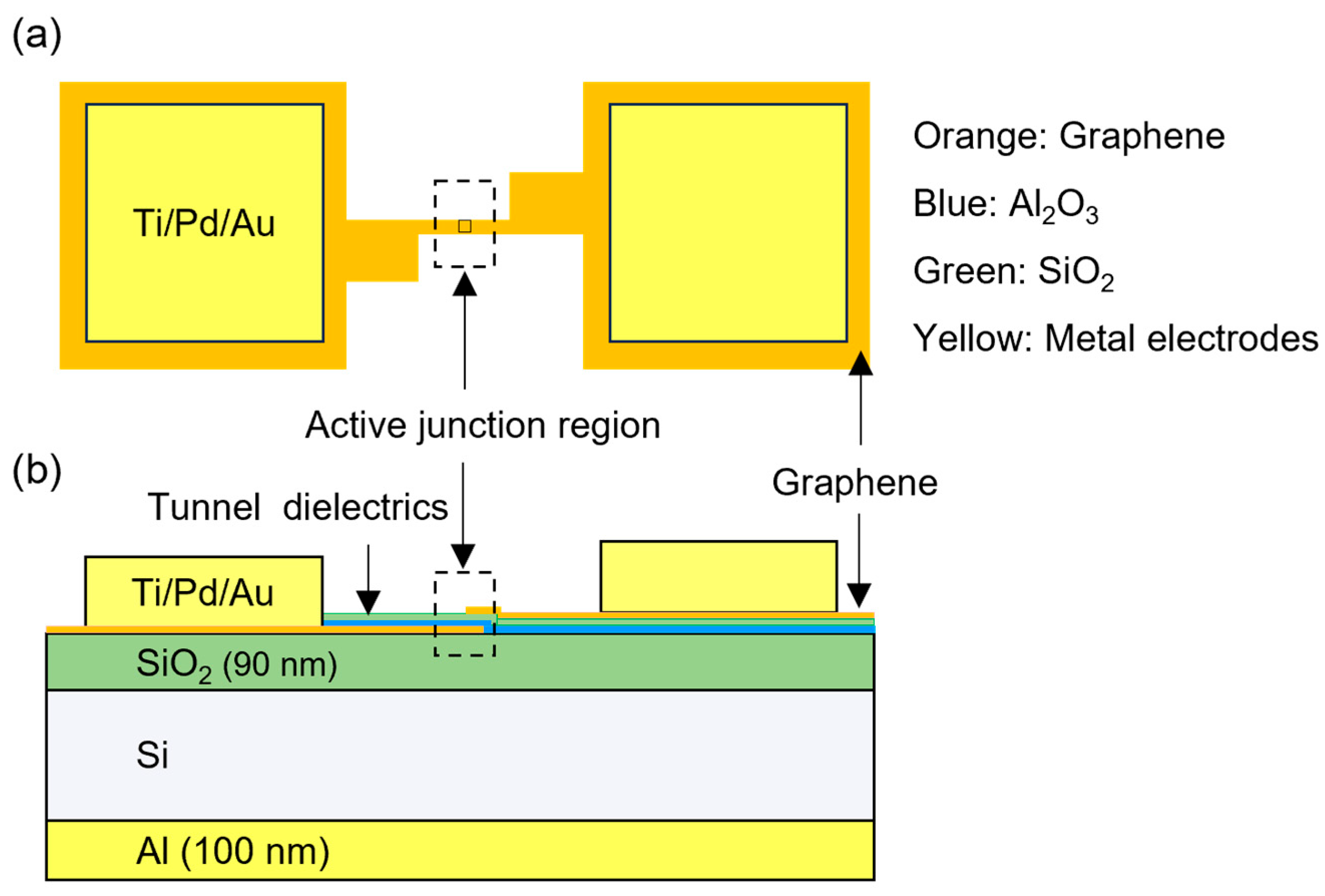
Figure 1 shows the schematics of the top and cross-sectional views of the GI2G tunnel diode. The cross-sectional schematic shows stacked tunnel dielectrics between graphene electrodes. Because the tunneling current depends exponentially on the insulator thickness, the tunnel barrier was formed using atomic layer deposition (ALD), which enables nanometer-scale thickness control. Samples with two different tunnel dielectric structures were prepared to investigate the transport mechanism in the diodes (Table 1). A stacked barrier composed of Al2O3/SiO2 was used to achieve asymmetric IV characteristics. In the GI2G structure, the stacked dielectric barrier introduces step tunneling under positive bias due to differences in the electron affinities and band gaps of the two dielectrics (Figure S1). This band alignment results in a polarity-dependent tunnel barrier, where the effective barrier height and tunneling width depend on the polarity of the applied bias. As a result, step tunneling enhances IV asymmetry even when symmetric graphene electrodes are used.
To evaluate the effect of the tunnel region configuration on the IV characteristics, multiple devices with different tunnel region designs were fabricated using the following process. Monolayer graphene grown by chemical vapor deposition on a Cu foil (Graphenea, San Sebastian, Spain) was transferred onto a Si/SiO2 substrate using a method similar to that reported by Shiga et al. [17]. A polymethyl methacrylate (PMMA) support layer was formed on the top surface of the Cu foil. To remove graphene grown on the back of the Cu foil, a 10% polyvinyl alcohol (PVA) solution was spin-coated on the back surface. The PVA layer, together with the unwanted graphene, was first removed using an iron nitrate solution, after which the Cu foil was etched in the same solution. The remaining graphene/PMMA stack was scooped up with a Si/SiO2 substrate and rinsed twice in pure water. The substrate was left overnight and subsequently annealed in air at 80 °C for 8 h using a drying oven to remove residual water trapped between the graphene and the substrate. Finally, the PMMA layer was removed by immersion in hot acetone. To improve the adhesion at the SiO2/graphene interface, the sample was annealed at 350 °C for 5 h in Ar (500 sccm). A hydrogen silsesquioxane (HSQ) resist was spin-coated, and a fine pattern was defined by electron-beam lithography (JBX-9300SA, JEOL, Tokyo, Japan), followed by patterning of the first graphene layer using O2 reactive ion etching (RIE-10NR, Samco, Kyoto, Japan) at 100 W for 30 s. After patterning, openings in the HSQ layer were defined by photolithography, and the exposed HSQ was removed using buffered oxide etchant (BOE). Ti/Pd/Au (0.5/20/70 nm) layers were deposited by electron-beam evaporation (TU-8, Asahi Shokai Sendai, Sendai, Japan) and lift-off to form electrodes on the graphene. The entire substrate was coated with a 1.5 nm-thick Al layer by electron-beam evaporation and naturally oxidized to form a thin Al2O3 passivation layer. Based on the Pilling–Bedworth relationship [49] and assuming a γ-Al2O3 density of 3.70 g/cm3, the 1.5 nm-thick Al layer formed an Al2O3 layer with an estimated thickness of 2.0 nm [50]. The naturally oxidized Al2O3 layer was used to passivate the graphene surface and to provide a uniform nucleation layer for subsequent ALD. Additional tunnel dielectrics consisting of 3 nm-thick Al2O3 and 3- or 6 nm-thick SiO2 layers were then deposited by ALD (AD-230LP, Samco, Kyoto, Japan). The Al2O3 layer was grown by thermal ALD at 200 °C using trimethylaluminum (TMA) and H2O as the precursor and oxidant, respectively. The SiO2 layer was deposited by plasma-assisted ALD at 200 °C using bis(diethylamino)silane (BDEAS) as the precursor and O2 plasma as the oxidant. ALD enables precise control of dielectric thickness and is widely used in Si processing, providing stable and reproducible interfaces with Si and metal electrodes. A second graphene layer was then transferred onto the tunnel dielectrics. To increase adhesion between graphene and ALD-SiO2, the sample was again annealed at 350 °C for 4 h in Ar (500 sccm). The second graphene layer was coated with HSQ, and a fine pattern was defined by electron-beam lithography followed by O2 reactive-ion etching at 100 W for 30 s. Contact openings were defined by photolithography, and the exposed HSQ within the openings was removed by using BOE. Ti/Pd/Au (0.5/20/70 nm) layers were deposited on the top graphene layer by a separate electron-beam evaporation (ADS-E810, R-DEC, Tsukuba, Japan), and electrodes were formed by lift-off. Because the tunnel dielectrics covered the bottom electrode, additional photolithography and etching steps were required to form contact windows to the bottom graphene layer. Finally, 100 nm-thick Al was deposited on the backside of the Si substrate to form the electrode. We also fabricated metal–double-insulator–Si (MI2S) tunnel diodes with a device area of 5.2 mm2 using the same Al2O3/SiO2 tunnel barrier to evaluate the asymmetry of the IV characteristics. Al electrodes with a thickness of 100 nm were formed on the dielectric layers and on the backside of the Si substrate.

2.2. Electrical and Optical Measurements

The IV characteristics of the fabricated devices were measured using a manual probe station (MPS150, Cascade Microtech, Beaverton, OR, USA) combined with a semiconductor parameter analyzer (4155C, Keysight Technologies, Santa Rosa, CA, USA). The capacitance–voltage (CV) characteristics of the MI2S diodes were measured using a precision LCR meter (4284A, Keysight Technologies) at 1 MHz, with the voltage sweep covering the accumulation and inversion regions. Photocurrent measurements were performed using a standard solar simulator (HAL-320, Asahi Spectra Inc., Tokyo, Japan) providing AM 1.5G illumination, which was positioned to expose the devices uniformly during measurements. The illumination intensity was calibrated to 1-sun conditions over the wavelength range of 350–1100 nm. We evaluated more than 100 devices per sample, and each device was measured multiple times to confirm reproducibility. A field-emission scanning electron microscope (SU8000, Hitachi, Tokyo, Japan) was used to analyze the device structure. Raman measurements were performed using a Raman microscope (InVia, Renishaw, Wotton-under-Edge, UK), and the spectra were recorded with a 50× objective at an excitation wavelength of 532 nm and a laser power of 0.5 mW.

3. Results and Discussion

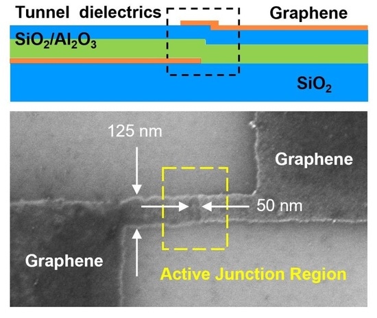
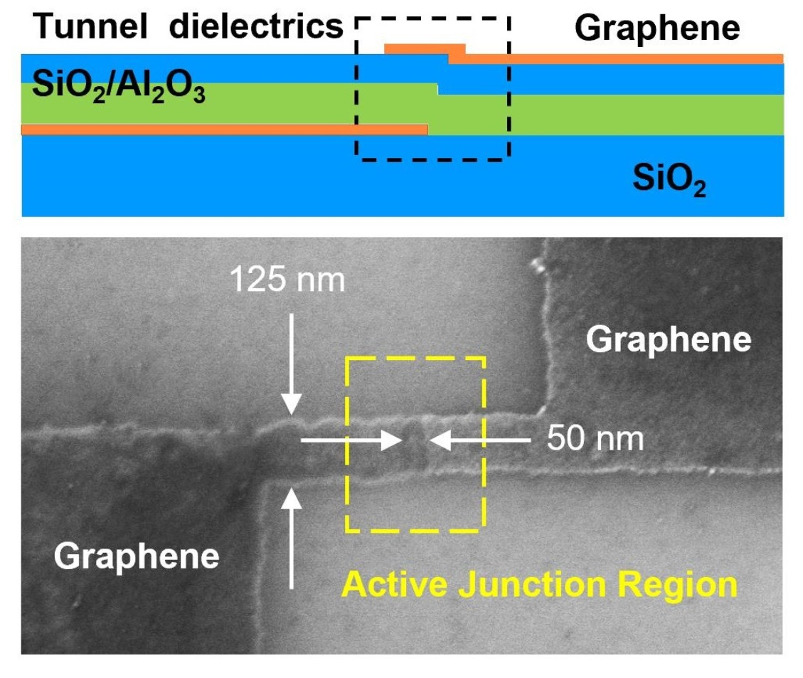
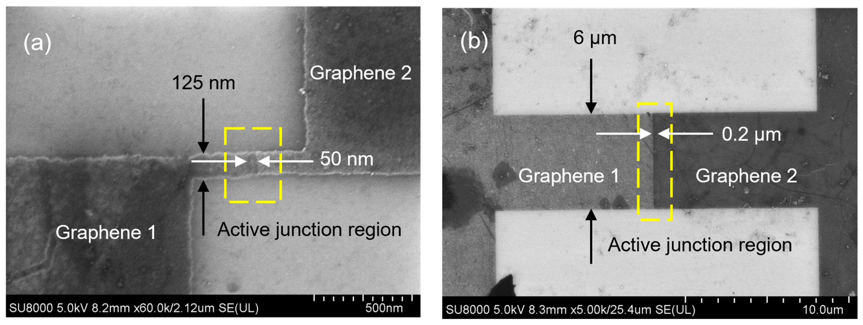
We initially performed Raman measurements on graphene transferred onto thermally oxidized SiO2 substrates. The Raman spectra showed that the transferred graphene was a monolayer with a low defect density (Figure S2). Figure 2 shows field emission scanning electron microscope images of representative GI2G devices. The active junction region, defined by the graphene overlap area, is highlighted by dashed squares. The device shown in Figure 2a has a small antenna with an overlap area of 125 × 50 nm, whereas the device in Figure 2b features a large antenna with an overlap area of 6 × 0.2 µm. Electron-beam lithography enabled precise pattern alignment and the fabrication of features with a minimum dimension of around 50 nm, allowing systematic evaluation of junction geometry and antenna size effects.
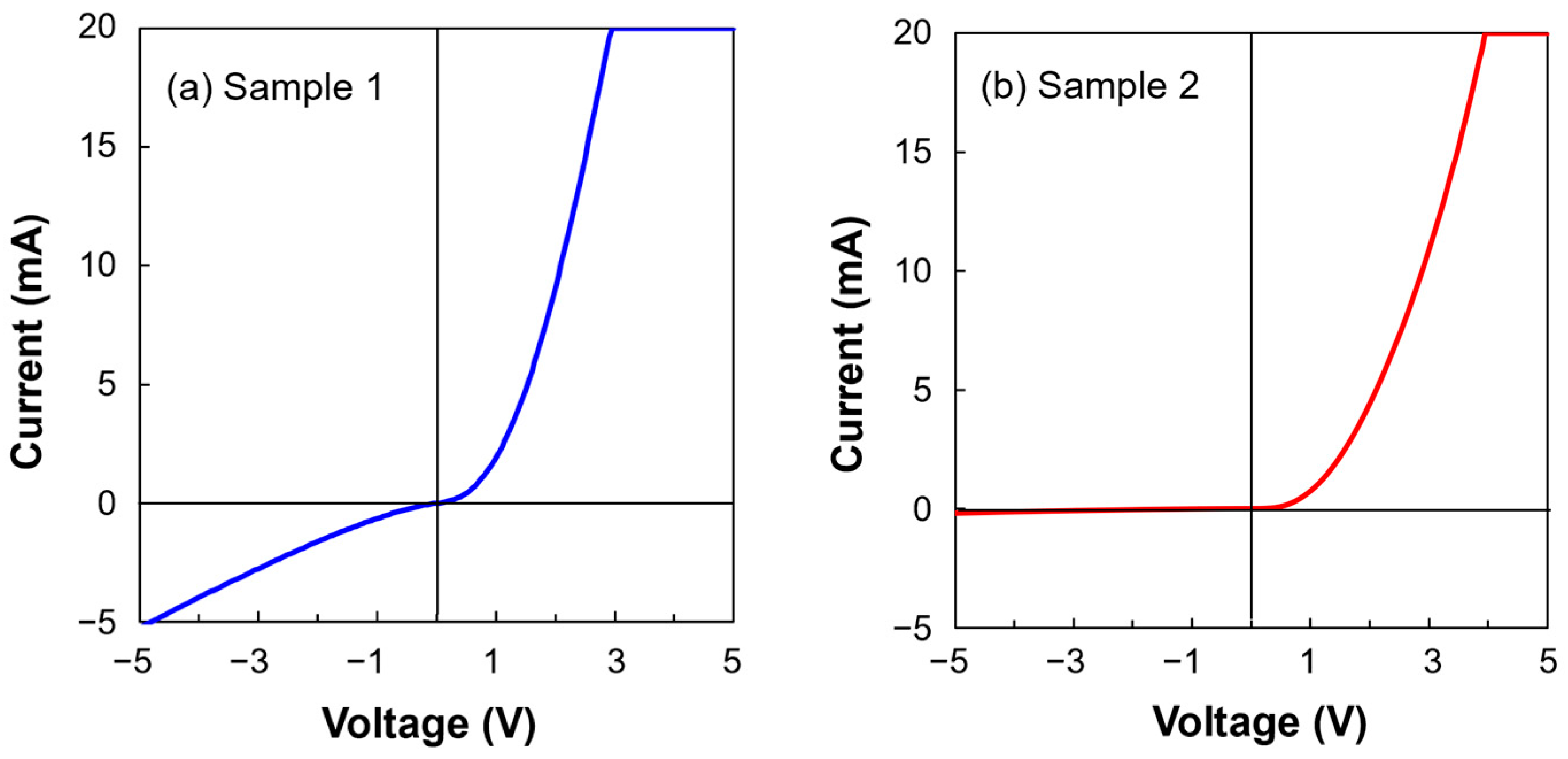
Figure 3 shows representative IV characteristics of the MI2S diodes for the two structures summarized in Table 1. Asymmetric IV characteristics were observed because of the asymmetric tunnel barrier profile of the Al2O3/SiO2 stack, resulting in reduced tunneling current in the reverse-bias region. Sample 1 exhibited a higher current than Sample 2 because of the thinner stacked dielectric layers.
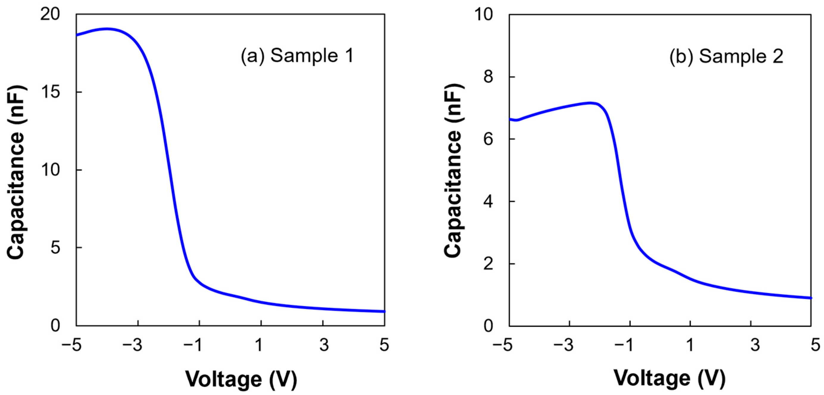
Figure 4 shows representative CV characteristics of the MI2S diodes for the two device structures. The devices exhibited typical p-type substrate behavior, showing an accumulation region under reverse bias and a decrease in capacitance under forward bias. Compared with Sample 1, Sample 2 exhibited lower capacitance because of the thicker SiO2 layer. The relative dielectric constant of the ALD-Al2O3 layer was extracted from the accumulation capacitance at 1 MHz and found to be 9.0, consistent with previously reported values [51].
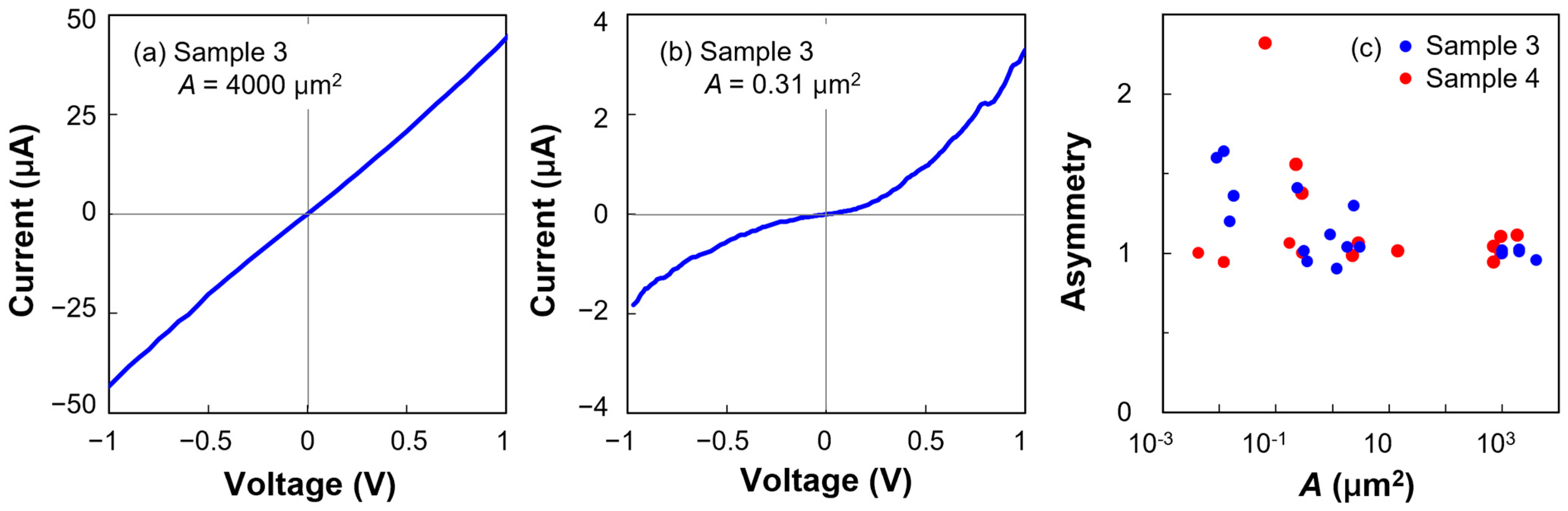
Figure 5 shows IV characteristics and the junction area dependence of the asymmetry. The overall device yield was approximately 52%. The junction areas were defined by electron-beam lithography, which provides high alignment accuracy and ensures good uniformity of the designed junction dimensions. The device-to-device variation is shown in Figure 5c, which summarizes the performance metrics measured across multiple devices.
A large-area device with an active junction area of 4000 µm2 exhibited nearly symmetric IV behavior, whereas a nanoscale device with an active junction area of 0.31 µm2 showed pronounced nonlinearity and asymmetry. The extracted asymmetry, defined as the ratio of current at V of ±1 V, increased systematically with decreasing junction area, as summarized for multiple devices in Figure 5c. Diode characteristics were observed for Samples 3 and 4 when the junction area was sufficiently small, and increased nonlinearity was obtained in devices with miniaturized antenna structures [48]. The nonlinear and asymmetric IV characteristics were mainly associated with the formation of small graphene overlap regions defined by electron-beam lithography. These results suggest that geometric effects can induce IV asymmetry more effectively than stacking dielectric layers with different band gaps and electron affinities. The electric-field concentration and edge-dominated transport in the small overlap region likely amplified the nonlinear IV characteristics of the tunnel junction. Developing a quantitative framework that incorporates geometry-dependent electric fields and transport physics will be important for future analysis.
Although the stacked Al2O3/SiO2 dielectrics formed an asymmetric tunnel barrier, large-area GI2G devices exhibited nearly linear IV characteristics because tunneling current was area-averaged between symmetric graphene electrodes. Owing to their thinner tunnel dielectrics, Sample 3 devices exhibited currents 102–103 times larger than those of Sample 4 devices. In contrast, Sample 4 devices showed greater nonlinearity, which was attributed to the thicker SiO2 layer suppressing the tunneling current.
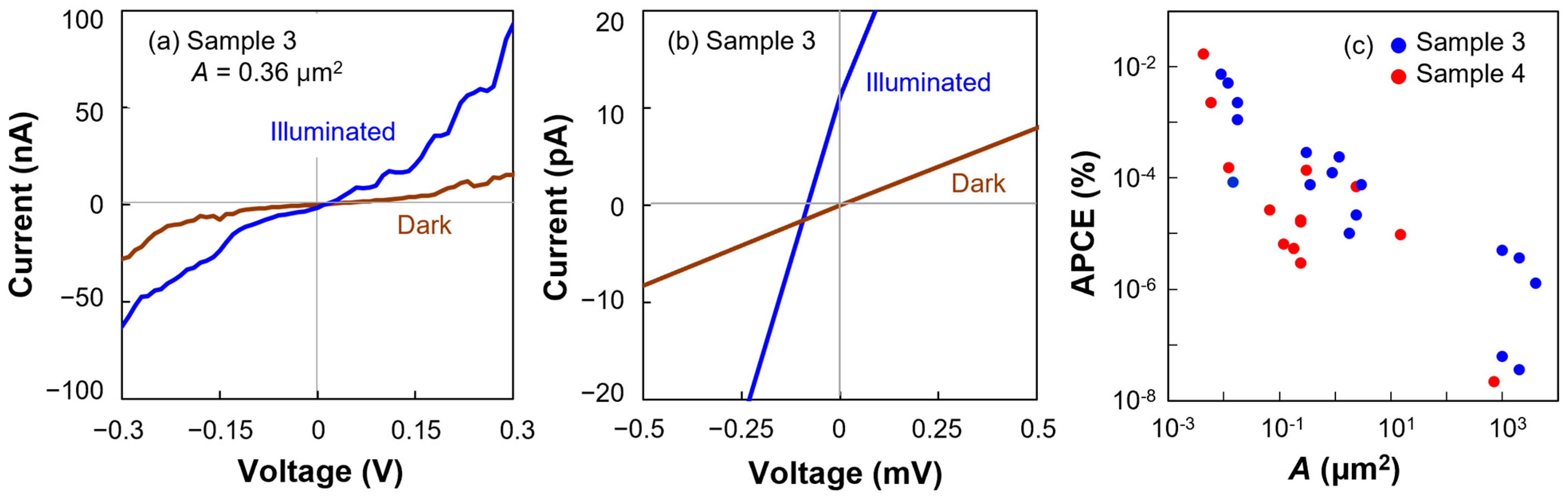
The photoresponse characteristics of Sample 3 devices were evaluated (Figure 6). When the device was illuminated with simulated solar light, an increase in current attributed to the photoconductive effect occurred, indicating the generation of charge carriers in graphene. Photoresponse behavior was observed for Samples 3 and 4 devices. In particular, Sample 3 devices showed a larger modulation current and higher photoresponsivity compared with Sample 4 devices. Furthermore, the photoresponse was measured under zero bias conditions, and a measurable current was observed without an applied bias voltage (Figure 6b). The apparent power conversion efficiency (APCE) increased with decreasing graphene overlap area, reaching approximately 0.01% (Figure 6c). Sample 3 devices exhibited a slightly higher APCE compared with Sample 4 devices, suggesting that asymmetric and nonlinear diode characteristics might play an important role in the observed photoresponse. Although the definitions of efficiency and measurement conditions differ across studies, our result is comparable to graphene geometric diodes [47] and higher than several reported CNT-based diodes [44,45], point-contact MIM diodes [40], and MI2M diodes [43], which typically exhibit efficiencies in the range of 10−3% or less. Reported efficiencies in these devices were often limited by low optical absorption, series resistance, and impedance mismatch between the antenna and diode. The graphene-based tunnel diodes may help mitigate some of these limitations. It should be noted that the APCE represents the apparent device-level power conversion efficiency and may include contributions from both high-frequency rectification and thermal effects arising from illumination. Further wavelength-resolved analysis will be necessary to clarify the underlying mechanism.

4. Conclusions

We fabricated graphene-based vertical tunnel diodes with Al2O3/SiO2 dielectrics of different band gaps and electron affinities, sandwiched between graphene layers. The diodes exhibited asymmetric IV characteristics, with a small overlap region defined by electron-beam lithography. Geometric asymmetry introduced by reducing the graphene overlap area was key to increasing diode nonlinearity, surpassing the effect of the dielectric structure alone.
Photoresponse measurements under AM1.5G illumination revealed a clear photocurrent, suggesting a possible rectification-related response. The photoresponse increased with decreasing junction area, which is consistent with the observed asymmetric behavior. These results suggest that electric-field concentration and edge-dominated transport in nanoscale junctions may improve rectification behavior.
Although the optical absorption efficiency of the device was not quantitatively evaluated in this study, integrating this device into plasmonic nanostructures may increase optical absorption via localized surface plasmon excitation [52]. The present findings highlight the potential of GI2G tunnel diodes for next-generation energy harvesting and optical sensing applications.

Supplementary Materials

The following supporting information can be downloaded at: https://www.mdpi.com/article/10.3390/c12010018/s1. Figure S1: Schematic energy band diagrams of the GI2G structure and Figure S2: Raman spectrum of graphene on a Si/SiO2 substrate.

Author Contributions

Conceptualization, T.U.; methodology, T.U., C.T.; investigation, T.U., Y.H., C.T., H.F., A.S., T.O.; resources, T.U., C.T., H.F., A.S., T.O.; data curation, Y.H., T.U.; writing—original draft, T.U.; writing—review editing, Y.H., C.T.; and funding acquisition, T.U. All authors have read and agreed to the published version of the manuscript.

Funding

This work was supported by JSPS KAKENHI (Grant 22K04201) and JKA (Keirin Grant 2022M-181).

Data Availability Statement

The data that support the findings of this study are available from the corresponding author upon reasonable request.

Acknowledgments

This work was supported by JSPS KAKENHI (Grant No. 22K04201) and JKA (Keirin Grant No. 2022M-181). Part of this work was carried out under the Cooperative Research Project Program of RIEC, Tohoku University, and device fabrication was mainly performed using the facilities and equipment of the Nano-Spin Laboratory, RIEC, Tohoku University, Japan. Another part of this work was supported by the Advanced Research Infrastructure for Materials and Nanotechnology in Japan, funded by MEXT (Proposal No. JPMXP1222TU0103). This work was also partially supported by the Beyond 5G Research and Development Project (Grant No. 05901) and the JST MIRAI program.

Conflicts of Interest

The authors have no conflicts to disclose.

References

  1. Rogdakis, K.; Karakostasa, N.; Kymakis, E. Up-scalable emerging energy conversion technologies enabled by 2D materials: From miniature power harvesters towards grid-connected energy systems. Energy Environ. Sci. 2021, 14, 3352–3392. [Google Scholar] [CrossRef]
  2. Mak, K.F.; Lee, C.; Hone, J.; Shan, J.; Heinz, T.F. Atomically thin MoS2: A new direct-gap semiconductor. Phys. Rev. Lett. 2010, 105, 136805. [Google Scholar] [CrossRef] [PubMed]
  3. Splendiani, A.; Sun, L.; Zhang, Y.; Li, T.; Kim, J.; Chim, C.; Galli, G.; Wang, F. Emerging photoluminescence in monolayer MoS2. Nano Lett. 2010, 10, 1271–1275. [Google Scholar] [CrossRef]
  4. Otsuji, T.; Popov, V.; Ryzhii, V. Active graphene plasmonics for terahertz device applications. J. Phys. D 2014, 47, 094006. [Google Scholar] [CrossRef]
  5. Chernikov, A.; Berkelbach, T.C.; Hill, H.M.; Rigosi, A.; Li, Y.; Aslan, B.; Reichman, D.R.; Hybertsen, M.S.; Heinz, T.F. Exciton binding energy and nonhydrogenic Rydberg series in monolayer WS2. Phys. Rev. Lett. 2014, 113, 076802. [Google Scholar] [CrossRef]
  6. Liu, X.; Galfsky, T.; Sun, Z.; Xia, F.; Lin, E.; Lee, Y.-H.; Kena-Cohen, S.; Menon, V.M. Strong light-matter coupling in two-dimensional atomic crystals. Nat. Photonics 2015, 9, 30–34. [Google Scholar] [CrossRef]
  7. Rivera, P.; Schaibley, J.R.; Jones, A.M.; Ross, J.S.; Wu, S.; Aivazian, G.; Klement, P.; Seyler, K.; Clark, G.; Ghimire, N.J.; et al. Observation of long-lived interlayer excitons in monolayer MoSe2-WSe2 heterostructures. Nat. Commun. 2015, 6, 6242. [Google Scholar] [CrossRef] [PubMed]
  8. Hendry, E.; Hale, P.J.; Moger, J.; Savchenko, A.K.; Bonn, M. Coherent nonlinear optical response of graphene. Phys. Rev. Lett. 2010, 105, 097401. [Google Scholar] [CrossRef]
  9. Soavi, G.; Wang, G.; Rostami, H.; Purdie, D.G.; De Fazio, D.; Ma, T.; Luo, B.; Wang, J.; Ott, A.K.; Yoon, D.; et al. Broadband, electrically tunable third-harmonic generation in graphene. Nat. Nanotechnol. 2018, 13, 583–588. [Google Scholar] [CrossRef]
  10. Novoselov, K.S.; Geim, A.K.; Morozov, S.V.; Jiang, D.; Katsnelson, M.I.; Grigorieva, I.V.; Dubonos, S.V.; Firsov, A.A. Two-dimensional gas of massless Dirac fermions in graphene. Nature 2005, 438, 197–200. [Google Scholar] [CrossRef] [PubMed]
  11. Dean, C.R.; Young, A.F.; Meric, I.; Lee, C.; Wang, L.; Sorgenfrei, S.; Watanabe, K.; Taniguchi, T.; Kim, P.; Shepard, K.L.; et al. Boron nitride substrates for high-quality graphene electronics. Nat. Nanotechnol. 2010, 5, 722–726. [Google Scholar] [CrossRef]
  12. Cui, C.; Xue, F.; Hu, W.-J.; Lee, J. Two-dimensional materials with piezoelectric and ferroelectric properties. npj 2D Mater. Appl. 2018, 2, 18. [Google Scholar] [CrossRef]
  13. Zhang, Y.; Tang, T.-T.; Girit, C.; Hao, Z.; Martin, M.C.; Zettl, A.; Crommie, M.F.; Shen, Y.R.; Wang, F. Direct observation of a widely tunable bandgap in bilayer graphene. Nature 2009, 459, 820–823. [Google Scholar] [CrossRef]
  14. Chaves, A.; Azadani, J.G.; Alsalman, H.; da Costa, D.R.; Frisenda, R.; Chaves, A.J.; Song, S.H.; Kim, Y.D.; He, D.; Singh, R. Bandgap engineering of two-dimensional semiconductor materials. npj 2D Mater. Appl. 2020, 4, 29. [Google Scholar] [CrossRef]
  15. Uchino, T.; Ayre, G.; Smith, D.C.; Hutchison, J.L.; de Groot, C.H.; Ashburn, P. The effects of hydrogen annealing on carbon nanotube field-effect transistors. Nanomaterials 2021, 11, 2481. [Google Scholar] [CrossRef]
  16. Chen, X.; Shehzad, K.; Gao, L.; Long, M.; Guo, H.; Qin, S.; Wang, X.; Wang, F.; Shi, Y.; Hu, W.; et al. Graphene hybrid structures for integrated and flexible optoelectronics. Adv. Mater. 2019, 32, 1902039. [Google Scholar] [CrossRef]
  17. Shiga, K.; Komiyama, T.; Fuse, Y.; Fukidome, H.; Sato, A.; Otsuji, T.; Uchino, T. Electrical transport properties of gate tunable graphene lateral tunnel diodes. Jpn. J. Appl. Phys. 2020, 59, SIID03. [Google Scholar] [CrossRef]
  18. Hemmetter, A.; Yang, X.; Wang, Z.; Otto, M.; Uzlu, B.; Andree, M.; Pfeiffer, U.; Vorobiev, A.; Stake, J.; Lemme, M.C.; et al. Terahertz rectennas on flexible substrates based on one-dimensional metal-insulator-graphene diodes. ACS Appl. Electron. Mat. 2021, 3, 3747–3753. [Google Scholar] [CrossRef]
  19. Geim, A.K.; Novoselov, K.S. The rise of graphene. Nat. Mater. 2007, 6, 183–191. [Google Scholar] [CrossRef]
  20. Bonaccorso, F.; Sun, Z.; Hasan, T.; Ferrari, A.C. Graphene photonics and optoelectronics. Nat. Photon. 2010, 4, 611–622. [Google Scholar] [CrossRef]
  21. Schedin, F.; Geim, A.K.; Morozov, S.V.; Hill, E.W.; Blake, P.; Katsnelson, M.I.; Novoselov, K.S. Detection of individual gas molecules adsorbed on graphene. Nat. Mater. 2007, 6, 652–655. [Google Scholar] [CrossRef]
  22. Xie, J.; Chen, Q.; Shen, H.; Li, G. Review-wearable graphene devices for sensing. J. Electrochem. Soc. 2020, 167, 037541. [Google Scholar] [CrossRef]
  23. Uchino, T.; Heng, Y.; Tang, C.; Kasai, S.; Fukidome, H.; Sato, A.; Ikeda, S.; Otsuji, T. Improved sensitivity in graphene-mediated surface-enhanced Raman scattering via H2/Ar annealing. J. Appl. Phys. 2025, 138, 174503. [Google Scholar] [CrossRef]
  24. Liu, M.; Yang, L.; Cao, C.; Cao, X.; Cheng, Y.; Luo, H.; Chen, F.; Li, X. Switchable narrowband/broadband terahertz metasurface absorber based on single-layer graphene structure. Diam. Relat. Mater. 2026, 161, 113199. [Google Scholar] [CrossRef]
  25. Robinson, J.A.; Hollander, M.; LaBella, M.; Trumbull, K.A.; Cavalero, R.; Snyder, D.W. Contacting graphene. Appl. Phys. Lett. 2011, 98, 053103. [Google Scholar] [CrossRef]
  26. Farmer, D.B.; Lin, Y.M.; Afzali, A.; Avouris, P. Behavior of a chemically doped graphene junction. Appl. Phys. Lett. 2009, 94, 213106. [Google Scholar] [CrossRef]
  27. Li, S.; Mi, H.; Li, M.; Wang, J.; Su, N. Enhancing the uniformity and stability of graphene-based devices via Si3N4 film-assisted patterning. Mat. Sci. Semicon. Proc. 2025, 195, 109618. [Google Scholar] [CrossRef]
  28. Brown, W.C. Space Oriented Microwave Power Transmission System. U.S. Patent 3,434,678, 25 March 1969. [Google Scholar]
  29. Brown, W.C. The history of power transmission by radio waves. IEEE Trans. Microw. Theory Tech. 1984, 32, 1230–1242. [Google Scholar] [CrossRef]
  30. Bailey, R.L. A proposed new concept for a solar-energy converter. J. Eng. Power 1972, 94, 73–77. [Google Scholar] [CrossRef]
  31. Corkish, R.; Green, M.; Puzzer, T. Solar energy collection by antennas. Sol. Energy 2002, 73, 395–401. [Google Scholar] [CrossRef]
  32. Donchev, E.; Pang, J.S.; Gammon, P.M.; Centeno, A.; Xie, F.; Petrov, P.K.; Breeze, J.D.; Ryan, M.P.; Riley, D.J.; Alford, N.M. The rectenna device: From theory to practice (a review). MRS Energy Sustain. 2014, 1, E1. [Google Scholar] [CrossRef]
  33. Shanawani, M.; Masotti, D.; Costanzo, A. THz rectennas and their design rules. Electronics 2017, 6, 99. [Google Scholar] [CrossRef]
  34. McSpadden, J.O.; Yoo, T.; Chang, K. Theoretical and experimental investigation of a rectenna element for microwave power transmission. IEEE Trans. Microw. Theory Tech. 1992, 40, 2359–2366. [Google Scholar] [CrossRef]
  35. Wang, X.; Fan, F. Design of a 35 GHz circularly polarized rectenna for wireless power transmission. In Proceedings of the 2019 International Symposium on Antennas and Propagation (ISAP, 2019), Xi’an, China, 27–30 October 2019; pp. 558–560. [Google Scholar]
  36. Hagerty, J.A.; Helmbrecht, F.B.; McCalpin, W.H.; Zane, R.; Popovic, Z.B. Recycling ambient microwave energy with broad-band rectenna arrays. IEEE Trans. Microw. Theory Tech. 2004, 52, 1014–1024. [Google Scholar] [CrossRef]
  37. Gadalla, M.N.; Abdel-Rahman, M.; Shamim, A. Design, optimization and fabrication of a 28.3 THz nano-rectenna for infrared detection and rectification. Sci. Rep. 2014, 4, 4270. [Google Scholar] [CrossRef]
  38. Jayaswal, G.; Belkadi, A.; Meredov, A.; Pelz, B.; Moddel, D.; Shamim, A. Optical rectification through an Al2O3 based MIM passive rectenna at 28.3 THz. Mater. Today Energy 2018, 7, 1–9. [Google Scholar] [CrossRef]
  39. Tekin, S.B.; Almalki, S.; Finch, H.; Vezzoli, A.; O’Brien, L.; Dhanak, V.R.; Hall, S.; Mitrovic, I.Z. Electron affinity of metal oxide thin films of TiO2, ZnO, and NiO and their applicability in 28.3 THz rectenna devices. J. Appl. Phys. 2023, 134, 084503. [Google Scholar] [CrossRef]
  40. Mupparapu, R.; Cunha, J.; Tantussi, F.; Jacassi, A.; Summerer, L.; Patrini, M.; Giugni, A.; Maserati, L.; Alabastri, A.; Garoli, D.; et al. High-frequency light rectification by nanoscale plasmonic conical antenna in point-contact-insulator-metal architecture. Adv. Energy Mat. 2022, 12, 2103785. [Google Scholar] [CrossRef]
  41. Citroni, R.; Di Paolo, F.; Livreri, P. Progress in THz rectifier technology: Research and perspectives. Nanomaterials 2022, 12, 2479. [Google Scholar] [CrossRef] [PubMed]
  42. Berland, B. Photovoltaic Technologies Beyond the Horizon: Optical Rectenna Solar Cell, Final Report; NREL/SR-520-33263; National Renewable Energy Lab. NREL: Golden, CO, USA, 2003. [Google Scholar]
  43. Belkadi, A.; Weerakkody, A.; Moddel, G. Demonstration of resonant tunneling effects in metal-double-insulator-metal (MI2M) diodes. Nat. Commun. 2021, 12, 2925. [Google Scholar] [CrossRef] [PubMed]
  44. Sharma, A.; Singh, V.; Bougher, T.L.; Cola, B.A. A carbon nanotube optical rectenna. Nat. Nanotech. 2015, 10, 1027–1032. [Google Scholar] [CrossRef]
  45. Anderson, E.C.; Bougher, T.L.; Cola, B.A. Optical rectennae: High performance multiwall carbon nanotube-insulator-metal tunnel diode arrays for optical rectification. Adv. Electron. Mater. 2018, 4, 1870017. [Google Scholar] [CrossRef]
  46. Tizani, L.; Abbas, Y.; Yassin, A.M.; Mohammad, B.; Rezeq, M. Single wall carbon nanotube based optical rectenna. RSC Adv. 2021, 11, 24116. [Google Scholar] [CrossRef]
  47. Zhu, Z.; Joshi, S.; Grover, S.; Moddel, G. Graphene geometric diodes for terahertz rectennas. J. Phys. D Appl. Phys. 2013, 46, 185101. [Google Scholar] [CrossRef]
  48. Shin, J.H.; Yang, J.H.; Heo, S.J.; Jang, J.E. Geometric effect in a vertical stack-up metal-insulator-metal tunnel diode. AIP Adv. 2017, 7, 105307. [Google Scholar] [CrossRef]
  49. Pilling, N.; Bedworth, R.J. The oxidation of metals at high temperatures. J. Inst. Met. 1923, 29, 529. [Google Scholar]
  50. Lide, D.R. CRC Handbook of Chemistry and Physics, 84th ed.; CRC Press: New York, NY, USA, 2003; pp. 4–38. [Google Scholar]
  51. Wilk, G.D.; Wallace, R.M.; Anthony, J.M. High-κ gate dielectrics: Current status and materials properties considerations. J. Appl. Phys. 2001, 89, 5243–5275. [Google Scholar] [CrossRef]
  52. Echtermeyer, T.J.; Britnell, L.; Jasnos, P.K.; Lombardo, A.; Gorbachev, R.V.; Grigorenko, A.N.; Geim, A.K.; Ferrari, A.C.; Novoselov, K.S. Strong plasmonic enhancement of photovoltage in graphene. Nat. Commun. 2011, 2, 458. [Google Scholar] [CrossRef] [PubMed]
Figure 1. Schematic illustration of the GI2G device. (a) Top view of the device (not to scale). (b) Corresponding cross-sectional structure (not to scale). The dashed region indicates the active junction area, where the graphene electrodes are separated by tunnel dielectric layers.
Carbon 12 00018 g001
Figure 2. SEM images of GI2G devices. The active junction region is highlighted by dashed squares. (a) Device with a small antenna and an overlap area of 125 × 50 nm. (b) Device with a large antenna and an overlap area of 6 × 0.2 µm.
Carbon 12 00018 g002
Figure 3. Comparison of the IV characteristics of Samples (a) 1 and (b) 2 with an area of 5.2 mm2, demonstrating different nonlinear behavior related to the dielectric structures.
Carbon 12 00018 g003
Figure 4. CV characteristics of the MI2S diodes with an area of 5.2 mm2 for Samples (a) 1 and (b) 2.
Carbon 12 00018 g004
Figure 5. IV characteristics of Sample 3 with different junction areas (A) of (a) 4000 and (b) 0.31 µm2. (c) Dependence of the extracted asymmetry on A, showing increased asymmetry for smaller devices (Samples 3 and 4).
Carbon 12 00018 g005
Figure 6. (a) IV characteristics of Sample 3 with a junction area (A) of 0.36 μm2, measured in the dark (brown) and under illumination (blue). (b) Photoresponse characteristics of Sample 3 under dark and illuminated conditions near zero bias. (c) Dependence of the apparent power conversion efficiency (APCE) on A (Samples 3 and 4).
Carbon 12 00018 g006
Table 1. Structural parameters of the fabricated samples.
SampleDevice StructureDielectrics I1/I2
Sample 1p-Si/I1/I2/AlAl2O3 (3 nm)/SiO2 (3 nm)
Sample 2p-Si/I1/I2/AlAl2O3 (3 nm)/SiO2 (6 nm)
Sample 3Graphene/I1/I2/GrapheneAl2O3 (2 + 3 nm)/SiO2 (3 nm)
Sample 4Graphene/I1/I2/GrapheneAl2O3 (2 + 3 nm)/SiO2 (6 nm)
Disclaimer/Publisher’s Note: The statements, opinions and data contained in all publications are solely those of the individual author(s) and contributor(s) and not of MDPI and/or the editor(s). MDPI and/or the editor(s) disclaim responsibility for any injury to people or property resulting from any ideas, methods, instructions or products referred to in the content.