
Rectifying and Photoconductive Responses in Graphene–Double-Insulator–Graphene (GI2G) Structures

 , , ,
, , ,
Abstract
1. Introduction
2. Materials and Methods
2.1. Device Fabrication
2.2. Electrical and Optical Measurements
3. Results and Discussion
4. Conclusions
Supplementary Materials
Author Contributions
Funding
Data Availability Statement
Acknowledgments
Conflicts of Interest
References
- Rogdakis, K.; Karakostasa, N.; Kymakis, E. Up-scalable emerging energy conversion technologies enabled by 2D materials: From miniature power harvesters towards grid-connected energy systems. Energy Environ. Sci. 2021, 14, 3352–3392. [Google Scholar] [CrossRef]
- Mak, K.F.; Lee, C.; Hone, J.; Shan, J.; Heinz, T.F. Atomically thin MoS2: A new direct-gap semiconductor. Phys. Rev. Lett. 2010, 105, 136805. [Google Scholar] [CrossRef] [PubMed]
- Splendiani, A.; Sun, L.; Zhang, Y.; Li, T.; Kim, J.; Chim, C.; Galli, G.; Wang, F. Emerging photoluminescence in monolayer MoS2. Nano Lett. 2010, 10, 1271–1275. [Google Scholar] [CrossRef]
- Otsuji, T.; Popov, V.; Ryzhii, V. Active graphene plasmonics for terahertz device applications. J. Phys. D 2014, 47, 094006. [Google Scholar] [CrossRef]
- Chernikov, A.; Berkelbach, T.C.; Hill, H.M.; Rigosi, A.; Li, Y.; Aslan, B.; Reichman, D.R.; Hybertsen, M.S.; Heinz, T.F. Exciton binding energy and nonhydrogenic Rydberg series in monolayer WS2. Phys. Rev. Lett. 2014, 113, 076802. [Google Scholar] [CrossRef]
- Liu, X.; Galfsky, T.; Sun, Z.; Xia, F.; Lin, E.; Lee, Y.-H.; Kena-Cohen, S.; Menon, V.M. Strong light-matter coupling in two-dimensional atomic crystals. Nat. Photonics 2015, 9, 30–34. [Google Scholar] [CrossRef]
- Rivera, P.; Schaibley, J.R.; Jones, A.M.; Ross, J.S.; Wu, S.; Aivazian, G.; Klement, P.; Seyler, K.; Clark, G.; Ghimire, N.J.; et al. Observation of long-lived interlayer excitons in monolayer MoSe2-WSe2 heterostructures. Nat. Commun. 2015, 6, 6242. [Google Scholar] [CrossRef] [PubMed]
- Hendry, E.; Hale, P.J.; Moger, J.; Savchenko, A.K.; Bonn, M. Coherent nonlinear optical response of graphene. Phys. Rev. Lett. 2010, 105, 097401. [Google Scholar] [CrossRef]
- Soavi, G.; Wang, G.; Rostami, H.; Purdie, D.G.; De Fazio, D.; Ma, T.; Luo, B.; Wang, J.; Ott, A.K.; Yoon, D.; et al. Broadband, electrically tunable third-harmonic generation in graphene. Nat. Nanotechnol. 2018, 13, 583–588. [Google Scholar] [CrossRef]
- Novoselov, K.S.; Geim, A.K.; Morozov, S.V.; Jiang, D.; Katsnelson, M.I.; Grigorieva, I.V.; Dubonos, S.V.; Firsov, A.A. Two-dimensional gas of massless Dirac fermions in graphene. Nature 2005, 438, 197–200. [Google Scholar] [CrossRef] [PubMed]
- Dean, C.R.; Young, A.F.; Meric, I.; Lee, C.; Wang, L.; Sorgenfrei, S.; Watanabe, K.; Taniguchi, T.; Kim, P.; Shepard, K.L.; et al. Boron nitride substrates for high-quality graphene electronics. Nat. Nanotechnol. 2010, 5, 722–726. [Google Scholar] [CrossRef]
- Cui, C.; Xue, F.; Hu, W.-J.; Lee, J. Two-dimensional materials with piezoelectric and ferroelectric properties. npj 2D Mater. Appl. 2018, 2, 18. [Google Scholar] [CrossRef]
- Zhang, Y.; Tang, T.-T.; Girit, C.; Hao, Z.; Martin, M.C.; Zettl, A.; Crommie, M.F.; Shen, Y.R.; Wang, F. Direct observation of a widely tunable bandgap in bilayer graphene. Nature 2009, 459, 820–823. [Google Scholar] [CrossRef]
- Chaves, A.; Azadani, J.G.; Alsalman, H.; da Costa, D.R.; Frisenda, R.; Chaves, A.J.; Song, S.H.; Kim, Y.D.; He, D.; Singh, R. Bandgap engineering of two-dimensional semiconductor materials. npj 2D Mater. Appl. 2020, 4, 29. [Google Scholar] [CrossRef]
- Uchino, T.; Ayre, G.; Smith, D.C.; Hutchison, J.L.; de Groot, C.H.; Ashburn, P. The effects of hydrogen annealing on carbon nanotube field-effect transistors. Nanomaterials 2021, 11, 2481. [Google Scholar] [CrossRef]
- Chen, X.; Shehzad, K.; Gao, L.; Long, M.; Guo, H.; Qin, S.; Wang, X.; Wang, F.; Shi, Y.; Hu, W.; et al. Graphene hybrid structures for integrated and flexible optoelectronics. Adv. Mater. 2019, 32, 1902039. [Google Scholar] [CrossRef]
- Shiga, K.; Komiyama, T.; Fuse, Y.; Fukidome, H.; Sato, A.; Otsuji, T.; Uchino, T. Electrical transport properties of gate tunable graphene lateral tunnel diodes. Jpn. J. Appl. Phys. 2020, 59, SIID03. [Google Scholar] [CrossRef]
- Hemmetter, A.; Yang, X.; Wang, Z.; Otto, M.; Uzlu, B.; Andree, M.; Pfeiffer, U.; Vorobiev, A.; Stake, J.; Lemme, M.C.; et al. Terahertz rectennas on flexible substrates based on one-dimensional metal-insulator-graphene diodes. ACS Appl. Electron. Mat. 2021, 3, 3747–3753. [Google Scholar] [CrossRef]
- Geim, A.K.; Novoselov, K.S. The rise of graphene. Nat. Mater. 2007, 6, 183–191. [Google Scholar] [CrossRef]
- Bonaccorso, F.; Sun, Z.; Hasan, T.; Ferrari, A.C. Graphene photonics and optoelectronics. Nat. Photon. 2010, 4, 611–622. [Google Scholar] [CrossRef]
- Schedin, F.; Geim, A.K.; Morozov, S.V.; Hill, E.W.; Blake, P.; Katsnelson, M.I.; Novoselov, K.S. Detection of individual gas molecules adsorbed on graphene. Nat. Mater. 2007, 6, 652–655. [Google Scholar] [CrossRef]
- Xie, J.; Chen, Q.; Shen, H.; Li, G. Review-wearable graphene devices for sensing. J. Electrochem. Soc. 2020, 167, 037541. [Google Scholar] [CrossRef]
- Uchino, T.; Heng, Y.; Tang, C.; Kasai, S.; Fukidome, H.; Sato, A.; Ikeda, S.; Otsuji, T. Improved sensitivity in graphene-mediated surface-enhanced Raman scattering via H2/Ar annealing. J. Appl. Phys. 2025, 138, 174503. [Google Scholar] [CrossRef]
- Liu, M.; Yang, L.; Cao, C.; Cao, X.; Cheng, Y.; Luo, H.; Chen, F.; Li, X. Switchable narrowband/broadband terahertz metasurface absorber based on single-layer graphene structure. Diam. Relat. Mater. 2026, 161, 113199. [Google Scholar] [CrossRef]
- Robinson, J.A.; Hollander, M.; LaBella, M.; Trumbull, K.A.; Cavalero, R.; Snyder, D.W. Contacting graphene. Appl. Phys. Lett. 2011, 98, 053103. [Google Scholar] [CrossRef]
- Farmer, D.B.; Lin, Y.M.; Afzali, A.; Avouris, P. Behavior of a chemically doped graphene junction. Appl. Phys. Lett. 2009, 94, 213106. [Google Scholar] [CrossRef]
- Li, S.; Mi, H.; Li, M.; Wang, J.; Su, N. Enhancing the uniformity and stability of graphene-based devices via Si3N4 film-assisted patterning. Mat. Sci. Semicon. Proc. 2025, 195, 109618. [Google Scholar] [CrossRef]
- Brown, W.C. Space Oriented Microwave Power Transmission System. U.S. Patent 3,434,678, 25 March 1969. [Google Scholar]
- Brown, W.C. The history of power transmission by radio waves. IEEE Trans. Microw. Theory Tech. 1984, 32, 1230–1242. [Google Scholar] [CrossRef]
- Bailey, R.L. A proposed new concept for a solar-energy converter. J. Eng. Power 1972, 94, 73–77. [Google Scholar] [CrossRef]
- Corkish, R.; Green, M.; Puzzer, T. Solar energy collection by antennas. Sol. Energy 2002, 73, 395–401. [Google Scholar] [CrossRef]
- Donchev, E.; Pang, J.S.; Gammon, P.M.; Centeno, A.; Xie, F.; Petrov, P.K.; Breeze, J.D.; Ryan, M.P.; Riley, D.J.; Alford, N.M. The rectenna device: From theory to practice (a review). MRS Energy Sustain. 2014, 1, E1. [Google Scholar] [CrossRef]
- Shanawani, M.; Masotti, D.; Costanzo, A. THz rectennas and their design rules. Electronics 2017, 6, 99. [Google Scholar] [CrossRef]
- McSpadden, J.O.; Yoo, T.; Chang, K. Theoretical and experimental investigation of a rectenna element for microwave power transmission. IEEE Trans. Microw. Theory Tech. 1992, 40, 2359–2366. [Google Scholar] [CrossRef]
- Wang, X.; Fan, F. Design of a 35 GHz circularly polarized rectenna for wireless power transmission. In Proceedings of the 2019 International Symposium on Antennas and Propagation (ISAP, 2019), Xi’an, China, 27–30 October 2019; pp. 558–560. [Google Scholar]
- Hagerty, J.A.; Helmbrecht, F.B.; McCalpin, W.H.; Zane, R.; Popovic, Z.B. Recycling ambient microwave energy with broad-band rectenna arrays. IEEE Trans. Microw. Theory Tech. 2004, 52, 1014–1024. [Google Scholar] [CrossRef]
- Gadalla, M.N.; Abdel-Rahman, M.; Shamim, A. Design, optimization and fabrication of a 28.3 THz nano-rectenna for infrared detection and rectification. Sci. Rep. 2014, 4, 4270. [Google Scholar] [CrossRef]
- Jayaswal, G.; Belkadi, A.; Meredov, A.; Pelz, B.; Moddel, D.; Shamim, A. Optical rectification through an Al2O3 based MIM passive rectenna at 28.3 THz. Mater. Today Energy 2018, 7, 1–9. [Google Scholar] [CrossRef]
- Tekin, S.B.; Almalki, S.; Finch, H.; Vezzoli, A.; O’Brien, L.; Dhanak, V.R.; Hall, S.; Mitrovic, I.Z. Electron affinity of metal oxide thin films of TiO2, ZnO, and NiO and their applicability in 28.3 THz rectenna devices. J. Appl. Phys. 2023, 134, 084503. [Google Scholar] [CrossRef]
- Mupparapu, R.; Cunha, J.; Tantussi, F.; Jacassi, A.; Summerer, L.; Patrini, M.; Giugni, A.; Maserati, L.; Alabastri, A.; Garoli, D.; et al. High-frequency light rectification by nanoscale plasmonic conical antenna in point-contact-insulator-metal architecture. Adv. Energy Mat. 2022, 12, 2103785. [Google Scholar] [CrossRef]
- Citroni, R.; Di Paolo, F.; Livreri, P. Progress in THz rectifier technology: Research and perspectives. Nanomaterials 2022, 12, 2479. [Google Scholar] [CrossRef] [PubMed]
- Berland, B. Photovoltaic Technologies Beyond the Horizon: Optical Rectenna Solar Cell, Final Report; NREL/SR-520-33263; National Renewable Energy Lab. NREL: Golden, CO, USA, 2003. [Google Scholar]
- Belkadi, A.; Weerakkody, A.; Moddel, G. Demonstration of resonant tunneling effects in metal-double-insulator-metal (MI2M) diodes. Nat. Commun. 2021, 12, 2925. [Google Scholar] [CrossRef] [PubMed]
- Sharma, A.; Singh, V.; Bougher, T.L.; Cola, B.A. A carbon nanotube optical rectenna. Nat. Nanotech. 2015, 10, 1027–1032. [Google Scholar] [CrossRef]
- Anderson, E.C.; Bougher, T.L.; Cola, B.A. Optical rectennae: High performance multiwall carbon nanotube-insulator-metal tunnel diode arrays for optical rectification. Adv. Electron. Mater. 2018, 4, 1870017. [Google Scholar] [CrossRef]
- Tizani, L.; Abbas, Y.; Yassin, A.M.; Mohammad, B.; Rezeq, M. Single wall carbon nanotube based optical rectenna. RSC Adv. 2021, 11, 24116. [Google Scholar] [CrossRef]
- Zhu, Z.; Joshi, S.; Grover, S.; Moddel, G. Graphene geometric diodes for terahertz rectennas. J. Phys. D Appl. Phys. 2013, 46, 185101. [Google Scholar] [CrossRef]
- Shin, J.H.; Yang, J.H.; Heo, S.J.; Jang, J.E. Geometric effect in a vertical stack-up metal-insulator-metal tunnel diode. AIP Adv. 2017, 7, 105307. [Google Scholar] [CrossRef]
- Pilling, N.; Bedworth, R.J. The oxidation of metals at high temperatures. J. Inst. Met. 1923, 29, 529. [Google Scholar]
- Lide, D.R. CRC Handbook of Chemistry and Physics, 84th ed.; CRC Press: New York, NY, USA, 2003; pp. 4–38. [Google Scholar]
- Wilk, G.D.; Wallace, R.M.; Anthony, J.M. High-κ gate dielectrics: Current status and materials properties considerations. J. Appl. Phys. 2001, 89, 5243–5275. [Google Scholar] [CrossRef]
- Echtermeyer, T.J.; Britnell, L.; Jasnos, P.K.; Lombardo, A.; Gorbachev, R.V.; Grigorenko, A.N.; Geim, A.K.; Ferrari, A.C.; Novoselov, K.S. Strong plasmonic enhancement of photovoltage in graphene. Nat. Commun. 2011, 2, 458. [Google Scholar] [CrossRef] [PubMed]



| Sample | Device Structure | Dielectrics I1/I2 |
|---|---|---|
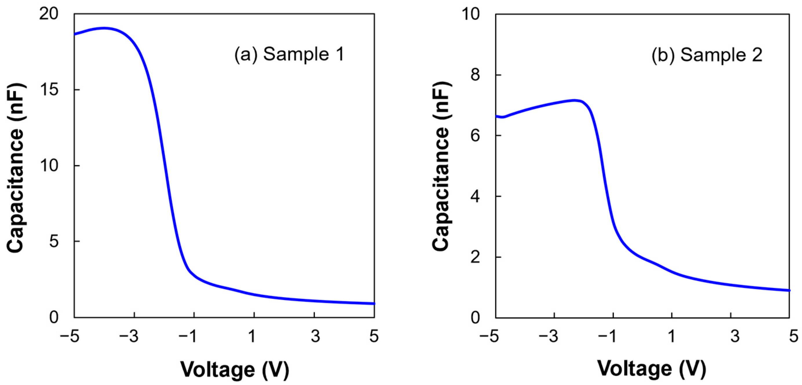
| Sample 1 | p-Si/I1/I2/Al | Al2O3 (3 nm)/SiO2 (3 nm) |
| Sample 2 | p-Si/I1/I2/Al | Al2O3 (3 nm)/SiO2 (6 nm) |
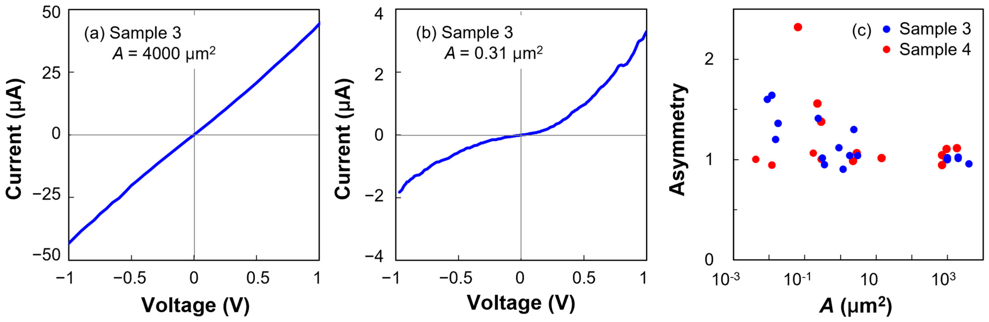
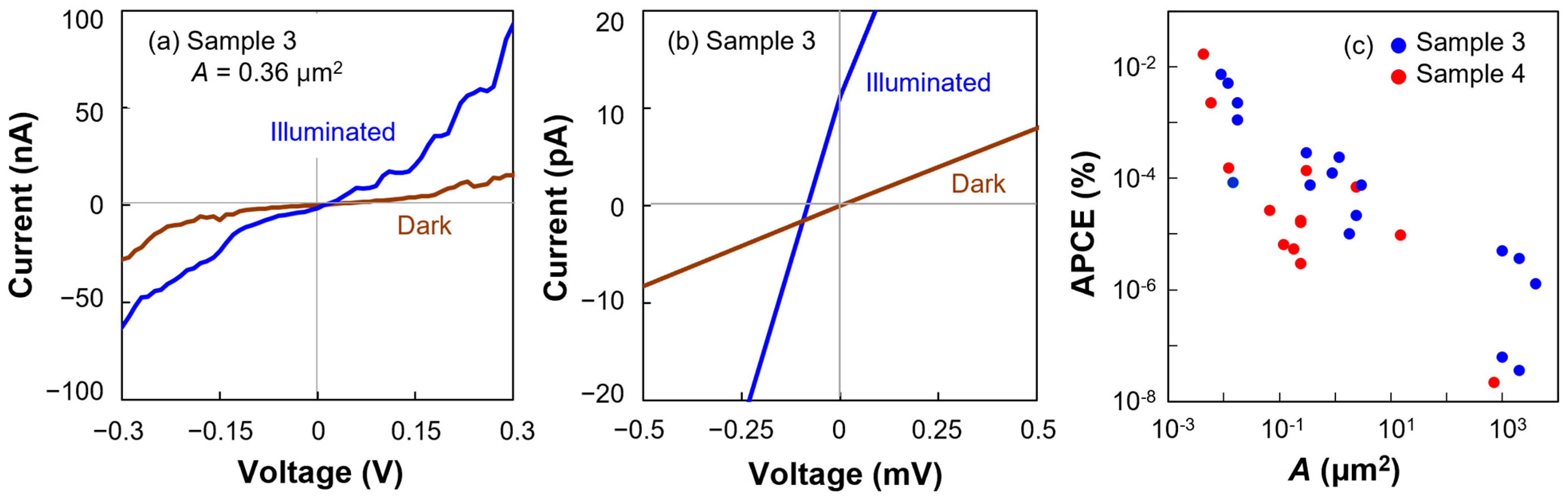
| Sample 3 | Graphene/I1/I2/Graphene | Al2O3 (2 + 3 nm)/SiO2 (3 nm) |
| Sample 4 | Graphene/I1/I2/Graphene | Al2O3 (2 + 3 nm)/SiO2 (6 nm) |
Disclaimer/Publisher’s Note: The statements, opinions and data contained in all publications are solely those of the individual author(s) and contributor(s) and not of MDPI and/or the editor(s). MDPI and/or the editor(s) disclaim responsibility for any injury to people or property resulting from any ideas, methods, instructions or products referred to in the content. |
© 2026 by the authors. Licensee MDPI, Basel, Switzerland. This article is an open access article distributed under the terms and conditions of the Creative Commons Attribution (CC BY) license.
Share and Cite
Uchino, T.; Heng, Y.; Tang, C.; Satou, A.; Fukidome, H.; Otsuji, T. Rectifying and Photoconductive Responses in Graphene–Double-Insulator–Graphene (GI2G) Structures. C 2026, 12, 18. https://doi.org/10.3390/c12010018
Uchino T, Heng Y, Tang C, Satou A, Fukidome H, Otsuji T. Rectifying and Photoconductive Responses in Graphene–Double-Insulator–Graphene (GI2G) Structures. C. 2026; 12(1):18. https://doi.org/10.3390/c12010018
Chicago/Turabian StyleUchino, Takashi, Yanjun Heng, Chao Tang, Akira Satou, Hirokazu Fukidome, and Taiichi Otsuji. 2026. "Rectifying and Photoconductive Responses in Graphene–Double-Insulator–Graphene (GI2G) Structures" C 12, no. 1: 18. https://doi.org/10.3390/c12010018
APA StyleUchino, T., Heng, Y., Tang, C., Satou, A., Fukidome, H., & Otsuji, T. (2026). Rectifying and Photoconductive Responses in Graphene–Double-Insulator–Graphene (GI2G) Structures. C, 12(1), 18. https://doi.org/10.3390/c12010018