Article

Gate-Tunable Asymmetric Quantum Dots in Graphene-Based Heterostructures: Pure Valley Polarization and Confinement

by
Adel Belayadi
1,2,*,†,‡ and
Panagiotis Vasilopoulos
3,‡
1
Ecole Supérieure des Sciences des Aliments et des Industries Agroalimentaires, ESSAIA, El Harrach 16200, Algeria
2
Department of Physics, University of Science and Technology Houari Boumediene, Bab-Ezzouar 16111, Algeria
3
Department of Physics, Concordia University, 7141 Sherbrooke Ouest, Montréal, QC H4B 1R6, Canada
*
Author to whom correspondence should be addressed.
Current address: Department of Theoretical Physics, University of Science and Technology Houari Boumediene, Bab-Ezzouar 16111, Algeria.
These authors contributed equally to this work.
Submission received: 15 January 2024 / Revised: 24 April 2024 / Accepted: 27 April 2024 / Published: 8 May 2024
(This article belongs to the Section Carbon Skeleton)

Abstract

:
We explore the possibility of attaining valley-dependent tunnelling and confinement using proximity-induced spin-orbit couplings (SOCs) in graphene-based heterostructures. We consider gate-tunable asymmetric quantum dots (AQDs) on graphene heterostructures and exhibiting a C 3 v and/or C 6 v symmetry. By employing a tight-binding model, we explicitly reveal a pure valley confinement and valley signal in AQDs by streaming the valley local density, leading to valley-charge separation in real space. The confinement of the valley quasi-bound states is sensitive to the locally induced SOCs and to the spatial distribution of the induced AQDs; it is also robust against on-site disorder. The adopted process of attaining a pure valley-Hall conductivity and confinement with zero charge currents is expected to provide more options towards valley-dependent electron optics.

Graphical Abstract

1. Introduction

Graphene has been widely used as a vital two-dimensional (2D) material for next-generation devices due its several degrees of freedom. It is constantly used in nanoelectronics due to its high carrier mobility [1,2,3], long mean free path [4,5,6] and tunable density using external fields [7,8,9]. Graphene on realistic substrates exhibits induced proximity effects which are highly desirable for spintronics applications, due to the presence of several SOCs [10,11,12,13]. Therefore, the induced SOC terms give rise to strong spin lifetime anisotropy [14] which does allow an interesting level for manipulating the valley and spin degrees of freedom and for achieving new attractive spintronic devices. In fact, the induced/controllable spin-valley coupling is known to be one of the key features in proximity-induced SOCs that are pertinent to devices for spintronic and opto-valleytronic applications [15].
Additionally, it is strongly considered as an efficient material for valleytronic devices since its two valleys at the Dirac cones (−K and +K) constitute an additional degree of freedom that could lead to several fruitful applications. In fact, they can be used to attain valley polarization that provides valley-driven currents and encoding of the information [16,17,18]. In this context, producing valleytronic devices able to manipulate valley-polarized currents [9,19,20,21] and optoelectronic effects [22,23,24], to deal with information based on momentum space, is highly desirable.
The applicability of valleytronics might strongly rely on the assumption that valley polarization and processing can be controlled through optoelectronic access. In this case, designing new materials hosting a higher-order of valley-localized states is still promising. Instead of charge confinement, valley confinement is expected to increase the optoelectronic access and valley processing as well as attaining a valley-qubit scheme of a confined electron depending on its valley degree of freedom [25,26].
Recent advances in achieving quantum confinement in graphene-based systems have opened new paths to lifting the valley degeneracy, using graphene quantum dots (GQDs) and the induced effects by electrostatic potentials and magnetic or pseudo-magnetic fields in nanobubble QDs [9,27,28,29,30].
Although almost all interesting quantum phenomena reported in such GQDs can be well understood from a theoretical background, such engineering of strain-induced QDs remains challenging. Moreover, to our knowledge, no investigation related to valley-charge separation using induced SOCs and their related point group symmetry has been reported in GQDs.
Adopting alternative ways of making GQDs to localize valley confinement instead of charge (electron) confinement is the aim of the present work. It will become clear that lifting the valley degeneracy and obtaining valley-localized states in GQDs, induced by local proximity effects, has important advantages. In fact, the motivation of our work came from recent experimental achievements in GQDs [31,32,33] in which a voltage pulse from a scanning tunnelling microscope tip can be utilized to advantageously create AQDs at the graphene interface with several substrates, the asymmetry resulting from differences in shape and/or the number of SOC terms. Here, we report the observation of valley confinement and valley-charge separation in AQDs embedded in gate-tunable graphene/heterostructure devices. These devices exhibit C 3 v and/or C 6 v symmetry that represent, for example, graphene heterostructures with transition metal dichalcogenides (TMDs) and/or hexagonal boron nitride (hBN), respectively [10,14,34].
Figure 1 is a schematic of several circular AQDs. In general, we might define several AQDs, where the right side of the strip may contain N R Gr/hBN-like QDs ( C 6 v ) and its left side N L Gr/TMD-like QDs ( C 3 v ), placed on a graphene-like sheet with zigzag boundaries. The role of the gated QDs is to control or modulate the valley contribution to the current, as we will show in Section 3, R Q D is the radius of all QDs.
The aim of the present work is to provide a systematic analysis of the role of the proximity-induced SOCs in AQDs or SQDs, their sublattice dependence, and their influence on valley polarization (in k-space) or confinement, and on valley-dependent transport. In Section 2, we briefly present the basics of the model and in Section 3 we present the numerical results. A summary follows in Section 4.

2. Basics of the Model

Engineered QDs results, such as those shown in Figure 1, give rise to several SOC terms near the QD regions that determine the symmetry of the H C 6 v and/or H C 3 v SOC Hamiltonian. The general expression of the Hamiltonian of a QD reads [10]:
H A Q D = t i , j a i σ a j σ + b i σ b j σ + 2 i 3 i , j σ , σ λ R a i σ b j σ s ^ d i j σ , σ + i 3 3 i , j σ v i j λ I ( A ) a i σ a j σ + λ I ( B ) b i σ b j σ s ^ z σ , σ + 2 i 3 i , j σ , σ λ P I A ( A ) a i σ a j σ + λ P I A ( B ) b i σ b j σ s ^ d i j σ , σ + i Δ a i σ a i σ + b i σ b i σ s ^ z σ , σ .
Here, a i σ , a j σ ( b i σ , b j σ ) are the creation and annihilation operators for an electron at sites i and j, of sublattice A (B), and σ i , i = x , y , z denotes the Pauli matrices. The nearest neighbour hopping between sites i and j is denoted by t. The terms λ I , λ R , λ P I A and Δ denote the strength of the intrinsic, Rashba, pseudo-inversion-asymmetry SOC, and staggered potential, respectively. We denote by d i , j ( D i , j ) the unit vectors connecting site j to site i for the nearest (next-nearest) neighbours where v i j is the orientation of the hopping terms in the clockwise ( + 1 ) or counterclockwise ( 1 ) . The summation notation i , j ( i , j ) refers to the SOC for the nearest (next-nearest) neighbour.
The linearization of Equation (1) leads to an effective low-energy Hamiltonian around the K 1 and K 2 points labeled by the valley index κ = 1 and κ = + 1 , respectively. The final expression is given in the form H Q D = H k + H Δ + H R + H I [10], where:
H k = v F κ k x σ x + k y σ y s 0 ,
H Δ = Δ σ z s 0 ,
H R = λ R κ σ x s y + σ y s x s 0 ,
H I = ( κ / 2 ) λ I ( a ) σ z + σ 0 + λ I ( b ) σ z σ 0 s z .
The Fermi velocity v F is expressed in terms of the hopping t as v F = 3 a 0 t / 2 where a 0 is the lattice constant. The pseudospin is denoted by the Pauli matrices σ , and s 0 denotes the spin identity matrix.
In Equation (1) the nearest and next-nearest-neighbour SOC hoppings depend on the sublattice. In this way we distinguish the left and right QDs by the sign dependence of the SOCs. For sign ( λ I ( B ) ) sign ( λ I ( A ) ) , we have the case of C 3 v symmetry; however, for sign ( λ I ( B ) ) = sign ( λ I ( A ) ) we have the case of C 6 v symmetry. For clarity we assume that all SOC terms vanish outside the QDs and are finite, staggered or not, inside them. In addition, we consider the same strength for all SOC terms in QDs with the same symmetry. The experimental feasibility of the proposed set up is discussed in a recent work [31].
To compute the valley conductance we use the Kwant package [35] which provides a key functionality to analyze and resolve the scattering matrix ( S ± κ ) in k-space channels. Within the limits of the Landauer-Büttiker approach [36], we numerically evaluate the valley-dependent conductance as
G κ n , m = ( e 2 / h ) S κ n , m 2 , ( m , n L , R ) ,
where S κ n , m is the valley scattering matrix between the left (L) (right (R)) and right (R) (left (L)) leads for a given valley index κ = ± 1 . Further details are given in Appendix A.

3. Results and Discussion

Below we present numerical results for the valley-polarized conductance in a system containing several QDs. To show its dependence on the sublattice nature and the signs of the SOCs we consider one sublattice with C 3 v symmetry (staggered SOC, sign ( λ I ( B ) ) sign ( λ I ( A ) ) ) and one with C 6 v symmetry (unresolved SOC, sign ( λ I ( B ) ) = sign ( λ I ( A ) ) ). We will investigate two cases: (1) AQDs with C 3 v and C 6 v symmetries, separated by a distance D Q D , and (2) SQDs with only C 3 v symmetry, separated by a distance D Q D , and SOCs staggered on both sides. The distance between the rightmost dot on the left side and the leftmost dot on the ride side is D L R . The results obtained are summarized in Figure 2, Figure 3, Figure 4 and Figure 5.

3.1. Valley Dependence in Gated Symmetric or Asymmetric QDs

We consider injected carriers scattered by induced QDs of radius R Q D = 7 (nm); the inter-dot distance between left and right QDs leads is D L R = 4 R Q D . The graphene width is set to W = 30 (nm) and the Fermi energy to E F = 0.035 t , and t = 1 eV.
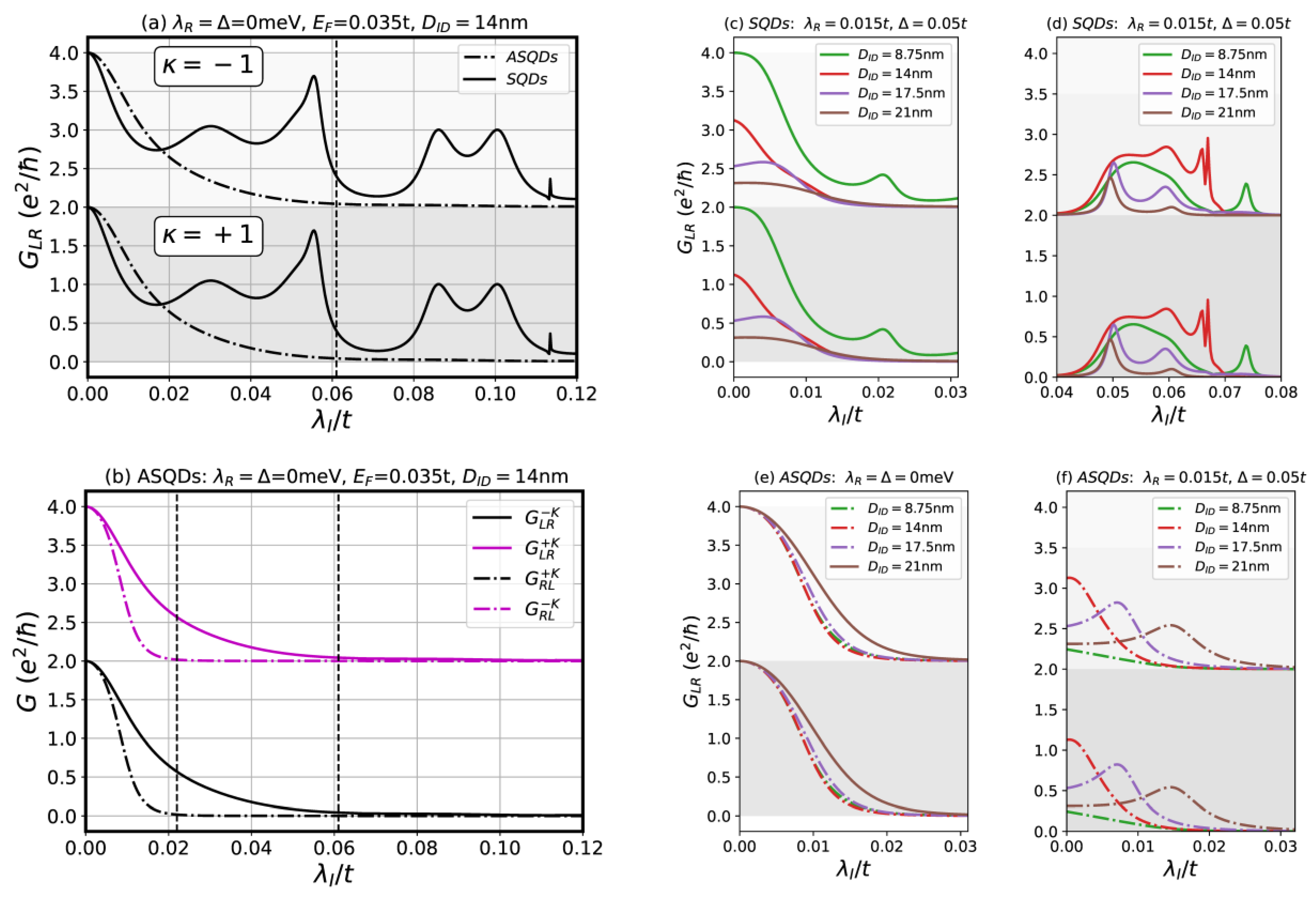
The results related to SQDs, defined by the staggered SOC parameters over all scattering regions, show that the valley conductance G is not purely polarized for weak spin-orbit range when the system has more than one valley (solid line in Figure 2a). Additionally, we observe that G, as a function of the strength λ I of the ISOC, shows a nearly square-wave transmission shown by the red solid line in Figure 2e, but without a pure valley transmittance since both valleys are conducting. In contrast, for AQDs, G shows a more robust control of its polarization. The conductance G, shown by the black dash-dotted curve in Figure 2a, displays a smooth response and decays exponentially with λ I . For instance, at weak SOC strength ( λ I = 0.06 t ), we observe a full polarization: the injected carriers exit the structure with a polarized transmission ( G L R K = 1 ; G L R + K = 0 , in units of e 2 / ) at positive energy. Obviously, AQDs are a better choice for lifting the valley degeneracy. We clearly observe that the system blocks one valley as the carriers cross the two groups of QDs.
Additionally, it is worth discussing the valley asymmetry while computing the conductance depending on the current direction. In fact, since we are dealing with AQDs, one expects that the valley selectivity, when injecting the current from right to left ( G R L ), instead of left to right ( G L R ), changes and so does the valley-dependent conductance. As shown in Figure 2b, a change in the direction of the current for the same energy leads to an exchange of the valleys. According to Figure 2b, we discuss two cases that provide valley exchange but with different polarizations depending on the value of SOC and the chosen direction of the current.
  • At λ I = 0.06 t , with the current injected from left to right, valley +K is conducting while valley −K is not. Instead, if the current is injected front the right, the conductance through valley +K vanishes and that from valley −K is finite;
  • At λ I = 0.02 t , we state that the valley polarization is ensured only in one direction. We highlight the presence of a finite conductance of one valley only ( G R L K = 1 , G R L + K = 0 , in units of e 2 / . A change in the direction of the current for the same energy does exchange the valleys, as in (1) ( λ I = 0.06 t ) but leads to a finite, unpolarized conductance at both valleys ( G L R K = 0.5 , G L R K = 2.5 , in units of e 2 / ).
We further state that the distance D L R plays a major role in processing either valley polarization or confinement as we will show later on. It is worth stating that for shorter inter-dot distances D L R , the QDs edges are closer to each other and might provide transmittance peaks due to mode mixing from the edge-dot coupling. A proper choice of D L R would avoid the edge-dot coupling and the valley transmittance would be more stabilized. In what follows, we will consider two values of D L R , ( D L R = 4 R Q D or D L R = 8 R Q D ), which have been shown to provide different valley-centered properties, namely, valley polarization or confinement.
First, as shown in Figure 2c–f, increasing D L R entails stronger SOCs to fully attain valley polarization, which is not a good choice in our case. Based on the numerical results, the best choice to control the valley is obtained when D L R = 4 R Q D . It is clearly seen that even in the presence or absence of the RSOC and staggered potentials, if D L R = 4 R Q D = 28 (nm) a full polarization in AQDs is achieved at weak SOCs, cf. Figure 2e,f. However, for SQDs in all cases we have an unpolarized conductance, cf. Figure 2c,d.
We have discussed the valley selectivity as a function of the staggered SOCs ( λ I A , λ I B ). Since AQDs play the most important role in valley selection, it is worth providing more details about the dependence of the valley conductance, in AQDs, on the RSOC and staggered potentials.
As in the case of changing the inter-dot distance, adding a weak staggered potential does not destroy the polarizations and provides a lower value of λ I needed to polarize the conductance (Figure 3a). A better choice of the staggered potential is to have Δ < a b s ( λ I ) , see Figure 3a. To further support this claim we refer to Ref. [10] in which the effect of the staggered potential in C 3 v and C 6 v is fully discussed. We mainly summarize that, depending on whether we have Δ < or > a b s ( λ I ) , for both symmetries we have different cases: an insulating flow, for Δ < a b s ( λ I ) , and a gapped case for Δ > a b s ( λ I ) .
As a function of the RSOC strength, the valley-conductance is shown in Figure 3b. Here, we consider weaker ISOC as expected in real proximity effects. When electrons are injected with E F = 0.035 t , we observe that the RSOC can play a role in controlling the valley transmittance with the use of a top gate. One can obtain a pure valley-polarized conductance for λ R in the ranges 0.02 t λ R 0.03 t and 0 λ R 0.07 t for weak staggered coupling λ I = 0.015 t or 0.025 t , respectively. The valley transmission is G L R K = 2 , G L R + K = 0 , in units of e 2 / for positive incident energy. Both the RSOC and the staggered potential are induced by the gates and, since they do not affect the time-reversal and valley-inversion symmetries, there is no effect on the results when we reverse the current direction.
We briefly mention the emergence of resonance modes that depend on the value of E F and the strength of the ISOC. The results displayed in Figure 3c shows that a resonance appears when we increase E F . For instance, at E F = 0.05 t , a sharp resonance occurs where the mode in the peak suits particularly into the QDs. The local density of states (LDOS), per valley, near the resonance defined by λ ( E F = 0.05 t ) = 0.025 t , shows that the electrons are near entirely valley localized around the last QD, leading to a characteristic vortex pattern close to the C 3 v QD boundary. The localization is valley dependent but does not provide a good application since the second valley is spreading throughout the whole sample. Below we discuss how both valleys can be confined and the dependence of their properties on the QD shape.

3.2. Valley-Hall Signals and Valley Quasi-Bound States in AQDs

Below we emphasize how AQDs are used to obtain a valley-Hall conductivity with neutral charge currents. In more detail, we show that AQDs, with a given shape (depending closely on the number of QDs on the right side ( C 3 v ) and the distance D L R , do provide an efficient way to (i) generate a pure valley-Hall polarized conductivity and (ii) confine pure valley quasi-bound states pertinent to optoelectronic processes. We will mainly consider two different systems defined by different inter-dot distances and the propagating modes whether from left or right (asymmetry in the valley).
For instance, two AQDs, with C 3 v symmetry on the right, C 6 v symmetry on the left, and separated by an inter-dot distance, can be used to either promote valley-Hall signal or confinement. Importantly, for D L R = 4 R Q D , the system exhibits a pure valley-Hall signal when the current direction is from left to right. However, for D L R = 8 R Q D and when the current is injected in the right, the system exhibits valley quasi-bound states. To make that clear, we compute the current flow in a real-space representation by mapping both valley currents and the valley-resolved LDOS, see Appendix B. The numerical results for both cases are shown in Figure 4 and Figure 5.
As stated earlier, reversing the direction of the current does not provide the same valley selectivity for the same incident energy. In this case we search for a valley selectivity when we change E F to its negative, thus changing the particle-hole symmetry. Bear in mind that the valley symmetry is broken if we shift the current direction.
First, we look for a valley-Hall action. We consider two QDs, arranged in a chain with the same radius R Q D . The distance between the gated left and right QDs is set to D L R = 4 R Q D . We consider E F = 0.035 t and map the current for AQDs and SQDs. The results are shown in Figure 4 and allow us to clearly see the main differences between SQDs or AQDs and to answer the question of whether we obtain either both Hall and bulk conductivities or only valley-Hall signals in the system.
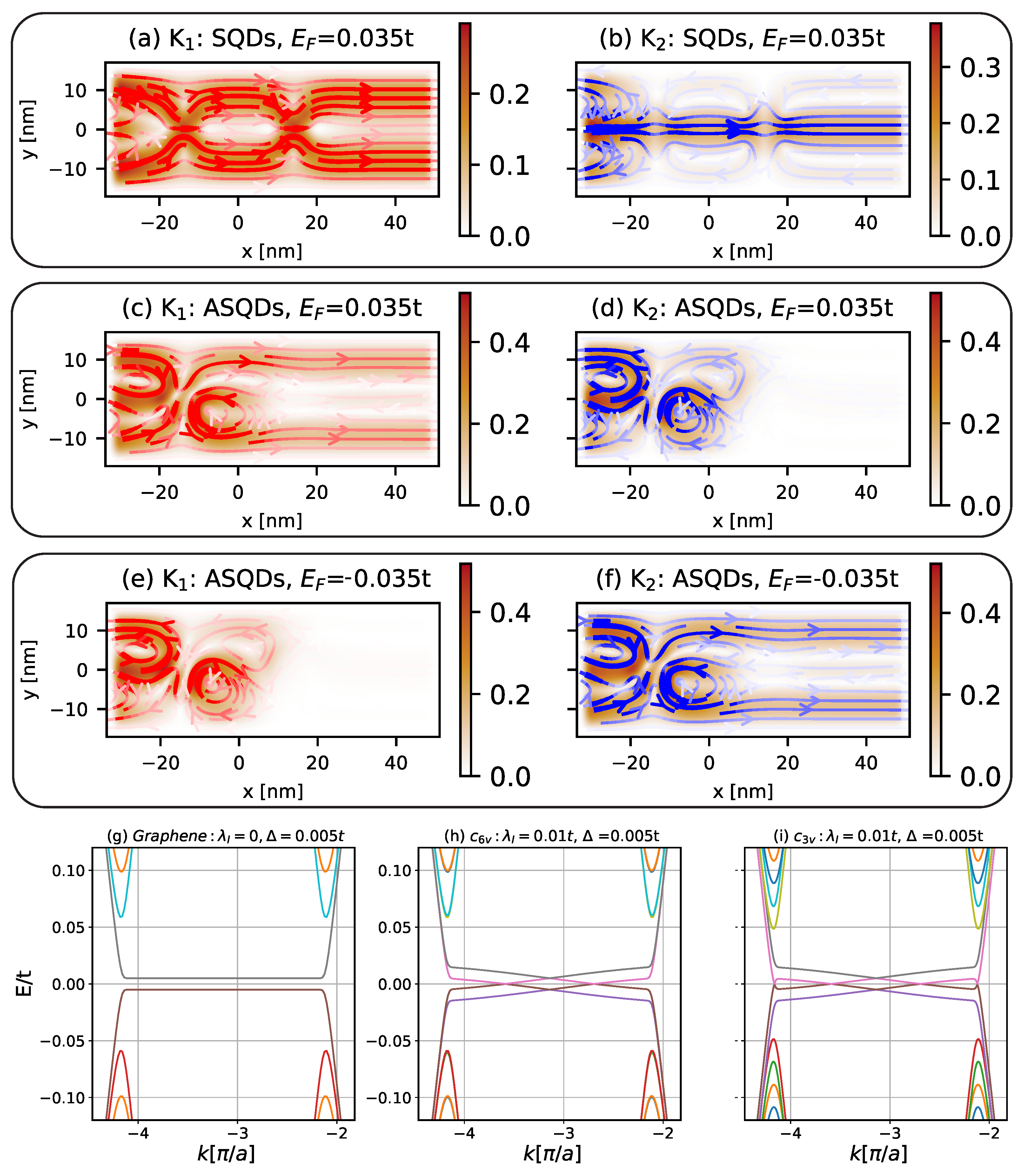
Looking at Figure 4a,b, we observe that the SQDs produce valley-Hall and -bulk signals with a charge current that is not neutral since both valleys are driving the current in the same direction (solid blue (red) curve for K 1 = −K ( K 2 = K)). However, for AQDs we see that valley-Hall signals are generated with neutral charge current, since only one valley contributes to the current while the other does not, cf. Figure 4c,d. Additionally, changing E F from positive to negative, as shown in Figure 4e,f, provides equal Hall currents, as shown in the color bar, but interchanges the valleys that provide that current (always only one valley is allowed to flow and the other is blocked). Hence, for AQDs, the valley-filtering process is always operative and promotes valley-Hall currents. We briefly state that in such a heterostructure, which includes a staggered ISOC, pseudo-helical and valley-centered edge states were observed [14,29]. Our results endorse these claims and we might produce valley filtering or valley confinement characterized by these protected edge states. These results might be understood from the analysis of the band structure in Figure 4h,i.
From the band structure in Figure 4g–i, the lowering of the symmetry gives rise to edge states that might ply a major role in conducting Hall currents as well as confining quasi-bound states. More precisely, we observe that in the case of staggered ISOC terms we have additional symmetric edge modes that appear at K 1 and K 2 which are unique to the staggered case λ I ( A ) = λ I ( B ) since they disappear in the uniform case λ I ( A ) = λ I ( B ) . For this purpose, combining both symmetries would allow more control over valley-dependent properties such as valley-Hall signals with neutral current or pure valley confinement.
It is worth stating that it is really important to consider only one QD with C 3 v symmetry on the left side of the scattering region (the ISOC is staggered), to have a perfect valley-Hall signal. Including more QDs would create an effective inter-dot hopping process which would lead to an effective inter-dot transport between the embedded QDs and hence push the current to bend from the edge of the sample towards its bulk as shown in Figure 4a,b with two QDs separated by a distance 4 R Q D .
Second, let us now discuss valley confinement with the aim of attaining pure valley quasi-bound states in the system. We will show that this kind of confinement does not correspond to resonances with some states affected by the induced SOC and Fermi energy (as discussed in Figure 3d,e), but it is rather obtained by internal reflections between the left and right QDs and depends on the inter-dot distance D L R . This confinement resides in between the left and right QDs but not within the QDs. To search for valley localized states in the presence of AQDs, we numerically evaluated the LDOS to obtain the distance D L R for which the inter-dot hopping between right and left QDs vanishes by varying D L R . The results, for fixed R Q D , show confined valley quasi-bound states for D L R = 8 R Q D and valley-Hall currents for D L R = 4 R Q D .
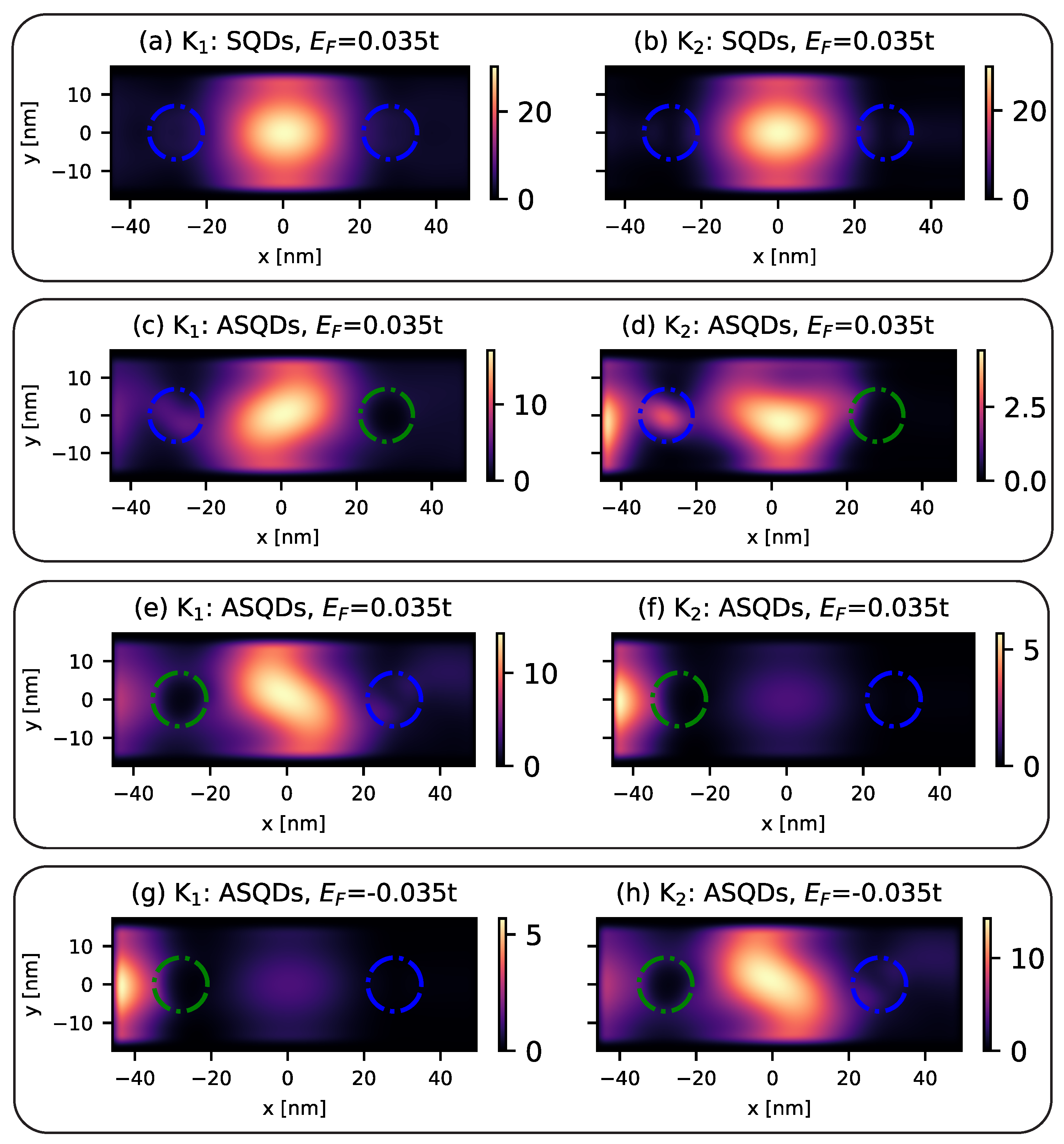
According to Figure 5a,b, for SQDs the electrons are almost completely localized between the QDs and the near absence of inter-dot hopping gives rise to vortex pattern characteristics with vortices attached to the QD boundaries. Such features (but with electron confinement) have been observed in graphene with gate-defined quantum dots [37,38]. The incident electrons are trapped without internal reflections that occur when they are confined inside the QDs [27,28]. In our case, the confinement occurs outside them, between the left and right QDs, and results from the vanishing of the inter-dot hopping when we vary D L R .
Now, when considering AQDs we may obtain results similar to those for SQDs. As shown in Figure 5c,d, when the left QD has C 3 v symmetry (blue dotted circle) and the right QD has C 6 v symmetry (green dotted circle), we have confined valley quasi-bound states but with an asymmetric distribution. However, when we change the location of the QDs (which is similar to reversing the current direction), the states in both valleys are not simultaneously confined, the confinement depends on the valley index. In this case, as shown in Figure 5d,e the pure valley-confined states are more more easily obtained using AQDs with specific shapes and point group symmetries. Altering the confinement of a given valley state is then ensured by changing the sign of E F as shown in Figure 5g,h.
The valley confinements, shown in Figure 5e–f, could be advantageous for valley optical selection. Indeed, such specific circular dots with broken inversion symmetry giving rise to confined valley quasi-bound states in a specific region, could be used to obtain a valley optical selection. The region with strong valley confinement can be optically probed and trigger valley polarization with right (left)-handed circularly polarized light. The presence of only one confined state would be coupled uniquely with either right- or left-handed polarized light.

3.3. Disorder and Robustness of the Valley Confined States

It is of interest to check the robustness of the valley-confined states in the presence of disorder. There are several types of disorder but we will consider only on-site (of strength D 0 ) and vacancy (of percentage D v ) disorder. For more details we refer to Appendix C.
From an experimental point of view, gating is used to operate valley confinement controlled by the sign of E F , as in Figure 5e,f, but it may introduce disorder to the system. In this regard, it is important to show the robustness of the valley-confined states against a disordered potential.
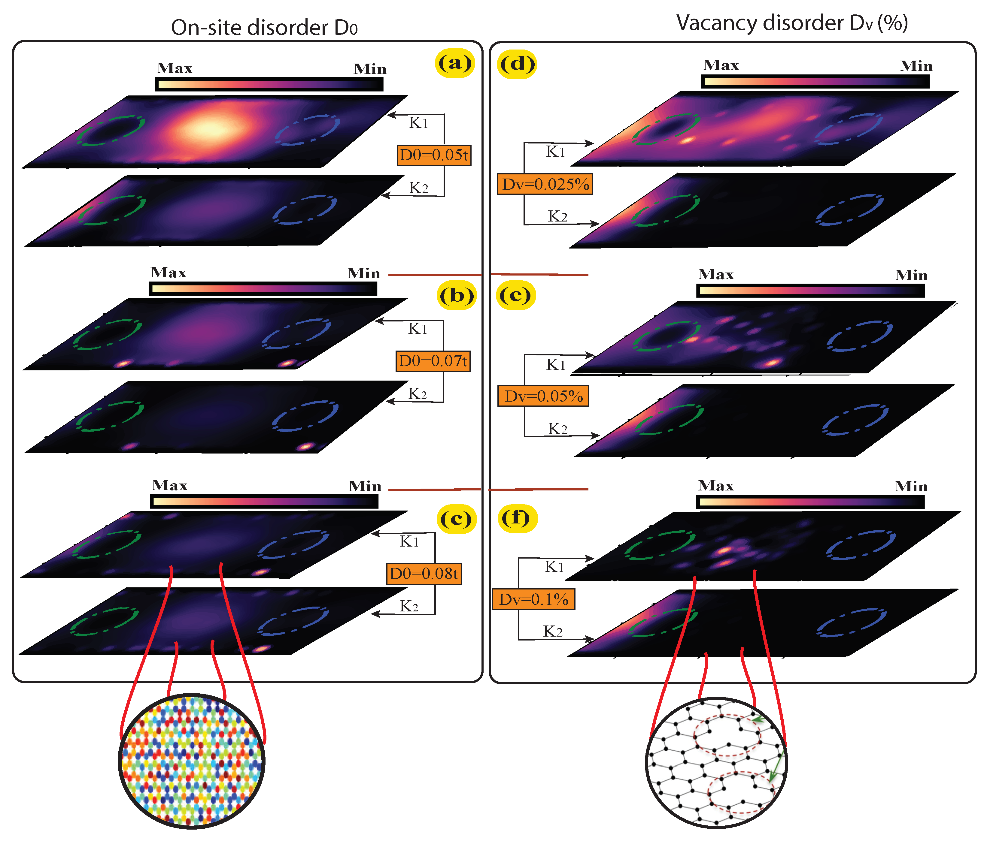
We consider an on-site disorder of strength D 0 in the range 0 t < D 0 < 0.08 t . The valley-resolved LDOS is plotted versus D 0 in Figure 6a–c.
The results show that adding a perturbative potential disorder to the system does not impact the process of confining pure valley states. For several perturbed disorder strengths, as displayed in the left part of Figure 6, we observe that a valley confinement is always present and robust against on-site disorder except when D 0 > 2 λ I . Though within limits, such a robustness against potential disorder is promising for the experimental realization of devices with applications in valleytronics and valley optical selection.
Next, it would be also interesting to consider the effect of vacancies in the sample and observe whether the confinement is affected or not. Regarding the vacancy disorder, we include the influence of vacancies in graphene sites in between the embedded QDs and consider no defect within the QDs (preserve induced proximity symmetry). We observe a behaviour similar to that of an on-site potential but the results are more sensitive to the strength (%) of defects. This is because vacancies in the lattice would generally confine the carriers around them. The results plotted in Figure 6d–f show that the valley confinement is sensitive to the defect compared to the potential disorder. A vacancy disorder larger than 0.05 % could destroy the confinement process in the sample.

4. Summary

Using a tight-binding formalism we investigated the possibility of achieving valley-dependent tunnelling and confinement using proximity-induced SOCs in graphene-based heterostructures with gate-tunable QDs. We showed that AQDs, with C 3 v and C 6 v symmetries, lead to a direct control over the valley driven current with some sensitivity to the model parameters. The results emphasized that AQDs might allow a valley selection of the current though the charge current is neutral. As such, they can provide an efficient way to generate a (1) pure valley-Hall polarized conductivity or (2) confine pure valley quasi-bound states. Indeed, the shape of the system, defined by the space in-between the left and right QDs (or the distance, D L R ) plays a major role in dealing with either option (1) or (2). A valley-Hall current is ensured, in the presence of asymmetric QDs, with inter-dot distance D L R = 4 R Q D and quantum confinement of the valley quasi-bound states for D L R = 8 R Q D .
In addition, we took into account the effect of disorder and showed that the valley-confined states are robust against on-site disorder but less so against a weak impurity disorder due to vacancies in graphene. We also presented a mechanism for obtaining valley-Hall conductivity, with valley-neutral currents, and sustaining pure valley-Hall signals or valley confinement. The main features for achieving these goals were specified. One, however, could consider a non-linear valley-Hall effect [39,40], arising from contrasting Berry curvatures and inversion symmetry breaking, that may provide even richer results. Such considerations will be addressed in future work.
Our work emphasizes that valley-centered properties are sensitive to the locally induced SOCs. Indeed, with an appropriate choice of the proximity effects, one might process and attain a pure valley-Hall conductivity and confinement with zero charge currents. This provides more options towards valley-dependent features.
In summary, combining AQDs with C 3 v and C 6 v symmetries in QDs on graphene does provide an alternative option for creating valley-polarized currents and valley optical selection that could be useful in valley-dependent electron optics.

Author Contributions

A.B. Conceptualization; Investigation; Methodology; P.V. Investigation, Writing—review & editing. All authors have read and agreed to the published version of the manuscript.

Funding

This research received no external funding.

Data Availability Statement

The data that support the findings of this study are available upon reasonable request from the authors.

Acknowledgments

The authors acknowledge computing time on the supercomputers at the Centre for Research in Molecular Modeling (CERMM), Richard J. Renaud Science Complex, Concordia University.

Conflicts of Interest

The authors declare no conflicts of interest.

Appendix A. Valley-Dependent Conductance

Below we outline the derivation of the valley-dependent conductance. To derive the scattering matrix with a given valley channel [41], we define the propagating modes in the leads depending on their velocity and momentum direction using the Kwant package [35]. We consider only propagating states for which Φ ( v < 0 ) . These states have both spin and valley degrees of freedom. We focus on the valley degree and lift the valley dependence by defining the propagating wave functions Φ K = Φ ( k < 0 ) , Φ K = Φ ( k > 0 ) . These wave functions resolve the scattering problem in reciprocal space, separately. Then the Green’s function formalism [42,43,44,45,46] incolves the scattering matrices S m n = S K m n + S + K m n with S ± K m n given by
S ± K m , n = Trace [ G ± K Γ m G ± K Γ n ] , ( m , n = L , R o r R , L ) ;
The Green’s function and Γ matrices are given by
G ( ϵ , ± K ) = ϵ + ι η I H A Q D ( ± K ) Σ 1
Γ = ι ( Σ Σ ) .
Γ defines the self-energy of the contact to the left and right of the scattering region and the relevant Hamiltonian is H A Q D , cf. Equation (1). Then for each valley mode the valley conductance is given, at the Dirac cones, by Equation (6).

Appendix B. Valley-Resolved Local Density of States and Current

To obtain the LDOS and current per valley we evaluate the wave functions (propagating modes) Φ . For a given translational symmetry a pair of objects contains the propagating modes at a given energy E on a single site. The propagating wave functions are therefore stored in different objects per site depending on their momentum Φ ( K ) , Φ ( K ) and their spin degree of freedom.
The resulting LDOS, at a given sample site i, is defined as
LDOS ± K E = l i | Φ l ± K 2 δ ( E E l )
where the sum is over all electron eigenstates | Φ l > = c l | 0 > of the Hamiltonian H A Q D in Equation (1) with energy E l . Separating the stored pair of objects with either positive or negative momentum leads to separate valley-dependent eigenstates by Φ ( ± K ) and hence to a valley-resolved LDOS in Equation (A4); it is calculated using Chebyshev polynomials [47] and damping kernels [48].
The density operator and continuity equation are expressed as
ρ q ± K = a Φ * a ± K H q h Φ a ± K , ρ a ± K t b J a , b ± K = 0 .
where q refers to all sites or hoppings in the scattering region and J a b ± K is the valley-resolved current.
For a given site of density ρ a , we sum over its neighbouring sites b. Then the valley current J a b ± k takes the form
J a , b ± K = Φ * ( v < 0 ) ± K i γ H a b γ * H a γ h H a γ h H a b γ Φ * ( v < 0 ) ± K .

Appendix C. Disorder in a Tight-Binding Approach

Within the tight-binding approach, we define the disordered Hamiltonian H D to be included in the Hamiltonian given by Equation (1). The effect of vacancies (impurities) is described by H D v and that of the on-site disorder H D 0 given as
H D v = D v i , j d i d i δ i d i c i + H . c + H . c ) ,
H D 0 = D 0 i c i c i ,
D v and D 0 are the corresponding strengths. Further, c ( c ) is the creation (annihilation) operator of an electron in either sublattice (A) or (B) that contains the disorder. The summation for i , j goes over the nearest neighbours.

References

  1. Dean, C.R.; Young, A.F.; Meric, I.; Lee, C.; Wang, L.; Sorgenfrei, S.; Watanabe, K.; Taniguchi, T.; Kim, P.; Shepard, K.L.; et al. Boron nitride substrates for high-quality graphene electronics. Nat. Nanotechnol. 2010, 5, 722. [Google Scholar] [CrossRef] [PubMed]
  2. Fu, W.; Nef, C.; Tarasov, A.; Wipf, M.; Stoop, R.; Knopfmacher, O.; Weiss, M.; Calame, M.; Schönenberger, C. High mobility graphene ion-sensitive field-effect transistors by noncovalent functionalization. Nanoscale 2013, 5, 12104. [Google Scholar] [CrossRef] [PubMed]
  3. Banszerus, L.; Schmitz, M.; Engels, S.; Dauber, J.; Oellers, M.; Haupt, F.; Watanabe, K.; Taniguchi, T.; Beschoten, B.; Stampfer, C. Ultrahigh-mobility graphene devices from chemical vapor deposition on reusable copper. Sci. Adv. 2015, 1, e1500222. [Google Scholar] [CrossRef] [PubMed]
  4. Tse, W.K.; Hwang, E.H.; Sarma, S.D. Ballistic hot electron transport in graphene. Appl. Phys. Lett. 2008, 93, 023128. [Google Scholar] [CrossRef]
  5. Masubuchi, S.; Iguchi, K.; Yamaguchi, T.; Onuki, M.; Arai, M.; Watanabe, K.; Taniguchi, T.; Machida, T. Boundary Scattering in Ballistic Graphene. Phys. Rev. Lett. 2012, 109, 036601. [Google Scholar] [CrossRef]
  6. Singh, A.K.; Auton, G.; Hill, E.; Song, A. Estimation of intrinsic and extrinsic capacitances of graphene self-switching diode using conformal mapping technique. 2D Mater. 2018, 5, 035023. [Google Scholar]
  7. Mahmud, M.T.; Sandler, N. Emergence of strain-induced moiré patterns and pseudomagnetic field confined states in graphene. Phys. Rev. B 2020, 102, 235410. [Google Scholar] [CrossRef]
  8. Mahmud, M.T.; Zhai, D.; Sandler, N. Strain Modulated Superlattices in Graphene. Nano Lett. 2023, 23, 7725. [Google Scholar] [CrossRef] [PubMed]
  9. Hadadi, N.; Belayadi, A.; AlRabiah, A.; Ly, O.; Akosa, C.A.; Vogl, M.; Bahlouli, H.; Manchon, A.; Abbout, A. Pseudo electric field and pumping valley current in graphene nanobubbles. Phys. Rev. B 2023, 108, 195418. [Google Scholar] [CrossRef]
  10. Tobias, F.; Petra, H.; Martin, G.; Denis, K.; Jaroslav, F. Protected Pseudohelical Edge States in Z2-Trivial Proximitized Graphene. Phys. Rev. Lett. 2018, 120, 156402. [Google Scholar]
  11. Petra, H.; Tobias, F.; Zollner, K.; Denis, K.; Martin, G.; Jaroslav, F. Quantum Anomalous Hall Effects in Graphene from Proximity-Induced Uniform and Staggered Spin-Orbit and Exchange Coupling. Phys. Rev. Lett. 2020, 124, 136403. [Google Scholar]
  12. Belayadi, A.; Vasilopoulos, P. A spin modulating device, tuned by the Fermi energy, in honeycomb-like substrates periodically stubbed with transition-metal-dichalkogenides. Nanotechnology 2023, 34, 085704. [Google Scholar]
  13. Belayadi, A.; Vasilopoulos, P. Spin-dependent polarization and quantum Hall conductivity in decorated graphene: Influence of locally induced spin–orbit-couplings and impurities. Nanotechnology 2023, 34, 365706. [Google Scholar] [CrossRef]
  14. Ghiasi, T.S.; Ingla-Aynés, J.; Kaverzin, A.A.; van Wees, B.J. Large Proximity-Induced Spin Lifetime Anisotropy in Transition-Metal Dichalcogenide/Graphene Heterostructures. Nano Lett. 2017, 17, 7528–7532. [Google Scholar] [CrossRef]
  15. Cummings, A.W.; Garcia, J.H.; Fabian, J.; Roche, S. Giant Spin Lifetime Anisotropy in Graphene Induced by Proximity Effects. Phys. Rev. Lett. 2017, 119, 206601. [Google Scholar] [CrossRef]
  16. Rohling, N.; Burkard, G. Universal quantum computing with spin and valley states. New J. Phys. 2012, 14, 083008. [Google Scholar] [CrossRef]
  17. Schaibley, J.R.; Yu, H.; Clark, G.; Rivera, P.; Ross, J.S.; Seyler, K.L.; Yao, W.; Xu, X. Valleytronics in 2D materials. Nat. Rev. Mater. 2016, 1, 16055. [Google Scholar] [CrossRef]
  18. Szechenyi, G.; Chirolli, L.; Palyi, A. Impurity-assisted electric control of spin-valley qubits in monolayer MoS2. 2D Mater. 2018, 5, 035004. [Google Scholar] [CrossRef]
  19. Krasnok, A.; Alù, A. Valley-Selective Response of Nanostructures Coupled to 2D Transition-Metal Dichalcogenides. Appl. Sci. 2018, 7, 1157. [Google Scholar] [CrossRef]
  20. Sharma, S.; Elliott, P.; Shallcross, S. Valley control by linearly polarized laser pulses. Optica 2022, 9, 947. [Google Scholar] [CrossRef]
  21. Godiksen, R.H.; Wang, S.; Raziman, T.V.; Rivas, J.G.; Curto, A.G. Impact of indirect transitions on valley polarization in WS2 and WSe2. Nanoscale 2022, 14, 17761. [Google Scholar] [CrossRef]
  22. Qi, J.; Li, X.; Niu, Q.; Feng, J. Giant and tunable valley degeneracy splitting in MoTe2. Phys. Rev. B 2015, 92, 121403. [Google Scholar] [CrossRef]
  23. Cresti, A.; Nikolic, B.K.; Garcıa, J.H.; Roche, S. Charge, spin and valley Hall effects in disordered graphene. Riv. Del Nuovo Cim. 2016, 39, 587. [Google Scholar]
  24. Zhang, Z.; Ni, X.; Huang, H.; Hu, L.; Liu, F. Valley splitting in the van der Waals heterostructure WSe2/CrI3: The role of atom superposition. Phys. Rev. B 2019, 99, 115441. [Google Scholar] [CrossRef]
  25. Wu, Y.; Tong, Q.; Liu, G.-B.; Yu, H.; Yao, W. Spin-valley qubit in nanostructures of monolayer semiconductors: Optical control and hyperfine interaction. Phys. Rev. B 2016, 93, 045313. [Google Scholar] [CrossRef]
  26. Pawlowski, J. Spin-valley system in a gated MoS2-monolayer quantum dot. New J. Phys. 2019, 21, 123029. [Google Scholar] [CrossRef]
  27. Behn, W.A.; Krebs, Z.J.; Smith, K.J.; Watanabe, K.; Taniguchi, T.; Brar, V.W. Measuring and Tuning the Potential Landscape of Electrostatically Defined Quantum Dots in Graphene. Nano Lett. 2021, 21, 5013. [Google Scholar] [CrossRef]
  28. Belayadi, A.; Hadadi, N.; Vasilopoulos, P.; Abbout, A. Valley-dependent tunneling through electrostatically created quantum dots in heterostructures of graphene with hexagonal boron nitride. Phys. Rev. B 2023, 108, 085419. [Google Scholar] [CrossRef]
  29. Park, H.C.; Son, M.; Lee, S.J.; Myoung, N. A strain-engineered graphene qubit in a nanobubble. J. Korean Phys. Soc. 2021, 78, 1208. [Google Scholar] [CrossRef]
  30. Li, S.Y.; He, L. Recent progresses of quantum confinement in graphene quantum dots. Front. Phys. 2022, 17, 33201. [Google Scholar] [CrossRef]
  31. Ren, H.-Y.; Ren, Y.-N.; Zheng, Q.; He, J.-Q.; He, L. Electron-electron interaction and correlation-induced two density waves with different Fermi velocities in graphene quantum dots. Phys. Rev. B 2023, 108, L081408. [Google Scholar] [CrossRef]
  32. Miravet, D.; Altıntaş, A.; Rodrigues, A.W.; Bieniek, M.; Korkusinski, M.; Hawrylak, P. Interacting holes in gated WSe2 quantum dots. Phys. Rev. B 2023, 108, 195407. [Google Scholar] [CrossRef]
  33. Boddison-Chouinard, J. Gate-controlled quantum dots in monolayer WSe2. Appl. Phys. Lett. 2021, 119, 133104. [Google Scholar] [CrossRef]
  34. Zollner, K.; Gmitra, M.; Fabian, J. Heterostructures of graphene and hBN: Electronic, spin-orbit, and spin relaxation properties from first principles. Phys. Rev. B 2019, 99, 125151. [Google Scholar] [CrossRef]
  35. Groth, C.W.; Wimmer, M.; Akhmerov, A.R.; Waintal, X. Kwant: A software package for quantum transport. New J. Phys 2014, 16, 063065. [Google Scholar] [CrossRef]
  36. Datta, S. Electronic Transport in Mesoscopic Systems; Cambridge University Press: Cambridge, UK, 1995. [Google Scholar]
  37. Heinisch, R.L.; Bronold, F.X.; Fehske, H. Mie scattering analog in graphene: Lensing, particle confinement, and depletion of Klein tunneling.Mie scattering analog in graphene: Lensing, particle confinement, and depletion of Klein tunneling. Phys. Rev. B 2013, 87, 155409. [Google Scholar] [CrossRef]
  38. Fehske, H.; Hager, G.; Pieper, A. Electron confinement in graphene with gate-defined quantum dots. Phys. Status Solidi B 2015, 252, 1868. [Google Scholar] [CrossRef]
  39. Das, K.; Ghorai, K.; Culcer, D.; Agarwal, A. Nonlinear Valley Hall Effect. Phys. Rev. Lett. 2024, 132, 096302. [Google Scholar] [CrossRef] [PubMed]
  40. Lihm, J.-M.; Park, C.-H. Nonlinear Hall Effect from Long-Lived Valley-Polarizing Relaxons. Phys. Rev. Lett. 2024, 132, 106402. [Google Scholar] [CrossRef] [PubMed]
  41. Nedell, J.G.; Spector, J.; Abbout, A.; Vogl, M.; Fiete, G.A. Deep learning of deformation-dependent conductance in thin films: Nanobubbles in graphene. Phys. Rev. B 2022, 105, 075425. [Google Scholar] [CrossRef]
  42. Istas, M.; Groth, C.; Akhmerov, A.R.; Wimmer, M.; Waintal, X. A general algorithm for computing bound states in infinite tight-binding systems. SciPost Phys. 2018, 4, 026. [Google Scholar] [CrossRef]
  43. Ozaki, T.; Nishio, K.; Kino, H. Efficient implementation of the nonequilibrium Green function method for electronic transport calculations. Phys. Rev. B 2010, 81, 035116. [Google Scholar] [CrossRef]
  44. Belayadi, A.; Bourahla, B. A theoretical model to compute the localized electronic states at the surface of hexagonal structures with different coupling orbitals. Surf. Sci. 2018, 675, 1–14. [Google Scholar] [CrossRef]
  45. Belayadi, A.; Bourahla, B.; Mekideche-Chafa, F. Localized electronic surface states in metalic structures. Surf. Rev. Lett. 2018, 25, 1850101. [Google Scholar] [CrossRef]
  46. Blayadi, A. A phase field matching model to compute the localized electronic bands of a 3D monatomic chain of body-centered cube structure: Investigating the (100), (110) and (111) cutting directions. Physica. B. Condens. Matter 2018, 547, 12–32. [Google Scholar] [CrossRef]
  47. Ferreira, A.; Mucciolo, E. Critical Delocalization of Chiral Zero Energy Modes in Graphene. Phys. Rev. Lett. 2015, 115, 106601. [Google Scholar] [CrossRef]
  48. Weibe, A.; Wellein, G.; Alvermann, A.; Fehske, H. Alexander Weiße, Gerhard Wellein, Andreas Alvermann, and Holger Fehske. Critical Delocalization of Chiral Zero Energy Modes in Graphene. Rev. Mod. Phys. 2006, 78, 275. [Google Scholar]
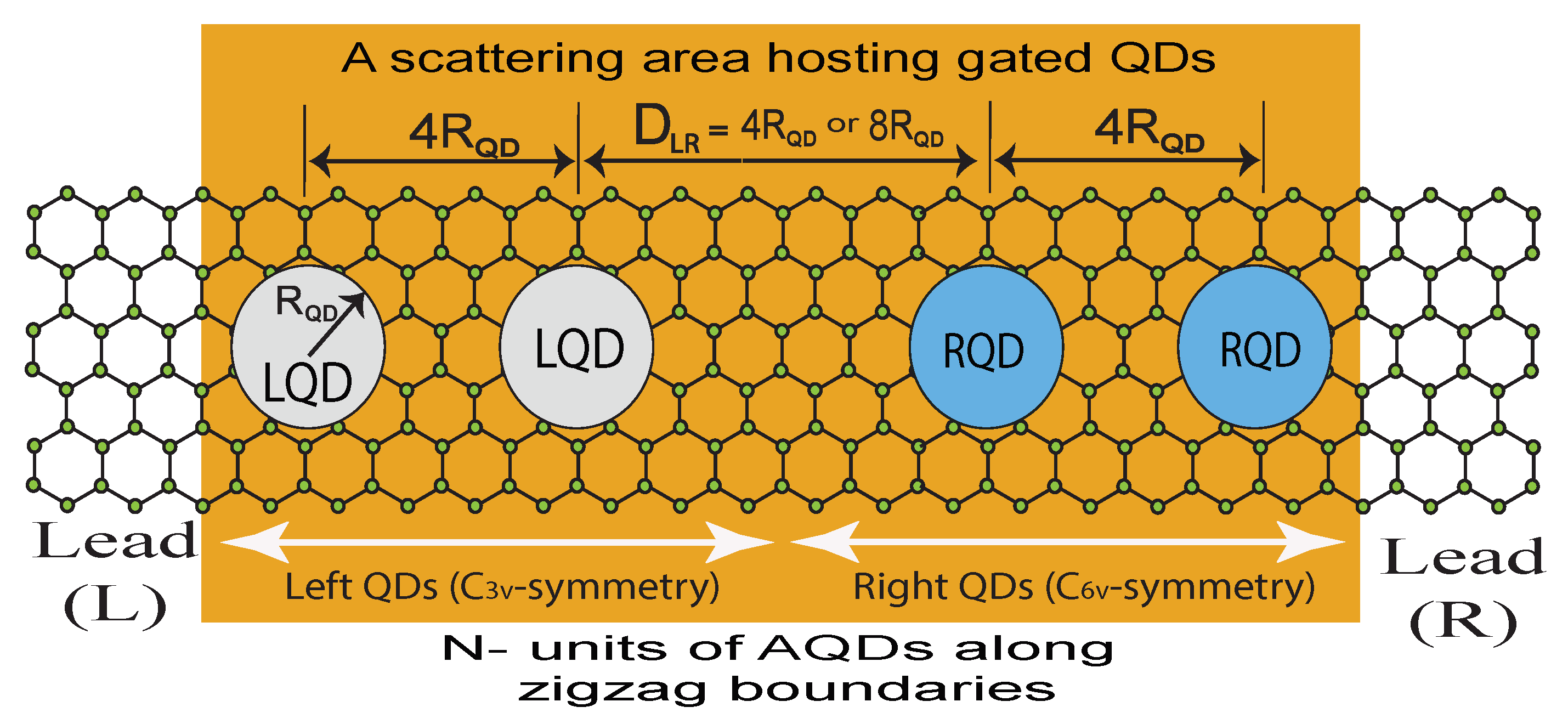
Figure 1. Schematic representation of a graphene monolayer with asymmetric quantum dots (AQDs). The left side contains light gray dots, with C 3 v or C 6 v symmetry, and the right side light blue dots with C 6 v or C 3 v symmetry. The QD radius is the same for all QDs, R Q D = 7 nm. The distance between the rightmost dot on the left side and leftmost one on the right side is denoted by D L R and that between the dots on either side is denoted by D Q D = 4 R Q D and is fixed. Due to the asymmetry in the direction of the current, we consider injected carriers from left to right ( G L R ) or from right to left ( G R L ). Injecting the current front the right is similar to injecting it from the left but with exchanged QD symmetries between left and right.
Carbon 10 00044 g001
Figure 2. (a) Valley conductance vs. intrinsic SOC length with either symmetric or asymmetric QDs. (b) As in (a) for AQDs with different propagating directions ( G L R or G R L ). Panels (cf) are zoom-ins of the indicated ranges of λ I with the effect of the inter-dot distance ( D I D = D L R ) in the presence of RSOC and staggered potentials.
Carbon 10 00044 g002
Figure 3. Valley conductance versus ISOC (for different staggered potentials in (a) and E F in (c)) or RSOC (for several ISOC strengths in (b)). Panels (d,e) show the LDOS per valley at E F = 0.05 t for staggered SOC λ I = 0.025 t .
Carbon 10 00044 g003
Figure 4. Current mapping in real space where the red (blue) lines show the valley current K 1 = K ( K 2 = + K ). Panels (a,b) are for SQDs, while (cf) are for AQDs. The current mapping is plotted at E F = ± 0.035 t for the staggered SOC λ I = 0.052 t . Panel (gi) show the energy bands, of a zigzag ribbon in case of graphene, C 6 v and C 3 v .
Carbon 10 00044 g004
Figure 5. Valley-resolved LDOS in the presence of QDs. Panels (a,b) show the LDOS of confined states for SQDs, while panels (ch) for AQDs. The blue (green) dotted circle highlights the location of the gated dots with C 3 v ( C 6 v ) symmetry. The current mapping is plotted for E F = 0.035 t and a weak staggered SOC λ I = 0.02 t .
Carbon 10 00044 g005
Figure 6. Valley resolved LDOS in the presence of QDs: as in Figure 5, but with on-site disorder included in the (left) panels and vacancy disorder in the (right) panels.
Carbon 10 00044 g006
Disclaimer/Publisher’s Note: The statements, opinions and data contained in all publications are solely those of the individual author(s) and contributor(s) and not of MDPI and/or the editor(s). MDPI and/or the editor(s) disclaim responsibility for any injury to people or property resulting from any ideas, methods, instructions or products referred to in the content.