1. Introduction
Among thin film solar cell development, both CdTe- and CuInGaSe
2 (CIGS)-based devices have taken the lead achieving ~22% conversion efficiency for laboratory scale small devices [
1,
2]. On the upscaling and commercialisation front, CdTe solar cell take the lead producing module efficiencies of over 18%. One reason is the involvement of only two elements rather than four elements in the case of CIGS.
In order to further increase the conversion efficiencies beyond ~22%, deep understanding of materials issues, processing steps, and device configurations should be improved. In the case of CdTe, the material can be easily produced as both p-type and n-type in electrical conduction, and this may directly affect the devices formed when combined with other layers such as CdS. In the past the CdS/CdTe solar cell was always assumed as a simple n-p junction and the results were analysed accordingly. However, now it is clear that n-p junctions are formed when CdTe is rich in Te and p-type electrical conduction. When the CdTe material is rich in cadmium and n-type in electrical conduction, n-n+ large Schottky barrier (SB) type devices are formed [
3]. It is also being clear that n-type CdTe material performs much better than p-type CdTe material when devices are formed [
4].
In the case of processing steps, heat treatment in the presence of CdCl2 is a crucial step in achieving high efficiencies in both cases when CdTe is p-type or n-type. The underlying mechanisms are not fully understood to date to explain why this processing step is necessary. Research is therefore necessary to unravel this important phenomenon.
Our group has proposed [
5,
6], and is now working on, next generation multilayer solar cells based on graded bandgap devices [
4,
5,
6,
7]. These devices can be built on both n-type and p-type wide bandgap window layers [
8]. Out of these, devices fabricated on p-type window layers have high potential in achieving improved device parameters. This has been experimentally demonstrated by GaAs/AlGaAs systems achieving V
oc ~1.175 mV and FF ~0.86 [
9]. Our current efforts are focused on developing these devices using low-cost and scalable electro-plated materials.
In this work, Mg incorporation in CdTe was explored. Main reason is that MgTe has the ideal lattice matching to CdTe, and it is a wide bandgap (~3.00 eV) p-type material. Previous works were carried out regarding Mg inclusion to CdTe, mainly using epitaxial growth techniques, where bandgap tuning with the increment of Mg composition has been demonstrated [
10,
11,
12]. This is the first attempt to incorporate Mg to CdTe layers using any electrochemical technique. The aim of this work is to produce a p-type and wide bandgap window material to develop CdTe-based graded bandgap devices in the future.
2. Experimental Procedure
Magnesium (Mg) inclusion to CdTe has been carried out to grow CdTe:Mg layers by gradually increasing the concentration of Mg2+ obtained from MgSO4 precursor of 99.5% purity, into a 400 mL aqueous electrolytic solution containing Cd2+ obtained from 98% pure cadmium nitrate tetrahydrate (Cd(NO3)2·4H2O) precursor and tellurium (Te) precursor prepared from acidic solution of 2 g tellurium dioxide (TeO2) of 99.99% purity. First, the aqueous electrolyte was prepared from 1.5 M Cd(NO3)2·4H2O and 0.0002 M TeO2. Then MgSO4 precursor was added gradually at concentration of 10, 20, 30, 50, and 100 ppm, up to very high (50%) Mg incorporation in the bath. Both Mg2+ and Cd2+ ion precursor solutions were electro-purified before use. All these chemical precursors have been purchased from Sigma-Aldrich Ltd. (Dorset, UK). The pH and temperature of the solution has been kept constant at 4.00 ± 0.02 and ~85 °C, respectively. The pH has been adjusted using either nitric acid or ammonium hydroxide (NH4OH). Two electrode electrodeposition techniques were used for depositing the semiconductor materials on Glass/ TEC-7 Fluorine doped tin oxide (glass/FTO) substrates having sheet resistance of ~7 Ω/square. A high purity carbon rod was used as the anode, whereas the cathode (working electrode) was prepared by attaching glass/FTO substrates to carbon rod using insulating polytetrafluoroethylene (PTFE) tape. Prior to electrodeposition (ED), the substrates were cut into 3 cm × 3 cm dimension and rinsed thoroughly with de-ionised water after washing with soap solutions using cotton buds. The samples were later dried with nitrogen gas steam. GillAC potentiostat from ACM Instruments is used as the power source for the 2-electrode ED system. The electrolytic solution was heated and stirred using a hot plate and magnetic stirrer. Moderate stirring rate has been applied to the bath throughout the electrodeposition process.
Cyclic voltammogram has been carried out to determine an estimated range of deposition potential where association of all the relevant ions (Cd, Te and Mg) take place. The deposited layers were investigated using X-ray diffraction (XRD), scanning electron microscopy (SEM), energy dispersive X-ray (EDX) spectroscopy, and X-ray photoelectron spectroscopy (XPS) for compositional, morphological, and material identification analyses. For characterising and optimising electrical and optical properties of the ED samples, photoelectrochemical (PEC) cell measurements, optical absorption using UV–Vis spectrophotometry and photoluminescence (PL) spectroscopy have been carried out.
3. Results and Discussion
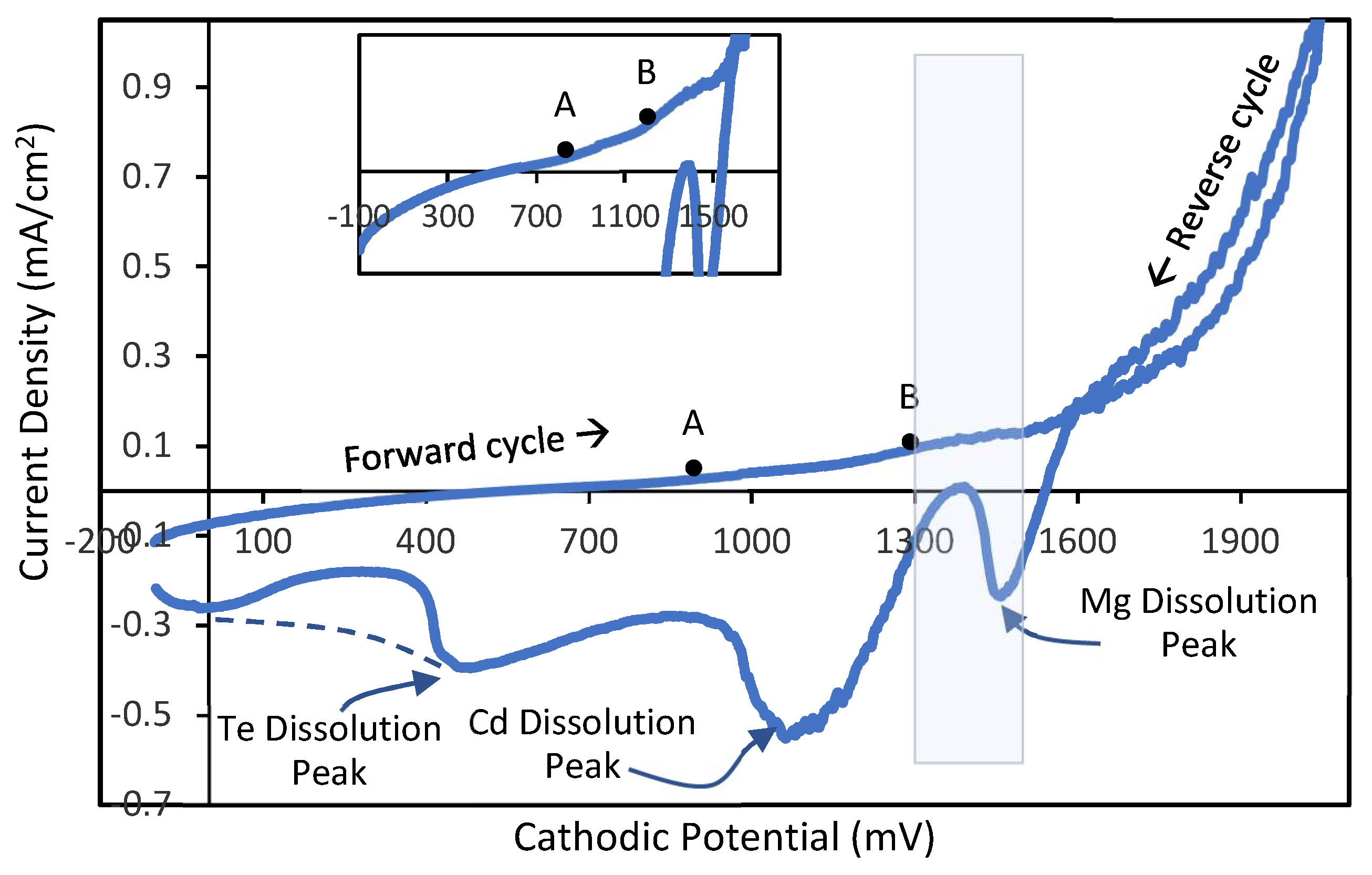
3.1. Cyclic Voltammetric Study
Cyclic voltammograms were recorded for a 400 mL electrolyte containing Cd
2+, Mg
2+, and 1 mL of TeO
2 solution. The pH and temperature of the solution is adjusted to 4.00 ± 0.02 and ~85 °C, respectively. The pH value is decided to keep at 4.00 ± 0.02 in order to reduce acidity of the electrolyte to maintain adhesion of the layer. The cyclic voltammogram was recorded with a Gill AC potentiostat from ACM instruments with a sweep rate of 3 mVs
−1 within the cathodic potential range of 0 to 2000 mV.
Figure 1 depicts a typical voltammogram data plotted with explanatory symbols and legends.
Due to the difference of redox potentials amongst the consisting ions, in the forward cycle of voltammogram Te having a redox potential (E
o) of +0.593 V (with reference to standard H
2 electrode), starts depositing at the very beginning according to the electrochemical reaction Equation (1):
Later, Cd having an E
o of −0.403 V (with reference to standard H
2 electrode) starts depositing at ~900 mV (point A in
Figure 1) according to the electrochemical reaction Equation (2):
Hence, the co-deposition of cadmium and tellurium begins hereafter and Te-rich CdTe starts to deposit from ~900 mV onward. As higher cathodic voltage is applied, Cd starts increasingly incorporating to the layer and eventually Cd-rich CdTe deposits [
13]. Then, a rise of current density at ~1250 mV (point B in
Figure 1) indicates the inclusion of Mg having an E
o of −2.372 V (with reference to standard H
2 electrode), to the deposited CdTe layer according to the electrochemical reaction Equation (3):
Therefore, from ~1250 to ~1500 mV CdTe:Mg growth takes place till the sharp increment of current density after 1500 mV, which indicates a rapid deposition of ions and possible dissociation of water. Hydrogen creation at lower level can be helpful in reduction of defects using hydrogen passivation; but rapid water splitting can be harmful for good adhesion of the layer due to hydrogen gas bubbles, thus should be avoided.
In the revers cycle of the voltammogram, the dissolution peaks indicate a similar tendency of Mg dissolving first within a range of ~1550 to ~1360 mV, Cd dissolving second in the range of ~1350 to ~900 mV, and Te dissolving at the very end of the cycle from ~900 mV downwards.
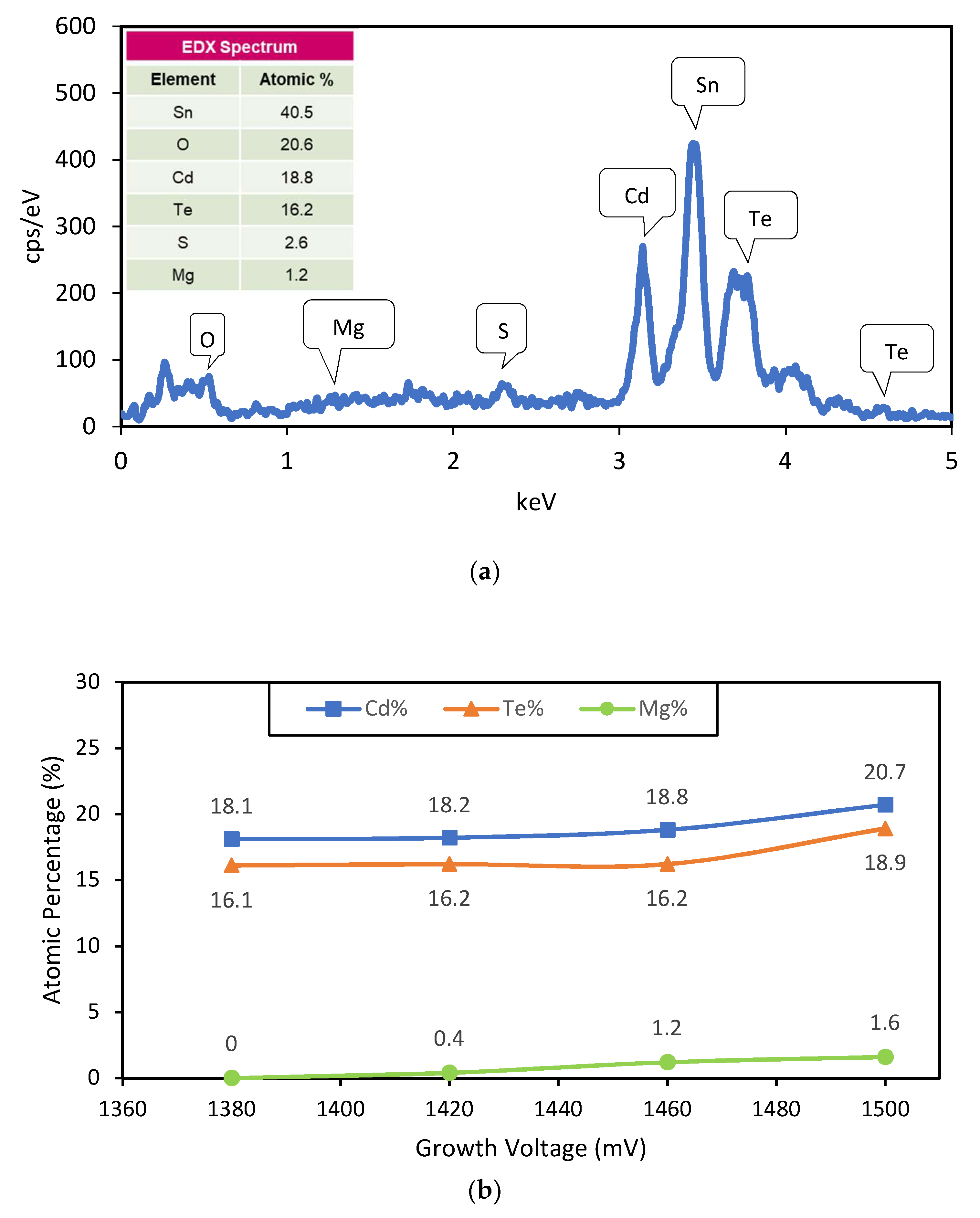
3.2. Energy Dispersive X-ray (EDX) Spectroscopy
In order to obtain the chemical composition of the samples, EDX was carried out to the as-deposited CdTe:Mg samples, using the compositional analysis software associated with the Quanta 650 SEM equipment. An EDX spectrum of the layer grown at 1460 mV is presented in the
Figure 2a.
Figure 2b presents the gradual change of atomic percentage of Cd, Te, and Mg in the as-deposited CdTe:Mg layers grown with high Mg presence in the bath at different cathodic voltages. Despite keeping the accuracy concerns of the EDX technique in mind, this analysis gives a qualitative idea about the gradual increase of Mg inclusion into the Cd-rich CdTe layer with the increment of growth voltage. The phenomenon has been further verified with XPS analysis.
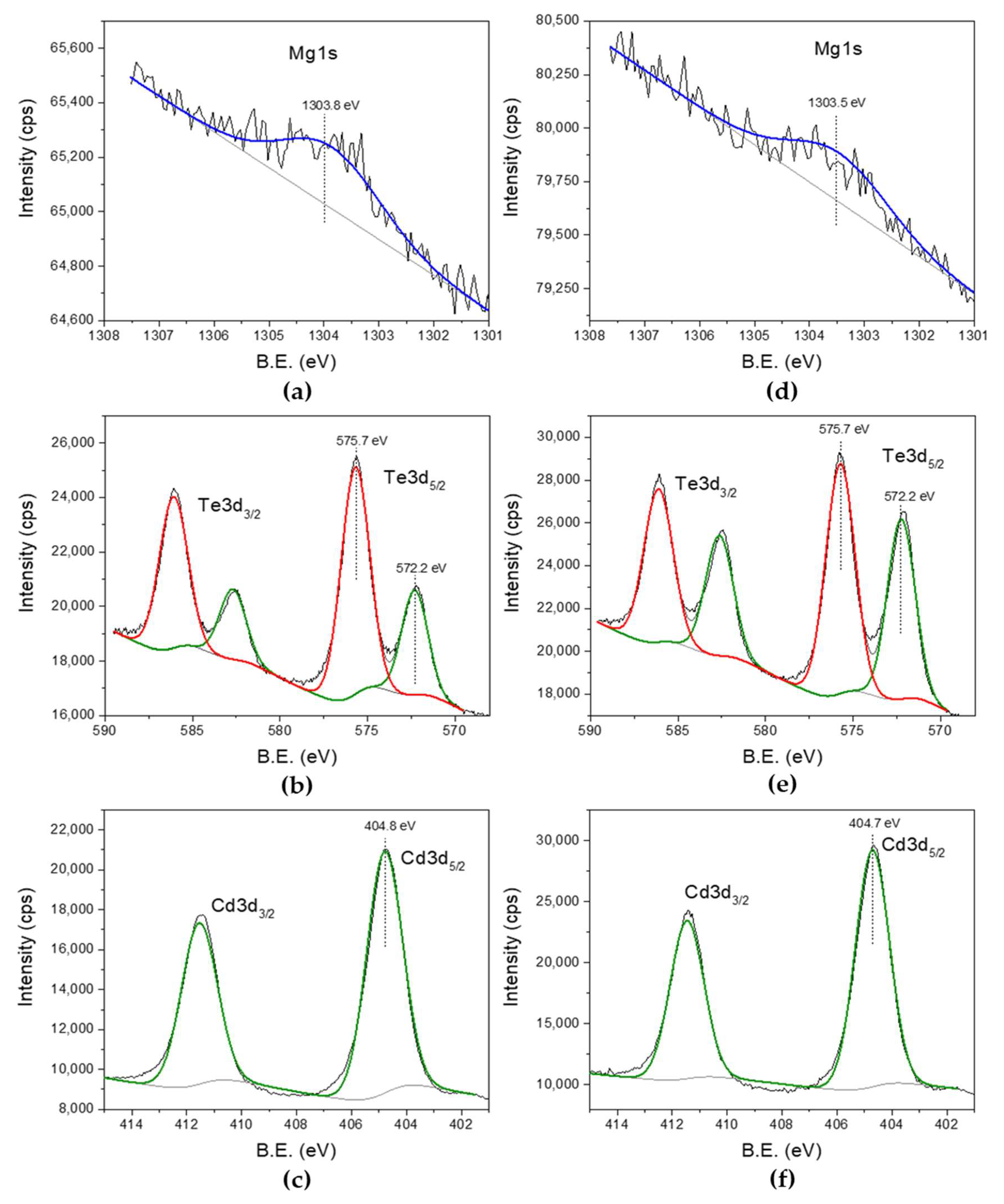
3.3. X-ray Photoelectron Spectroscopy (XPS) Analysis
X-ray photoelectron spectroscopy (XPS) measurements were performed to analyse the surface chemistry of as-deposited and heat-treated films. A VG Scientific MultiLab 3000 ultrahigh vacuum (UHV) surface analysis system, equipped with CLAM4 hemispherical electron energy analyser (Thermo Scientific, Waltham, MA, USA) and a dual-anode Mg/Al X-ray source was used for XPS measurements. All spectra were collected under the base chamber pressure in the low 10−8 Torr range using a monochromatic Al Kα (hν = 1486.6 eV) X-ray radiation. A survey spectrum from 1400 to 0 eV was collected to identify all elements. Additionally, high-resolution spectra of Mg1s, Cd3d, Te3d, and O1s were collected for elemental quantification and a high-resolution spectrum of C1s for binding energy (BE) calibration. All spectra were calibrated using adventitious C1s; C–C peak at 284.5 eV.
XPS spectroscopy of CdTe:Mg samples was carried out for as-deposited and heat-treated (HT) layers grown at 1400 mV with high Mg presence in the bath.
Figure 3a depicts an XPS peak at a binding energy of ~1303 eV, which corresponds to a typical Mg
1s orbital [
14]. This peak loses intensity after the sample is heat treated in air for 20 min at 400 °C (
Figure 3d). From
Table 1 it is further confirmed that the atomic percentage of Mg reduces due to the heat treatment, whereas the Cd and Te percentage increases in the Cd-rich sample after heat treatment.
Figure 3b,e show the high resolution Te3d peaks for as-deposited and heat-treated CdTe:Mg surface. High binding energy peak component ~3.5 eV away in the doublet clearly shows the oxidised Te on the surface. That can be due to formation of TeO
2 or Cd
xTeO
y on the surface. XRD studies on electroplated CdTe shows peaks related to Cd
xTeO
y [
7] and these peaks can be the combination of the two components TeO
2 and/or Cd
xTeO
y. Heat treatment clearly reduces the surface oxygen, indicating the evaporation or sublimation of Te-oxide components from the surface.
The strongest Cd3d5/2 peak at 404.8 eV does not show components related to CdO similar to Te. This is mainly because the binding energy of CdO is at 404.6 eV. This does not mean that Cd is not oxidised on the surface, but cannot conclude from the XPS results because of the possible overlap of the peaks.
It should be noted that the atomic percentage of elements, as detected by EDX and XPS, are different. While the EDX is detecting average values for the whole CdTe:Mg layer, the probing depth of XPS is only approximately 2–3 nm on the surface. The bulk compositions can be clearly different to the composition of the elements on the surface due to various reasons, such as evaporation and in-diffusion and out-diffusion of elements near the surface. Reduction of oxygen after heat-treatment indicates the evaporation of oxides during heating. This also explains the increase in Cd and Te atomic percentage on the surface after heat treatment.
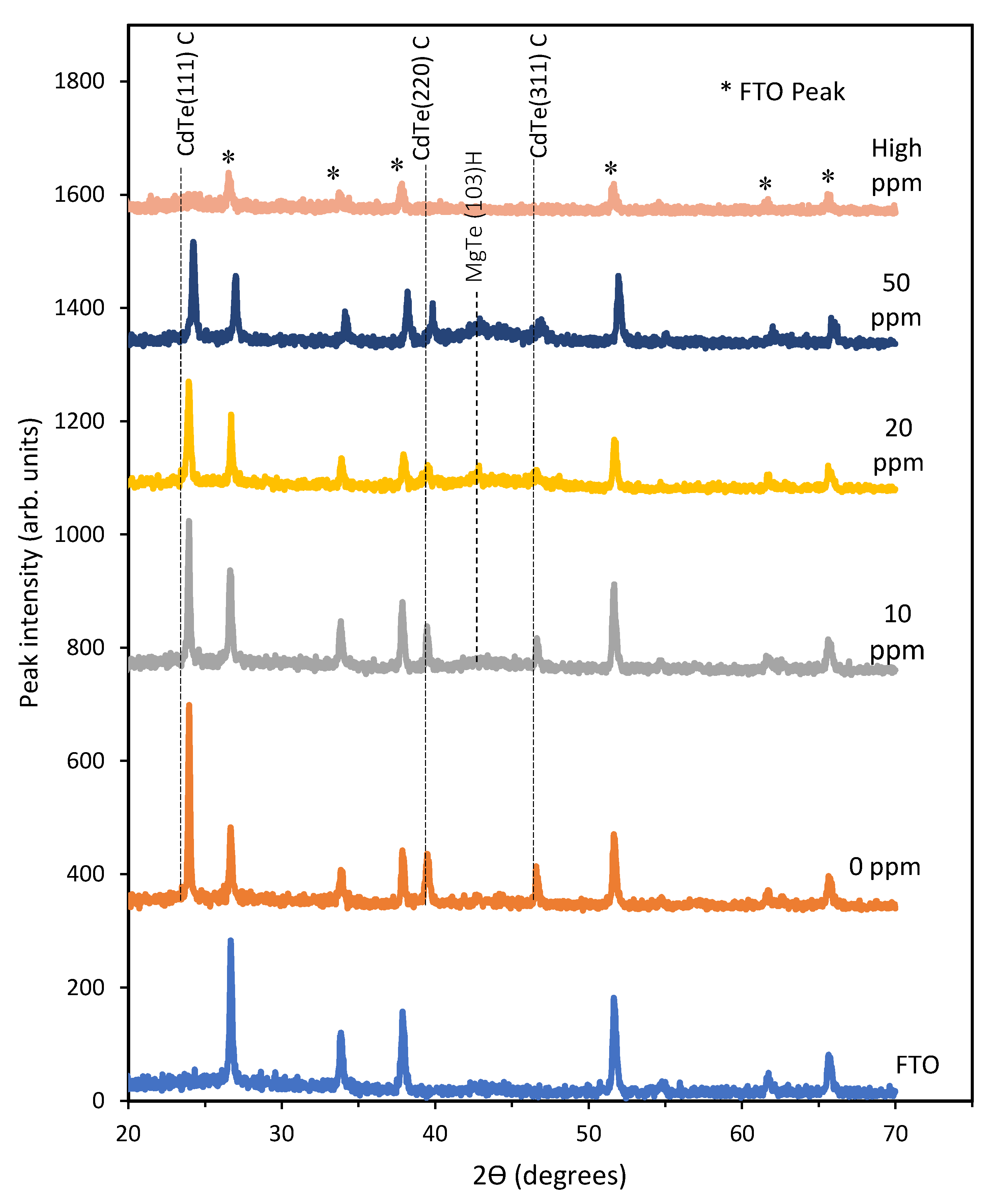
3.4. X-ray Diffraction (XRD) Spectroscopic Analysis
Aim of this analysis is to observe the change of crystallinity in the as-deposited layers of CdTe:Mg with the change of Mg inclusion in the electrolytic bath. XRD spectroscopy has been carried out on five As-deposited samples grown with electrolyte containing 0, 10, 20, and 50 ppm Mg and very high Mg inclusion in the electrolyte. A Philips PW X’Pert diffractometer (Philips, Amsterdam, Nederland) was used with a Cu-Kα monochromator of wavelength of 1.54 Å, where the source tension and current were kept as 40 kV and 40 mA, respectively. XRD scans were carried out within a range of 2θ = 20° to 70°. All the samples were grown at 1400 mV constant growth potential.
Figure 4 shows a clear gradual decrement of the CdTe (111) cubic phase in terms of XRD peak intensity at 2Ɵ ≈ 23.8°. Also, another two peaks of cubic CdTe were observed at 2Ɵ ≈ 38.9° and 2Ɵ ≈ 46.1° corresponding to the diffraction from (220) and (311) planes. Moreover, for the samples grown with 10, 20, and 50 ppm Mg in the bath, demonstrate a MgTe phase at 2Ɵ ≈ 43.1° from the (103) hexagonal plane. All these peaks also fade away with the increment of Mg inclusion in the bath.
This outcome complements the optical absorption outcome (see
Section 3.6.1) which indicated weakening of the slope steepness of absorption edge due to the introduction of possible defect states. Hence it can be assumed that the inclusion of Mg into the CdTe bath contributes not only to the formation of CdTe:Mg but also to some additional MgTe which creates possible defects in the lattice structure. Moreover, this disappearance of crystallinity of the CdTe phases can also be attributed to the competing phases of CdTe and MgTe structures. Since the reported heat of formation for MgTe (−1.08 eV/atom) is more negative than that of CdTe (−0.48 eV/atom), as soon as Mg is added to the CdTe bath, MgTe initiates to form and attempts to break the bond [
15]. As a result, CdTe:Mg layers become amorphous.
3.5. Photoelectrochemical Cell (PEC) Measurement
PEC measurements were carried out to determine the conduction type of ED layers. The measurements take the band bending that occurred due to the creation of a solid/liquid junction into account for finding out the direction of charge carriers’ flow under illuminated condition. By dipping a glass/FTO/CdTe:Mg layer along with another carbon electrode into an electrolyte prepared from 0.1M Na
2S
2O
3 (sodium thiosulphate) aqueous solution and measuring the voltage difference between the electrodes under dark (V
D) and illuminated (V
L) condition, the conduction type of the semiconductor layer is determined. The above difference in voltages provides the open circuit voltage of the solid/liquid junction or the PEC signal. For n-type semiconductors the downward band bending at the junction under dark condition enables the photogenerated electrons to flow from the liquid towards the solid and vice-versa for the p-type semiconductors. Therefore, this direction of carrier flow found from the open circuit voltage differences under two conditions (V
L–V
D) and differentiates the conduction types of the semiconductors. This voltage difference is commonly referred as the PEC signal. The setup in this work is calibrated using a glass/FTO/CdS sample beforehand, since the conduction type of CdS is always known to be n-type [
13]. For n-type layers the PEC signal is negative and for p-type it is positive for the setup used in this work, whereas for metals, insulators and intrinsic semiconductors PEC signal is ideally zero. Moreover, strength of the PEC signal qualitatively indicates to the doping density and depletion width strength.
In this work, PEC measurements have been taken for as-deposited and MgCl
2 treated samples grown with different Mg concentrations in the CdTe bath. Mg inclusion into the bath was executed in parts per million (ppm) level. Voltammetric studies have indicated the possibility of Mg inclusion in the Cd-rich CdTe layer at 1400 mV. Cd richness in the CdTe layer produces a n-type material that is likely to ensure lesser defects than that of its Te-rich p-type counterpart due to less Te precipitation [
4,
13,
16]. Therefore, the growth voltage has been kept constant at 1400 mV. All the samples were deposited on glass/FTO for two hours and were cut into two parts where one was kept as-deposited and the other was treated with MgCl
2 followed by annealing for 20 min at 400 °C in air. In
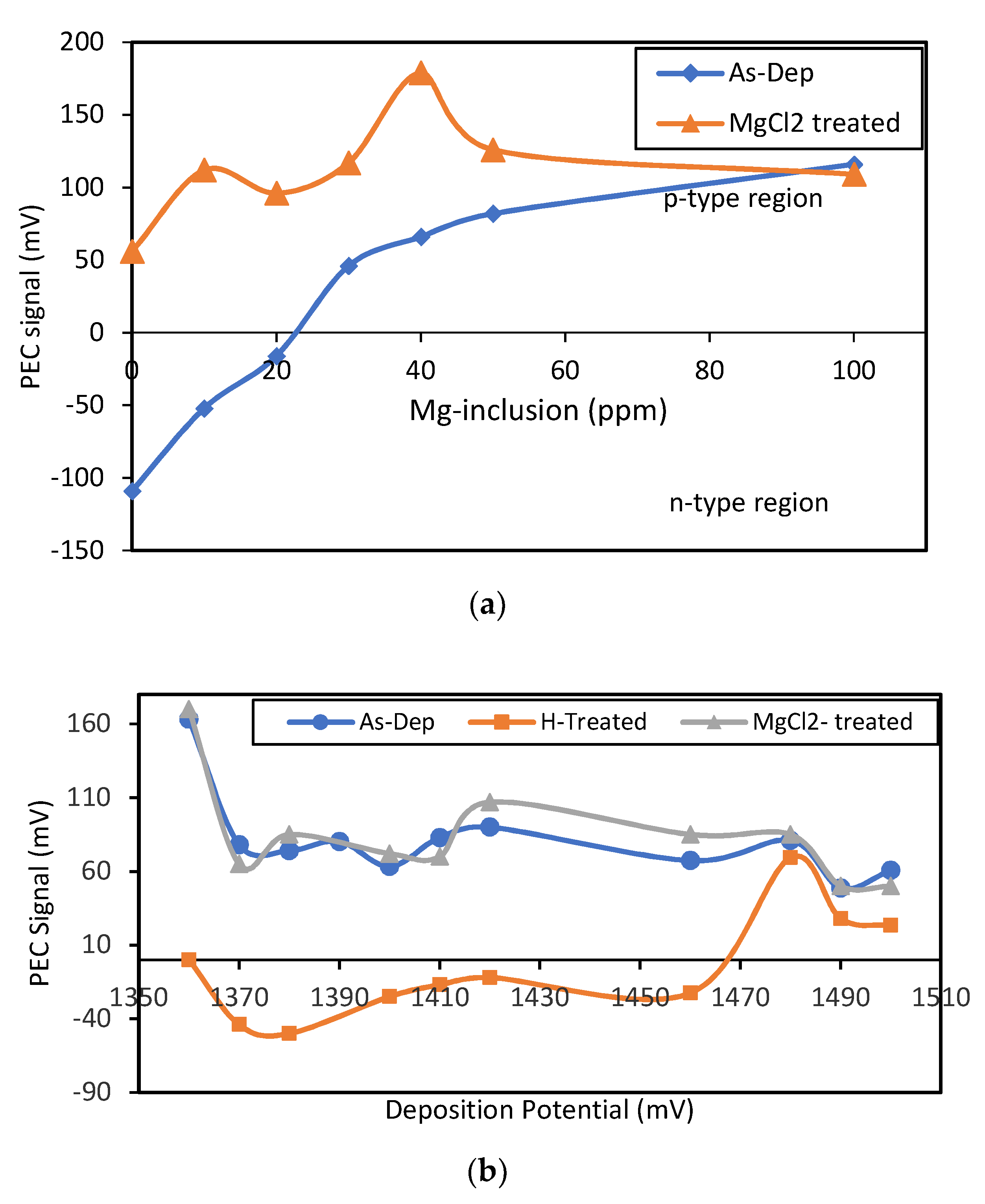
Figure 5a, the PEC signals indicate a transition of conduction type from n to p for as-deposited samples at ~25 ppm of Mg inclusion. MgCl
2 treatment (MCT) on the other hand transits the conduction type to p-type for all samples regardless of the Mg incorporation.
Higher Mg inclusion in the bath ensures the conduction type of the as-deposited layers to be p-type. Therefore, to investigate the effect of growth voltage on the layer properties, at a high stationary Mg concentration (~50%) samples were deposited within a range of 1350 to 1500 mV for two hours. Each deposited sample was divided into three parts for keeping one as-deposited, one MgCl
2 treated and the other heat treated in air at 400 °C for 20 min.
Figure 5b shows the p-type conductivity of all the AD samples, where the heat-treated (in air) samples depict an n-type conduction up to ~1460 mV. Samples deposited at ≥1480 mV maintain a p-type conductivity with slightly lower PEC signal than that of the AD samples. All the points in
Figure 5 are the average of three individual measurements.
Though Mg has a high melting point at 923 °C, but it has been seen to be evaporated at much lower temperature than that of CdTe at approximately 400 °C due to the oxidation of the layer [
17,
18,
19]. The presence of oxygen in the CdTe:Mg layers is clear from both the EDX and XPS outcomes above. Therefore, it can be assumed that evaporation of unreacted Mg due to heat treatment, leaves the CdTe:Mg layers n-type. At higher growth voltage, greater Mg inclusion enables the layers to remain p-type even after some Mg evaporation due to annealing. EDX and XPS analysis has shown a tendency consistent to it. This assumption holds true since all the MgCl
2 treated samples stay p-type even after the heat treatment at 400 °C for 20 min. This denotes that the treatment not only contributes more Mg to the layer, but also binds the Mg chemically within the structure.
3.6. Bandgap Analysis
3.6.1. Optical Absorption Analysis
The as-deposited CdTe:Mg layers grown with varying Mg presence in the bath at a constant cathodic voltage of 1400 mV for 2 h, were investigated for optical absorption studies using Carry 50 scan UV–Vis Spectrophotometer (Varian, California, USA). The optical absorption data collected within the wavelength range of 300 to 1000 nm have been used to plot-square of absorbance (
a2) vs photon energy (
hv) graph that is frequently used as an alternative to Tauc plot [
7,
20]. The curve retrieved from the graph has been used to find the direct band-gap of the deposited material by fitting tangent line to it, extrapolation of which intersects the photon energy at band-gap point.
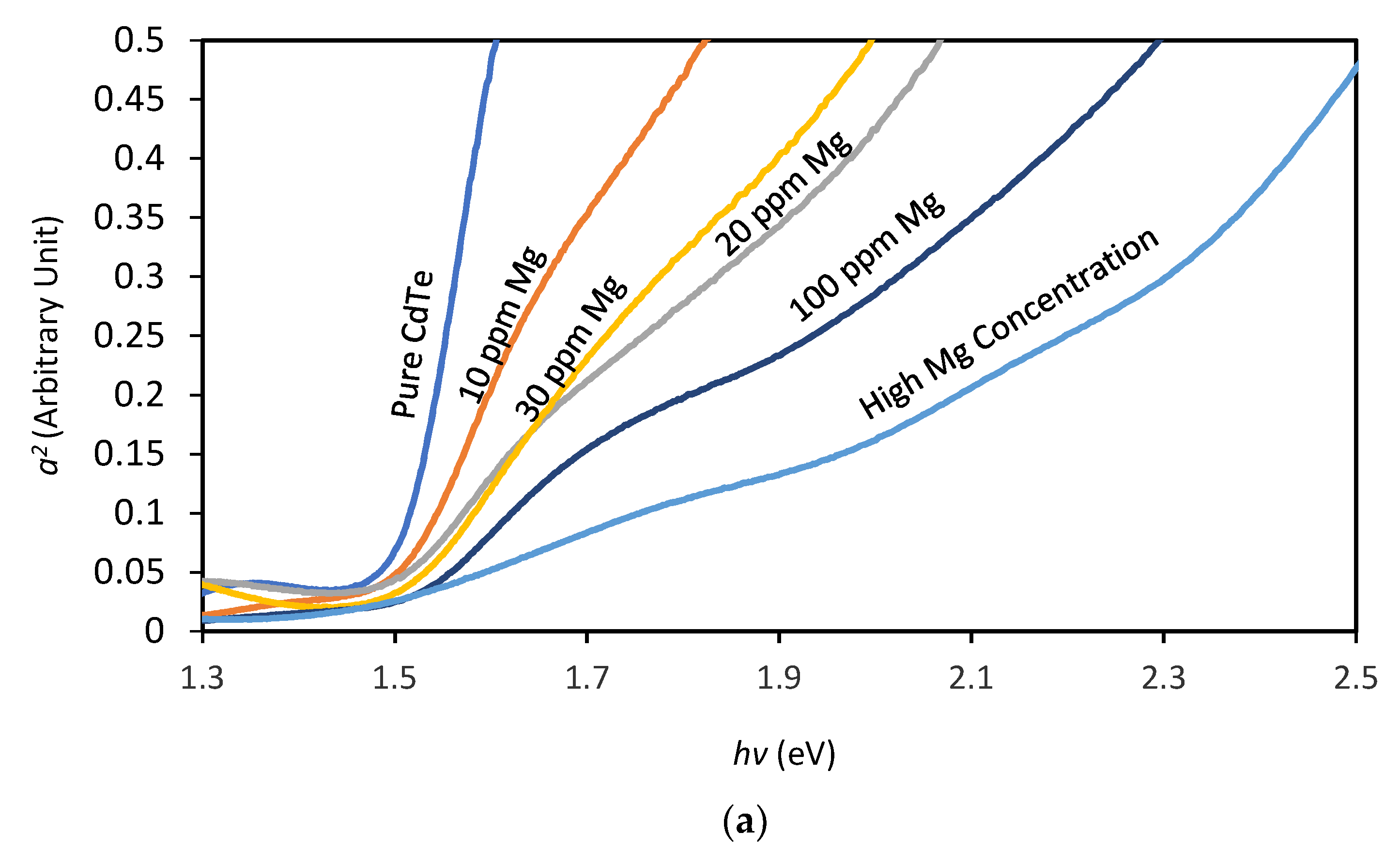
According to
Figure 6a, with the increase of Mg inclusion to the ED bath there appears a gradual disappearance of typical absorption point of CdTe (~1.45 eV) when the growth voltage has been kept constant at 1400 mV. The steepness of the slope at the absorption edge weakens gradually which may indicate a presence of high defect state [
20,
21]. The graph also depicts that at a high (~50%) Mg concentration in the bath, the grown layer does not demonstrate any absorption around the typical CdTe absorption point, therefore indicates a change in the band gap energy. Therefore, the absorption spectra of the layers grown at variable cathodic potentials (Vg) from the bath containing high Mg presence were investigated.
Figure 6b illustrates a higher bandgap of grown layers ranging from ~2.80 to ~2.95 eV. Layers grown at approximately 1400 mV show steeper slopes compared to that of the higher or lower growth voltages.
3.6.2. Photoluminescence (PL) Spectroscopic Study
PL spectra were measured using a Renishaw inVia microRaman/PL system (Renishaw, New Mills, UK). The measurements were performed using a HeNe (632 nm) laser, optics with 1800 diffraction gratin, and a charge-coupled device (CCD) camera as a detector.
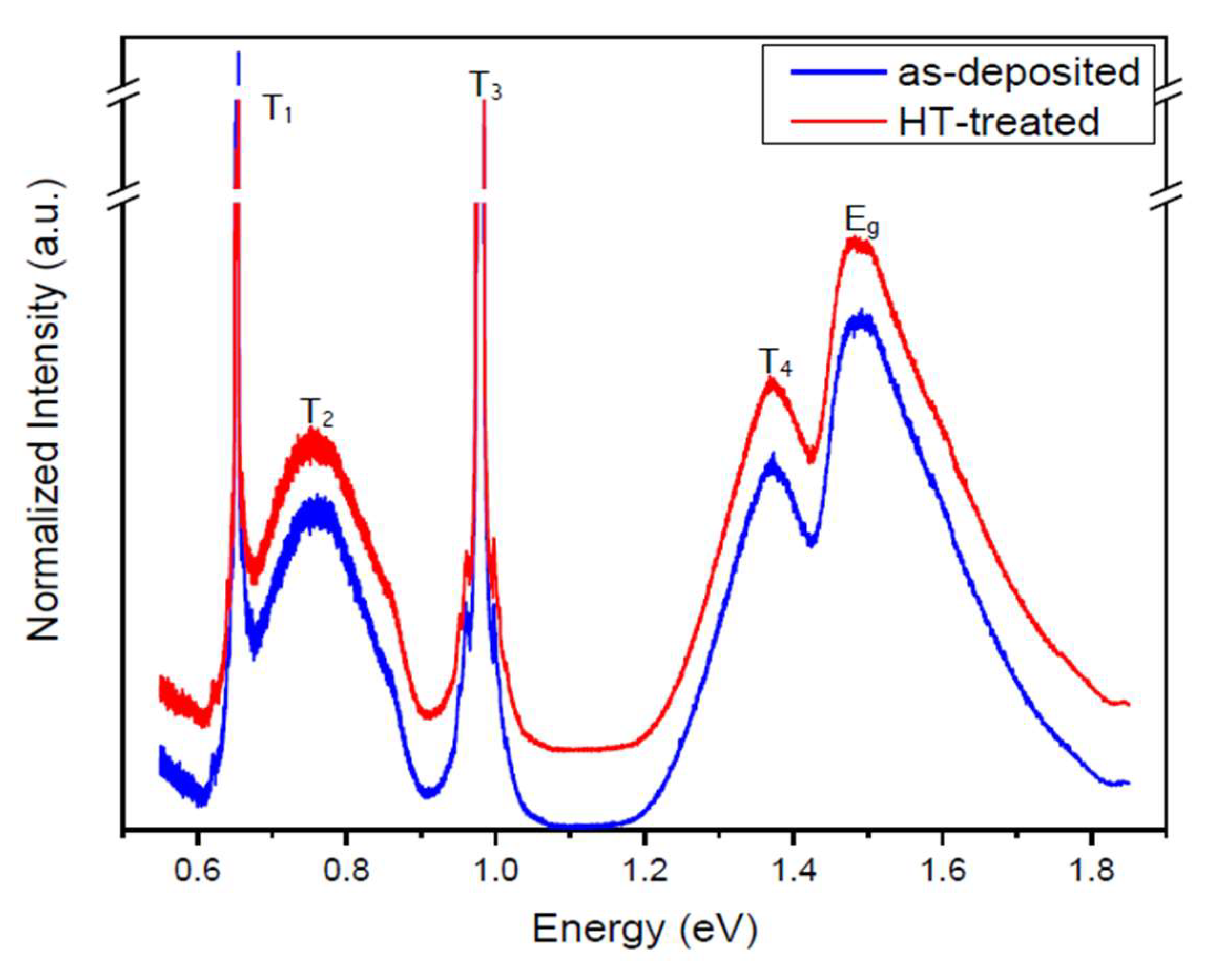
Figure 7 shows the PL spectra obtained for as-deposited and air-annealed CdTe:Mg samples grown with the bath having very high concentration of Mg. Main features of the PL spectra are similar to the PL spectra obtained using the same system and reported in reference [
22]. The defect levels available for CdTe layer at T
1 (~0.66 eV), T
2 (~0.76 eV), T
3 (~0.98 eV), and T
4 (~1.39 eV) are observed for the CdTe:Mg samples, together with E
g at ~1.50 eV. The E
g value observed here corresponds to the CdTe phase. The bandgap for MgTe phase could not be observed because of instrumental limitations restricting higher range (2 to 3 eV) measurements. However, the intensity of T1 and T3 peaks have considerably increased for CdTe:Mg samples when compared to CdTe. Despite considering some instrument induced points at these levels, this shows that Mg in CdTe has introduced large number of defects in the layer. The previously reported PL work [
19] above showed that CdCl
2 treatment reduce these defects. Therefore, when devices are processed with CdCl
2 treatment, superior devices will be produced; any inclusion of Mg at this stage will produce lower efficient devices.
3.7. Scanning Electron Microscopy (SEM) Analysis
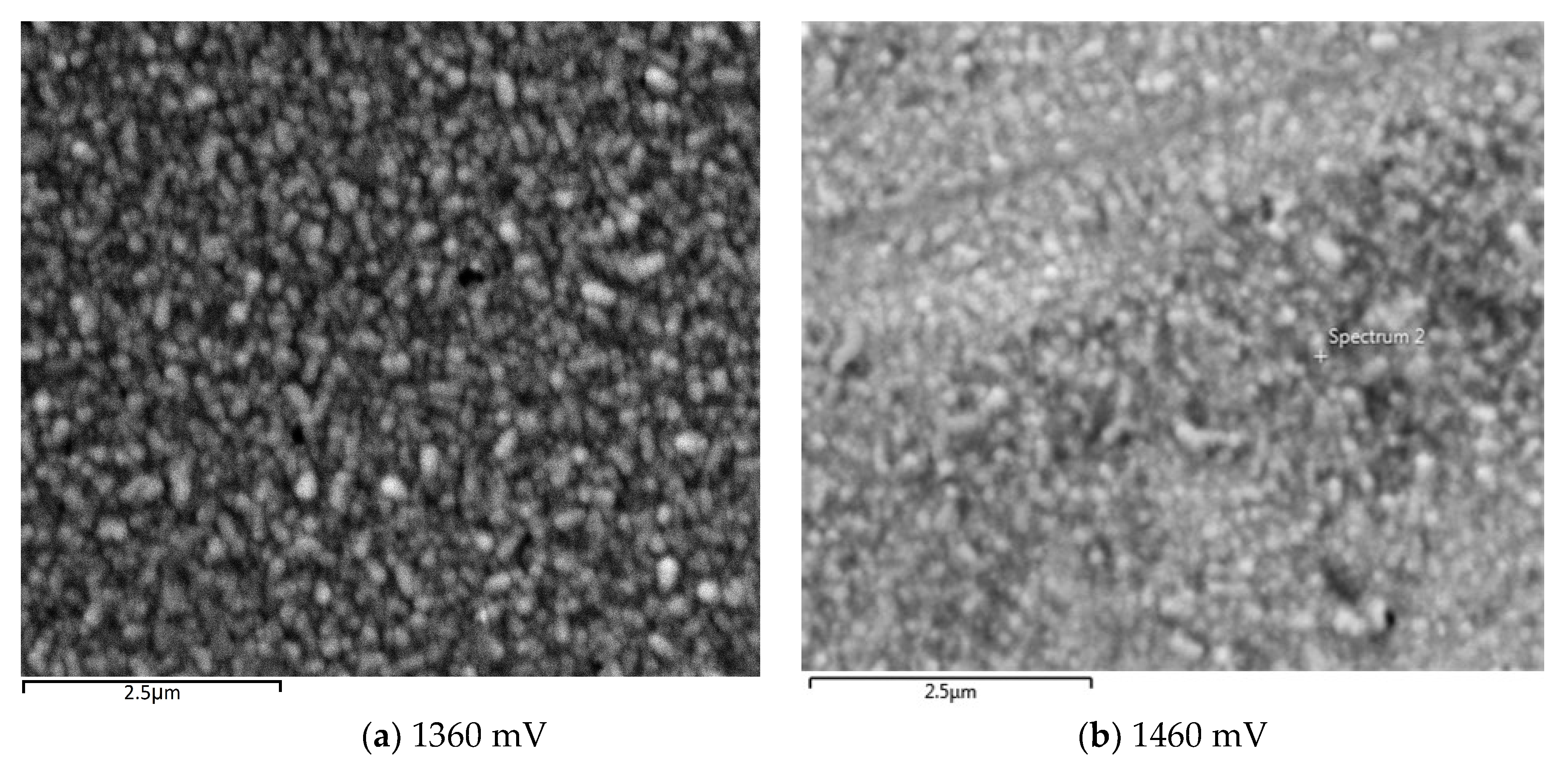
SEM micrographs of the CdTe:Mg films were analysed with a Quanta 650 nano SEM instrument (Thermo Fisher Scientific, Waltham, MA, USA) using 15.0 kV electron beam voltage with magnification of 32,000× for layers grown at different growth potentials. The SEM was carried out to study the morphology and the effects of different Mg inclusion due to the change of cathodic potential for CdTe:Mg films.
Figure 8a–c show SEM images of glass/FTO/CdTe:Mg substrates grown at very high Mg presence in the bath at 1360, 1460 and 1420 mV respectively.
Figure 8a,b show a fairly uniform coverage of glass/FTO that further confirms the amorphous nature of the CdTe:Mg films alongside the XRD outcomes. Though not a clear crystallisation,
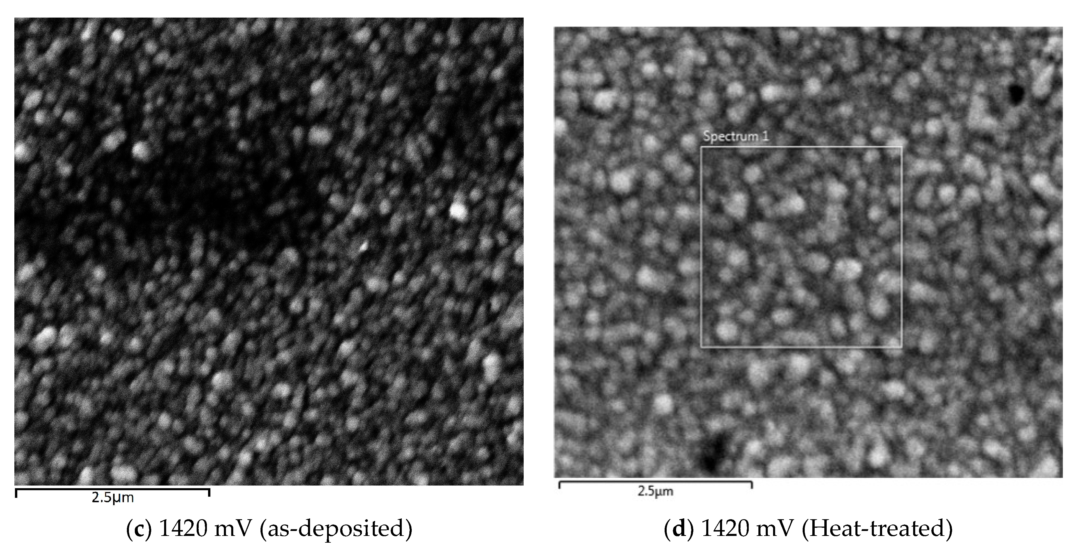
Figure 8c shows a slight agglomeration of small crystallites clustering together when the film is grown at 1420 mV. The layer was then treated with MgCl
2 and annealed for 20 min at 400 °C, which, as per
Figure 8d, contributed to marginally enlarge the clusters but created some pinholes too. This observation is consistent to the previous remarks made in
Section 3.6.1 about layers grown at ~1400 mV having steeper absorption edge slope.
4. Conclusions
The work reported in this paper leads to draw several conclusions. The main conclusions are the conversion of n-type CdTe layers into p-type CdTe:Mg layers as the Mg is incorporated. Also, bandgap widening has taken place from 1.45 eV (CdTe) to 2.85 eV (CdTe:Mg) as expected. However, the structural properties has deteriorated causing the polycrystalline CdTe layer into amorphous CdTe:Mg. PL studies show enhancement of defects within the layers after inclusion of Mg into CdTe. The low crystallinity and high defect levels in CdTe:Mg layers certainly reduce the solar cell performance. However, the wide bandgap p-type nature of CdTe:Mg layers could be useful in development of graded bandgap solar cells with p-type window layers. The work is progressing along this line.
Author Contributions
Conceptualization, A.E.A., A.A.O. and I.M.D.; Methodology, A.E.A. and A.A.O.; Software, A.E.A.; Validation, I.M.D. and J.B.J.; Formal analysis, A.E.A.; Investigation, A.E.A., A.A.O. and J.B.J.; Data curation, A.E.A., A.A.O. and J.B.J.; Supervision, I.M.D.; Visualization, A.E.A.; Writing—original draft, A.E.A.; Writing—review & editing, J.B.J. and I.M.D.; Project administration, I.M.D.; Funding Acquisition, A.E.A.
Funding
This research was funded by the UA Doctoral Training Alliance (DTA), UK and CARA.
Acknowledgments
The authors would like to thank W. Cranton for his advice and M. Leroux for assisting with measurements as the work progressed. The first author also wishes to acknowledge the financial contributions made by the Doctoral Training Alliance (DTA) and CARA for funding the doctoral research, and thanks the University of Liberal Arts Bangladesh (ULAB) for granting study leave to join this research programme.
Conflicts of Interest
The authors declare no conflict of interest.
References
- First Solar. First Solar Achieves Yet Another Cell Conversion Efficiency World Record. Available online: http://investor.firstsolar.com/news-releases/news-release-details/first-solar-achieves-yet-another-cell-conversion-efficiency (accessed on 13 September 2018).
- Peschel, T. CIGS Solar Cells: New European Record of 22% Efficiency. Available online: http://www.sunwindenergy.com/photovoltaics/cigs-solar-cells_-new-european-record-of-22_-efficiency (accessed on 13 September 2018).
- Dharmadasa, I.M.; Samantilleke, A.P.; Chaure, N.B.; Young, J. New ways of developing glass/conducting glass/CdS/CdTe/metal thin-film solar cells based on a new model. Semicond. Sci. Technol. 2002, 17, 1238–1248. [Google Scholar] [CrossRef]
- Ojo, A.A.; Dharmadasa, I.M. 15.3% efficient graded bandgap solar cells fabricated using electroplated CdS and CdTe thin films. Sol. Energy 2016, 136, 10–14. [Google Scholar] [CrossRef]
- Dharmadasa, I.M. Third generation multi-layer tandem solar cells for achieving high conversion efficiencies. Sol. Energy Mater. Sol. Cells 2005, 85, 293–300. [Google Scholar] [CrossRef]
- Dharmadasa, I.M. Advances in Thin-Film Solar Cells, 2nd ed.; Pan Stanford Publishing Pte. Ltd.: Singapore, 2018; ISBN 9789814800129. [Google Scholar]
- Ojo, A.A.; Cranton, W.M.; Dharmadasa, I.M. Next Generation Multilayer Graded Bandgap Solar Cells; Springer International Publishing: Cham, Germany, 2019; ISBN 978-3-319-96666-3. [Google Scholar]
- Echendu, O.K.; Dharmadasa, I.M. Graded-bandgap solar cells using all-electrodeposited ZnS, CdS and CdTe thin-films. Energies 2015, 8, 4416–4435. [Google Scholar] [CrossRef]
- Dharmadasa, I.; Roberts, J.; Hill, G. Third generation multi-layer graded band gap solar cells for achieving high conversion efficiencies—II: Experimental results. Sol. Energy Mater. Sol. Cells 2005, 88, 413–422. [Google Scholar] [CrossRef]
- Waag, A.; Fischer, F.; Litz, T.; Kuhn-Heinrich, B.; Zehnder, U.; Ossau, W.; Spahn, W.; Heinke, H.; Landwehr, G. Wide gap Cd1−xMgxTe: Molecular beam epitaxial growth and characterization. J. Cryst. Growth 1994, 138, 155–160. [Google Scholar] [CrossRef]
- Hartmann, J.M.; Cibert, J.; Kany, F.; Mariette, H.; Charleux, M.; Alleysson, P.; Langer, R.; Feuillet, G. CdTe/MgTe heterostructures: Growth by atomic layer epitaxy and determination of MgTe parameters. J. Appl. Phys. 1996, 80, 6257–6265. [Google Scholar] [CrossRef]
- LeBlanc, E.G.; Edirisooriya, M.; Ogedengbe, O.S.; Noriega, O.C.; Jayathilaka, P.A.R.D.; Rab, S.; Swartz, C.H.; Diercks, D.R.; Burton, G.L.; Gorman, B.P.; et al. Determining and Controlling the Magnesium Composition in CdTe/CdMgTe Heterostructures. J. Electron. Mater. 2017, 46, 5379–5385. [Google Scholar] [CrossRef]
- Dharmadasa, I.M.; Ojo, A.A. Unravelling complex nature of CdS/CdTe based thin film solar cells. J. Mater. Sci. Mater. Electron. 2017, 28, 16598–16617. [Google Scholar] [CrossRef]
- T. F. S. Inc. XPS Reference Table of Elements. Available online: https://xpssimplified.com/periodictable.php (accessed on 19 September 2018).
- Pandey, M.; Jacobsen, K.W. Heats of formation of solids with error estimation: The mBEEF functional with and without fitted reference energies. Phys. Rev. B 2015, 91, 235201. [Google Scholar] [CrossRef]
- Diso, D.G.; Fauzi, F.; Echendu, O.K.; Olusola, O.I.; Dharmadasa, I.M. Optimisation of CdTe electrodeposition voltage for development of CdS/CdTe solar cells of CdS/CdTe solar cells. J. Mater. Sci. Mater. Electron. 2016. [Google Scholar] [CrossRef]
- Greenberg, J.H.; Guskov, V.N.; Lazarev, V.B.; Shebershneva, O.V. Vapor Pressure Scanning of Nonstoichiometry in CdTe. J. Solid State Chem. 1993, 102, 382–389. [Google Scholar] [CrossRef]
- Gulbransen, E.A. The Oxidation and Evaporation of Magnesium at Temperatures from 400 to 500 °C. Trans. Electrochem. Soc. 1945, 87, 589. [Google Scholar] [CrossRef]
- Brookhaven National Laboratory and the US Department of Energy. Nomination of Cadmium Telluride to the National Toxicology Program. Available online: https://ntp.niehs.nih.gov/ntp/htdocs/chem_background/exsumpdf/cdte_508.pdf (accessed on 13 September 2018).
- Dharmadasa, I.; Madugu, M.; Olusola, O.; Echendu, O.; Fauzi, F.; Diso, D.; Weerasinghe, A.; Druffel, T.; Dharmadasa, R.; Lavery, B.; et al. Electroplating of CdTe Thin Films from Cadmium Sulphate Precursor and Comparison of Layers Grown by 3-Electrode and 2-Electrode Systems. Coatings 2017, 7, 17. [Google Scholar] [CrossRef]
- Coulter, J.B.; Birnie, D.P. Assessing Tauc Plot Slope Quantification: ZnO Thin Films as a Model System. Phys. Status Solidi 2018, 255, 1700393. [Google Scholar] [CrossRef]
- Dharmadasa, I.M.; Echendu, O.K.; Fauzi, F.; Abdul-Manaf, N.A.; Salim, H.I.; Druffel, T.; Dharmadasa, R.; Lavery, B. Effects of CdCl2 treatment on deep levels in CdTe and their implications on thin film solar cells: A comprehensive photoluminescence study. J. Mater. Sci. Mater. Electron. 2015, 26, 4571–4583. [Google Scholar] [CrossRef]
© 2018 by the authors. Licensee MDPI, Basel, Switzerland. This article is an open access article distributed under the terms and conditions of the Creative Commons Attribution (CC BY) license (http://creativecommons.org/licenses/by/4.0/).


