Abstract
Nanocrystalline copper oxide thin films were fabricated by reactive DC magnetron sputtering. The structure and optical properties of the films were measured with X-ray diffraction, scanning electron microscopy, and spectrophotometry. Variations of oxygen partial pressure resulted in oxide composition ranging from Cu, Cu-Cu2O, Cu2O-CuO1−x, and CuO. Optical band transitions at 2.06 eV and 2.55 eV were found for Cu2O corresponding to the direct forbidden and direct allowed interband transitions. For CuO an indirect allowed interband transition was found at 1.28 eV. The photocatalytic activity was determined by quantifying the rate constant and quantum yield (destroyed molecules/photons absorbed) under stearic acid degradation. Photocatalytic activity was found to be highest in mixed-phase films with Cu-Cu2O films the highest. Results from post-annealed Cu-Cu2O and CuO films show similar results. We interpret our results as being due to efficient electron-hole charge separation in the heterojunction films. The obtained quantum yields were generally about ten times lower than for comparable dense TiO2 and WO3 binary oxides, which calls for further studies of the spectral dependence of the quantum yield and electron-hole pair life times for oxides with different purity levels.
1. Introduction
Solar light-activated photocatalysis should obviously utilize as large fraction of the solar light as possibly, and there are several ways to improve the catalyst for efficient collection and utilization of the photo-excited charge carriers [1]. Nevertheless, the photo-activity (measured as e.g., quantum efficiency/efficacy or quantum yield [2] for a photocatalytic reaction depends on the band gap of the catalyst, with higher bandgap many times translating to higher efficiency [3], and usually exhibits a complex spectral dependence [4]. At the same time, energetics dictates that the band gap cannot be too small to allow for the chemical reactions to occur. For oxygen and hydroxyl mediated photocatalysis the band gap must be larger enough and the affinity and donor levels must be lower and higher, respectively, than the conduction and valence band edge. For example, to perform the redox chemistry for water cleaning, energetics dictates that the bandgap must be larger than about 2 eV (λ < 600 nm) to produce the OH radicals necessary for pollutant oxidation [5]. Copper and iron oxide-based materials would meet these conditions. The thermodynamic constraints and unfavorable electronic transport in these materials have for long time eluded efficient photocatalysis, but with advent of judicious structure-reactivity analysis and atomic-scale resolved analyses new low-dimensional oxides with beneficial photocatalytic properties have been reported [6,7].
Nanoporous systems for air and water cleaning should have a large internal surface area, which in many cases leads to dimensions that are too small to allow electric fields to build up within the individual building blocks of the material. For the smallest dimensions there is thus no band bending, which has the consequence that diffusion is the dominating mechanism for charge carrier separation. However, by contacting metal, p- and n-type semiconducting nanoparticles the electric field created at their interface, analogous to heterojunctions in solid state electronics, can lead to charge separation due to the charge accumulation/depletion at the interfaces and hence an electric field which facilitates the electron-hole pair separation. These ideas have lead researchers to develop different schemes to fabricate hierarchical photocatalysts [8].
While the photocatalytic activity of single phase Cu2O (cuprous oxide) and CuO (cupric oxide) have been studied by several groups [9,10,11,12,13,14], and been interpreted in terms of nano-morphology, exposed facets and low-coordinated Cu surface atoms, very few studies on mixed CuO-Cu2O or Cu-Cu2O/Cu2O have been reported [15]. Previously, copper oxide heterojunctions have been prepared for photovoltaic [15] and organic dye degradation in aqueous solutions [16,17]. To the best of our knowledge no reports on the photocatalytic of copper oxide heterojunction thin films have been reported. Such films prepared by sputtering methods are readily up-scaled and, importantly, have excellent adhesion with the substrate which is of utmost important in cleantech applications. Herein, we show results for mixed phase, nanostructured copper oxide heterojunction films prepared by dc magnetron sputtering. In particular, we present data for a range of copper oxide compositions and phase mixtures prepared at different oxygen pressures, as well as Cu films calcinated at different temperatures, and carefully assess their photocatalytic efficiency by quantifying the photo-degradation of stearic acid and extract rate constants and quantum yields.
2. Materials and Methods
Thin films of copper and copper oxides of different stoichiometry, ranging from pure metallic Cu, Cu2O to the full oxidized CuO phase were deposited at room temperature by DC magnetron sputtering employing a Balzers UTT 400 unit under conditions that produced nanoporous columnar films [18,19]. The films were deposited onto glass (microscope slides) and the target was a metallic Cu disc (99.995% purity) with 5.8 cm diameter. Starting at a base pressure in the deposition chamber of 10−7 mbar, 50 sccm of Ar (99.998% pure) were introduced in the system. The total pressure in the deposition chamber was then set to 4.0 × 10⁻² mbar. A power of 250 W was applied to the target and voltage and current were allowed to stabilize. Once current and voltage were stable, O2 (99.998% pure) was introduced in the system in fluxes ranging from 0 to 20 sccm, resulting in an increase of the O2 partial pressure (PO2). The deposition time was adjusted for obtaining a thin film thickness of about 200 nm, determined by a Bruker Dektak profilometer (measured at the step between sample and substrate). In order to study the effect of the crystalline structure and phase composition on the photocatalytic activity, some films were annealed in air at 250 °C and 500 °C during 45 min. Table 1 summarizes some deposition parameters (PO2, sample growth rate and discharge current) for CuxOy films deposited at different oxygen flow rates. As expected, PO2 remains equal to 0.0 mbar when the oxygen flow rate is low (0–2 sccm). This is the metallic region [20,21], where the sputtering plasma is able to trap all available oxygen atoms. Samples deposited at these conditions are characterized by larger growing rates and higher discharge current. At higher oxygen flow rates (≥4 sccm) oxygen atoms start reacting with the target, causing a decrease of the sputtering efficiency, and hence a decrease of the growth rate. In this case, the ejected Cu atoms are not able to trap all the available oxygen and hence, from this point, PO2 increases linearly with the oxygen flow rate [20,21]. This is the reactive region, where growth rate and discharge current are smaller and oxides of different stoichiometries are obtained.

Table 1.
Oxygen partial pressure PO2, growth rate, discharge current and grain size (calculated in samples of the indicated thickness by X-ray diffraction, for details see Section 3.1), as a function of the oxygen flow rate. The discharge power was fixed to 250 W, and the argon flux to 50 sccm.
The crystalline structure of the films was studied by grazing incidence X-ray diffraction (GIXRD) employing a Siemens D5000 diffractometer using Cu Kα radiation (λ = 1.5418 Å). The angle of incidence was fixed to 1°. In addition, the microstructure was studied by use of a LEO 1550 FEG Gemini Scanning Electron Microscope (SEM) operating at an acceleration voltage of 5 kV.
The optical absorption, α, in the films was determined from the measured transmittance (T) and reflectance (R) of the films using a Perkin-Elmer Lambda 900, equipped with a calibrated integrating sphere [22,23]. The photocatalytic activity of the films was determined by in situ Fourier-Transform Infrared Spectroscopy (FTIR) using a Bruker IFS66v/S spectrophotometer equipped with a liquid-nitrogen cooled HgCdTe detector employing 4 cm−1 spectral resolution and 30 s scan time/30 s dwell time between spectral acquisition. A home-built specular reflection cell was used in the in situ FTIR measurements. For the evaluation of the photocatalytic activity of the CuxOy thin films, a solution 8 mM of stearic acid (StA) in methanol was spin-coated onto the film surface. The decrease of the absorption peak in the infrared, corresponding to ν(C-H) vibration from StA (located between 3000 and 2800 cm−1) was measured by in situ FTIR measurements under illumination by a Hg lamp operated at 200 W (Oriel Instruments) filtered with a 54 mm long water filter (de ionized water, 18.3 MΩ) and a 0.5 neutral density filter to reduce the photon power. The Hg lamp presents all its main emission peaks above 2.0 eV (4.9, 4.1, 3.9, 3.7, 2.6, 3.0, 2.8, 2.3 and 2.1 eV), i.e., the photons emitted by the lamp have enough energy to excite electrons from the valence band to the conduction band in both CuO (band gap of ~1.1 eV) and Cu2O (bandgap of ~2 eV) [24]. The photon power was 42 mW cm−2 at the sample position, as measured by a thermopile detector.
3. Results and Discussion
3.1. Deposition of CuxOy by Magnetron Sputtering
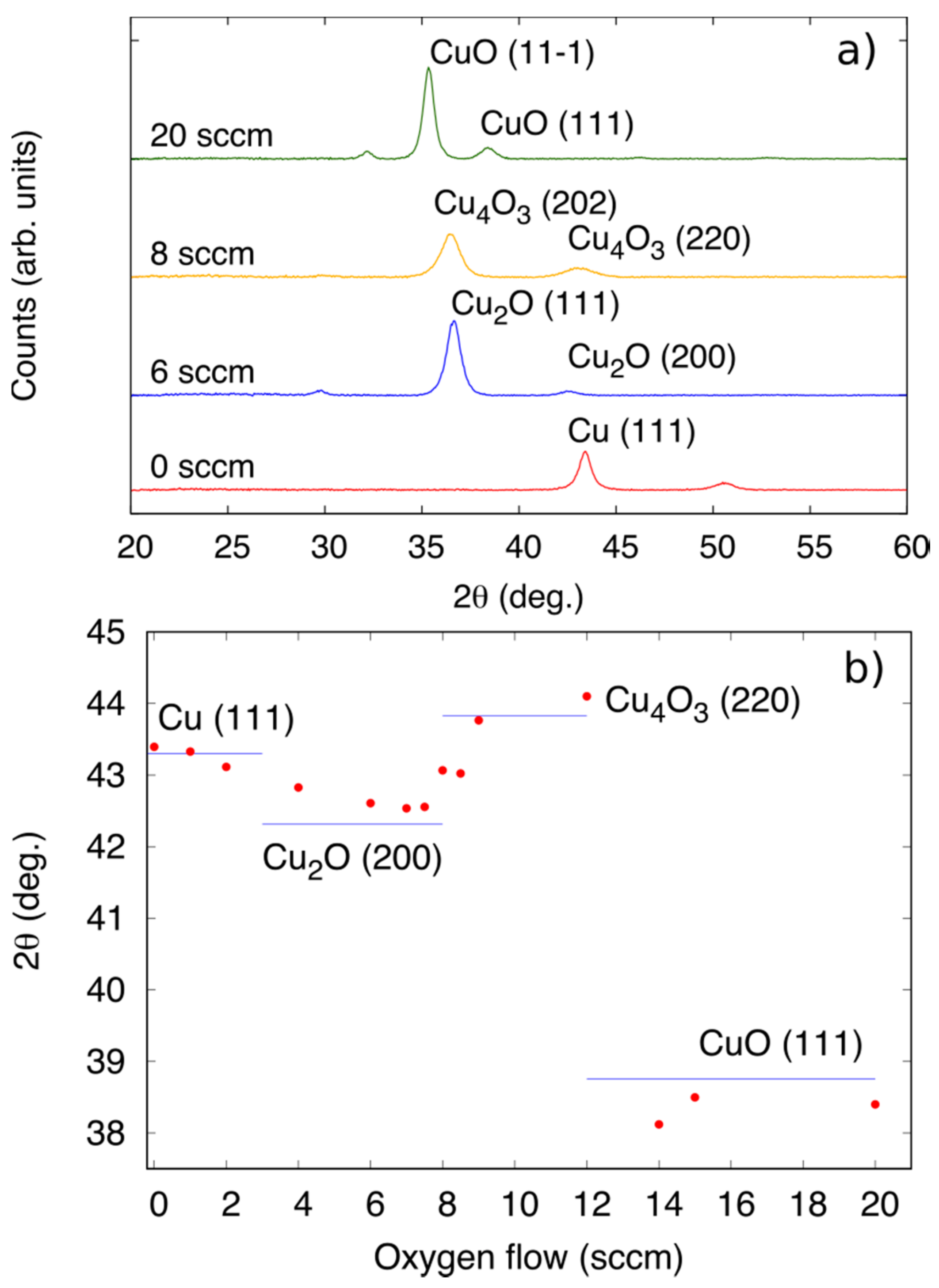
Fine control of the stoichiometry of CuxOy films obtained by magnetron sputtering can be achieved by adjusting the oxygen flow (and hence oxygen partial pressure) during the deposition process (Table 1). Figure 1a depicts the X-ray diffractograms corresponding to different films deposited at O2 fluxes of 0, 6, 8 and 20 sccm. As expected, with no oxygen flow only a metallic Cu phase is observed in the diffractogram. At 6 sccm, however, only the characteristic diffraction peaks corresponding to the Cu2O phase are observed. Higher oxygen fluxes result in the fully oxidized CuO phase. In between those two phases, a range of intermediate stoichiometries are obtained, including Cu4O3 [25,26], which is an intermediate state between CuO and CuO2. Assignments of the diffraction peaks were done using the Joint Committee on Powder Diffraction Standards (JCPDS) cards 00-004-0836 (metallic Cu, cubic) 04-007-9767 (Cu2O cubic), 04-007-2184 (Cu4O3, tetragonal) and 00-048-1548 for the fully oxidized CuO phase (monoclinic). For analysis of the variation of the stoichiometry of the films as a function of the oxygen flux the region between 35° < 2θ < 48° degrees was studied, rather than the high intensity reflections, i.e., <111>, <202> and <11-1> in Cu2O, Cu4O3 and CuO, respectively. This is because the angle of the reflection peak between 38° and 45° first decreases as the material evolves from metallic Cu to a Cu2O stoichiometry (<200> peak), and then increases as the samples are close to the Cu4O3 stoichiometry (<220> peak), decreasing again as it attains CuO stoichiometry (<111> peak). In contrast, the high intensity reflection angles appear at progressively smaller angles as the oxidation state of Cu increases (see Figure 1).
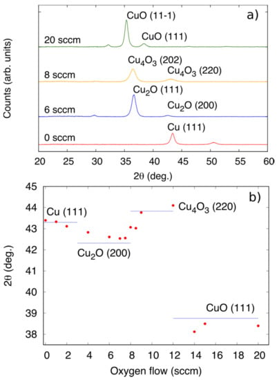
Figure 1.
(a) X-ray diffraction patterns corresponding to the as-deposited thin films synthesized at different oxygen flow. (b) Position of the diffraction peak observed at 35° < 2θ < 48° as a function of the oxygen flow used during deposition.
Thus, monitoring the diffraction peaks in the 38° < 2θ < 45° region as a function of the Cu film oxidation (i.e., oxygen partial pressure, in the synthesis), the Cu2O stoichiometry can therefore be associated with a minimum of reflection angle due the <200> reflection. Similarly, an abrupt decrease of the diffraction angle is expected as the <220> reflection due to the Cu4O3 phase, transforms into the fully oxidized CuO phase. Following this reasoning, Figure 1b shows the position of the diffraction peak (38° < 2θ < 45°) as a function of oxygen flux. Thus, at flow rates between 1 to 6 sccm films are composed of a Cu2O phase, rich in defects as evidenced by the smaller interplanar spacing (corresponding to the <200> reflection) compared to stoichiometric Cu2O (Figure 1). We attribute this smaller interplanar distance to either oxygen vacancies or Cu metal additions in the lattice. At around 6 sccm, the Cu2O phase is formed, and is associated with a local minimum in 2θ. Higher oxygen fluxes, between 6 and 12 sccm, lead again to the increase of the angle of the diffraction peak between 38° < 2θ < 45°, and correspond to CuO1−x stoichiometry, with x < 1, notably we expect that Cu4O3 is formed in this region [25,26]. The abrupt decrease of angle of the diffraction peak observed at high oxygen fluxes (>12 sccm) shows that films with CuO stoichiometry are formed under these sputtering conditions. A similar variation of the diffraction peak angles for the different Cu oxide phases between 38° < 2θ < 45° has also been reported by Meyer et al. [26].
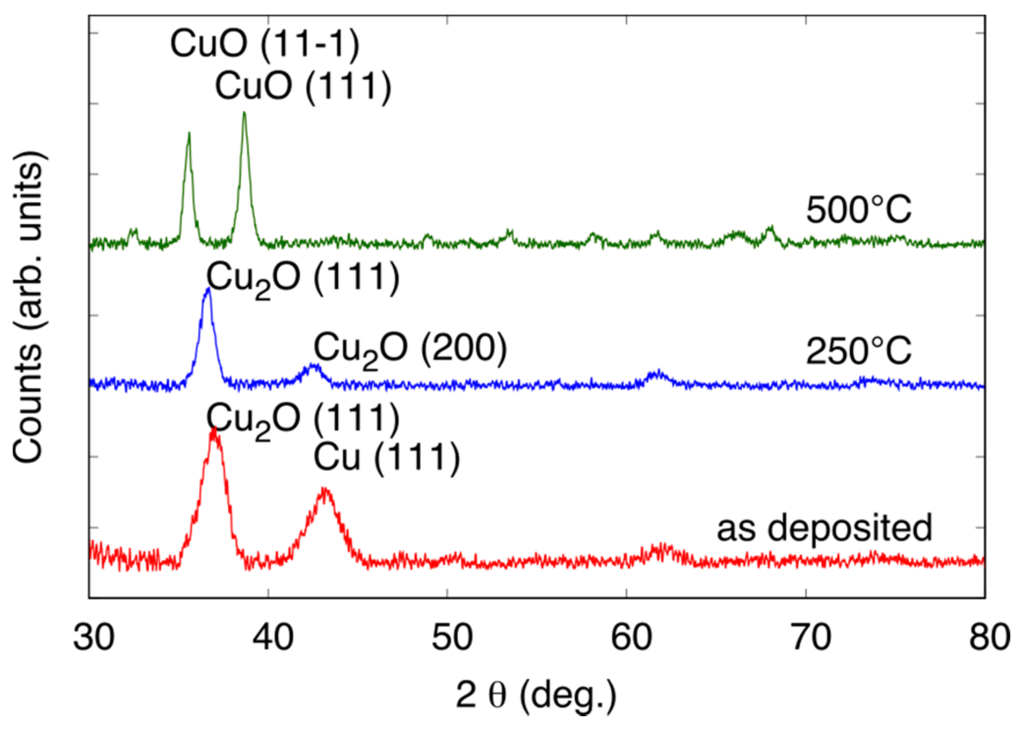
The stoichiometry of the films was also varied after deposition by using different annealing processes in air, as shown in Figure 2. In particular, samples deposited at low oxygen flow (2 sccm) which present XRD peaks corresponding to both metallic Cu and Cu2O (Figure 2 lowest curve), although not fully oxidized, evolve towards Cu2O stoichiometry after an annealing process at 250 °C in air during 45 min (Figure 2 intermediate curve). If the annealing is carried out at 500 °C instead, the X-ray diffraction patterns show only the CuO characteristic peaks (Figure 2 top curve).
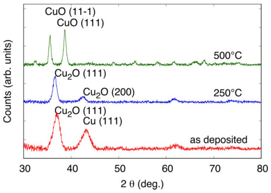
Figure 2.
X-ray diffractograms corresponding to samples deposited 2 sccm oxygen flow, as-deposited and after 250 °C or 500 °C annealing in air.
SEM micrographs are presented in Figure 3 for films deposited at oxygen flow rate of 2 sccm [panel (a)], 6 sccm [panel (b)], and 20 sccm [panel (c)]. Figure 3 shows how the increase in oxygen flow rate results in growth of a nanoporous layer which we attribute to a columnar growth of copper oxide [18]. The protrusion visible in SEM are slightly larger than the grain sizes deduced from XRD, and are thus composed of polycrystalline grains. By using Scherrer’s formula and the XRD data presented in Figure 1a, the mean grain size of the films was estimated to be 5.36, 9.74 and 12.95 nm, respectively, for samples shown in Figure 3a–c, (calculated from highest intensity peak in the XRD pattern and assuming a shape factor of 0.9 in Scherrer’s equation). Grain sizes corresponding to other films are presented in Table 1. The largest grain size (around 10 nm) was achieved close to stoichiometric conditions, namely Cu metallic (0 sccm), Cu2O (6.0–7.5 sccm) and CuO (20.0 sccm). As expected, intermediate conditions resulted in smaller grain sizes due to the presence of lattice defects. Regarding the effect of the annealing of the size and morphology of the films, Figure 3d corresponds to a sample deposited at 2 sccm which was subsequently annealed in air at 500 °C during 45 min. The grain sizes, calculated from the XRD data presented in Figure 2, increased from 5.36 to 9.27 and 16.10, respectively, for as-deposited films annealed to the 250 °C and 500 °C. Before annealing, the morphology of the samples deposited at 2 sccm (Figure 3a) exhibited protrusions and irregularities, which is attributed to the Cu metallic phase, since they disappear after annealing (Figure 3d), or when the oxygen flow rate is increased (Figure 3b,c).
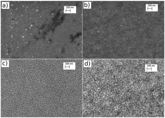
Figure 3.
Micrographs (5 KV acceleration voltage ×50 K magnification) for as deposited samples deposited at (a) 2 sccm, (b) 6 sccm, (c) and 20 sccm (c). A sample deposited at 2 sccm and annealed at 500 °C during 45 min is shown in (d).
3.2. Optical Properties
The absorption coefficient, α, was determined using the measured reflectance (R) and transmittance (T) curves following the relation [22]:
where d is the film thickness. The energy of the optical band gap was determined by Tauc analysis by plotting (αE)a vs. E, where E is the energy of the incident photon, and a an exponent that depends on the characteristics of the transition. In particular, a = 2, 2/3 and 1/2, for a direct allowed, direct forbidden or indirect allowed band gap transitions, respectively [27]. The energy of the band gap transition was determined by the intersection between the extrapolated linear part of the absorption edge and the abscissa axis.
Cu2O is known to exhibit both a direct forbidden and a direct allowed transition, with the latter located approximately +0.45 eV above the direct forbidden transition [24]. According to Figure 1b films deposited at 6 sccm are likely to present Cu2O stoichiometry. In Figure 4a,b show plots of (αE)2/3 and (αE)2 vs. E. It is seen that films deposited at 6 sccm O2 flow are well described by an absorption edge characterized by a direct forbidden transition at 2.06 eV followed by a direct allowed transition at 2.55 eV, in excellent agreement with previous reports for Cu2O [24]. Regarding CuO, it is not well stablished in the literature whether CuO presents a direct or indirect transition [24]. In our case, the CuO samples obtained at 20 sccm exhibit a clear indirect allowed transition located at 1.28 eV, Figure 4c, which is in good agreement with the value of 1.24 eV reported by Wang et al. [24] for CuO.

Figure 4.
Tauc plots showing (a) (αE)2/3 vs. phonon energy, E, and (b) (αE)2 vs. E for a nanocrystalline film deposited at 6 sccm O2 (corresponding to Cu2O stoichiometry). (c) (αE)1/2 vs. E plot for a film deposited at 20 sccm O2 (corresponding to CuO stoichiometry).
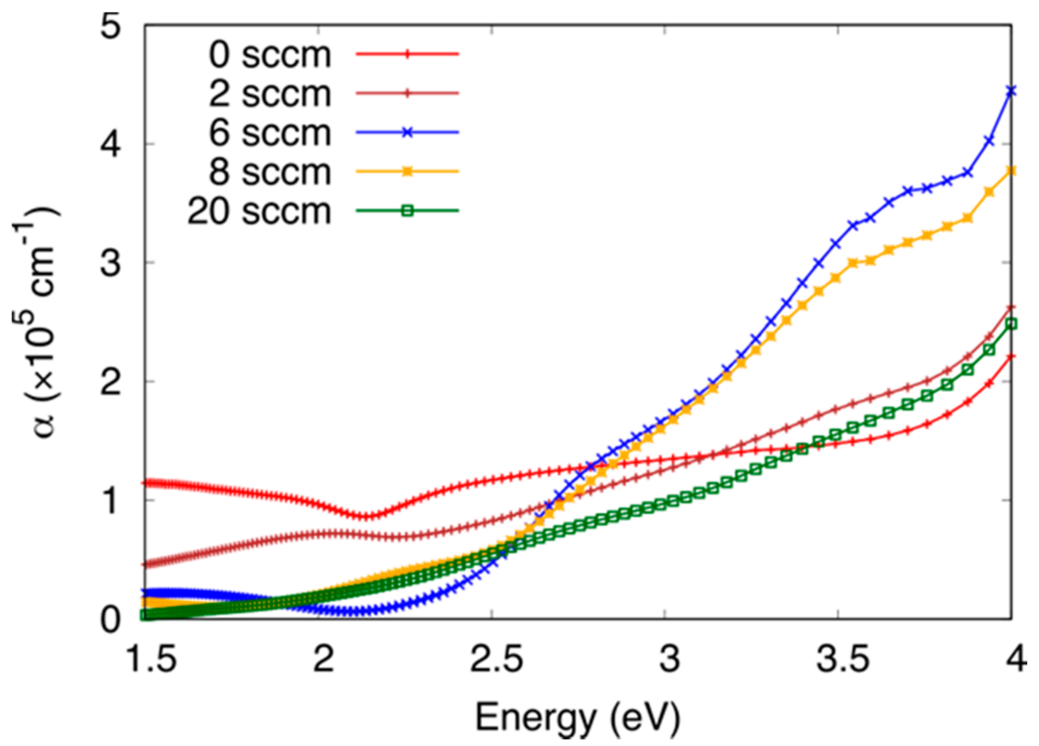
It is now possible to proceed to the analysis of samples deposited at intermediate oxygen fluxes. For this purpose, it is possible to assume that samples deposited at 6 sccm and 20 sccm O2 behave in accordance with the Cu2O and CuO phases, respectively, while samples deposited at 0 sccm are metallic Cu. On this basis, the absorption coefficient, α, has been plotted as a function of E in Figure 5 for films deposited at 0.0 sccm (metallic Cu), 2.0 sccm, 6 sccm (Cu2O), 8.0 sccm and 20.0 sccm (CuO). The thickness of each film corresponds to the data presented in Table 1, except in the case of metallic Cu samples; in this case the optical properties presented in Figure 5 correspond to a ~60 nm-thick Cu film which exhibit some optical transparency. As expected, metallic Cu films show a slight minimum of the absorption coefficient curve at 2.10 eV (orange color) due to well-known interband transitions [28] responsible for the characteristic visual appearance of metallic Cu. The absorption coefficient corresponding to samples deposited at low oxygen flows (2 sccm) still exhibit metallic features such as big optical absorption in the visible region. On the other hand, samples deposited at 8.0 sccm O2 (Cu4O3) can be understood optically as mixtures of CuO (below 2.5 eV, α presents the same features as α measured in samples deposited at 20 sccm O2) and Cu2O (above 2.5 eV, α presents the same trend as α corresponding to films deposited at 6 sccm O2). Thus the mixed phase oxide films can be described by a superposition of interband transitions from the constituent oxide phases, and support the existence of separate domains of crystalline phases.
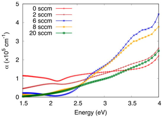
Figure 5.
Absorption coefficient, α, plotted vs. the energy of the incident photon for different samples deposited at different oxygen fluxes.
3.3. Photodegradation of Stearic Acid
3.3.1. Effect of the Oxygen Flux
The integrated absorbance of the ν(CH) stretching bands in StA (CH3(CH2)16COOH) was measured as a function of illumination time to quantify the photo-degradation efficiency. Figure 6 shows in situ FTIR reflection spectra acquired at different irradiation times of StA coated CuxOy films prepared at 2, 12 and 20 sccm oxygen flow rates, corresponding to films with mixed Cu/Cu2O, mixed Cu2O/CuO, and predominantly CuO phases, respectively. In Figure 6, the asymmetric, νas(CH), and symmetric, νs(CH), stretching modes of the CH2 group lie at 2914 and 2846 cm–1, respectively, and the in-plane stretch of the CH3 group lies at 2952 cm–1 [29]. We note that for an organic layer deposited on a dielectric with refractive index of the order n ~ 2.3 (value for Cu2O at 3 μm [30]) that is measured in air, the reflection bands correspond to IR absorption by StA and show up as emission bands [31].

Figure 6.
In-situ FTIR reflection spectra (baseline corrected) acquired after 0, 60 and 120 min of irradiation time; the spectra correspond to samples deposited at different oxygen fluxes: 2 sccm (a), 12 sccm (b) and 20 sccm (c) coated with StA. The figure show the asymmetric νas(CH), and symmetric, νs(CH), stretching modes of the CH2 group present in StA.
Photodegradation of stearic acid onto thin films is known to follow first-order kinetics [29,32], i.e., the integrated peak area (A) depends on time as follows:
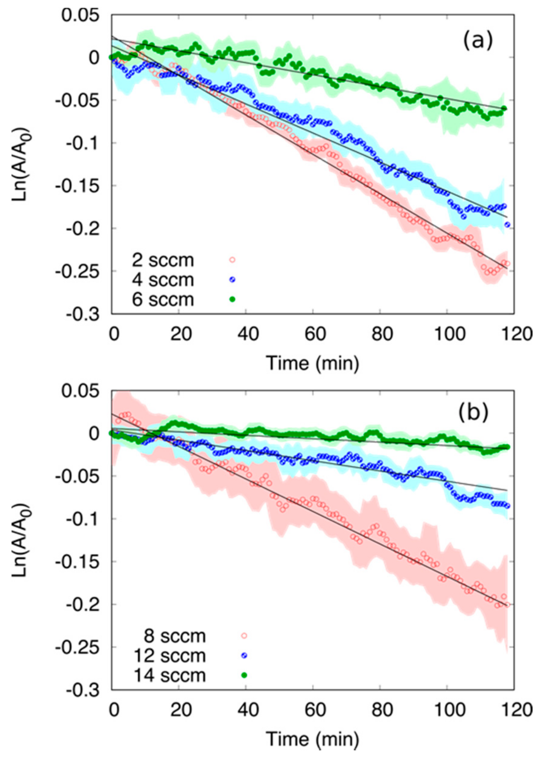
where A0 is the initial integrated peak area (t = 0) and at time t respectively and k is photodegradation rate. Figure 7 shows ln(A/A0) vs. t for samples deposited at low/medium oxygen flow rates (2, 4 and 6 sccm) [panel (a)] and medium high (8, 12 and 14 sccm) [panel (b)]. Results depicted in Figure 7 have been obtained by the average over 5 measurements. The shadow of each curve signifies the error, calculated as the average ± the standard deviation for each point. Irrespective of the oxygen flow rate used during deposition, the curves presented in Figure 7 follow a linear trend throughout the irradiation time. The photodegradation rate, k, was obtained as the value of the slope of the linear fit (solid black lines presented in Figure 7) for each case. Figure 8 shows the initial photodegradation rate, , calculated for films deposited at different oxygen flow rates; is defined as the derivative of Equation (2) evaluated at t = 0, i.e.,
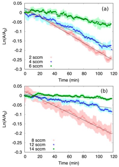
Figure 7.
Plot of the logarithm of the ratio between the integrated area, A, normalized to the initial area, A0 (t = 0 min) vs. irradiation time for samples deposited al low/medium oxygen flow rates (a) and medium/high rates (b). A linear fit to the data points, shown by a solid black line, is shown in each case.
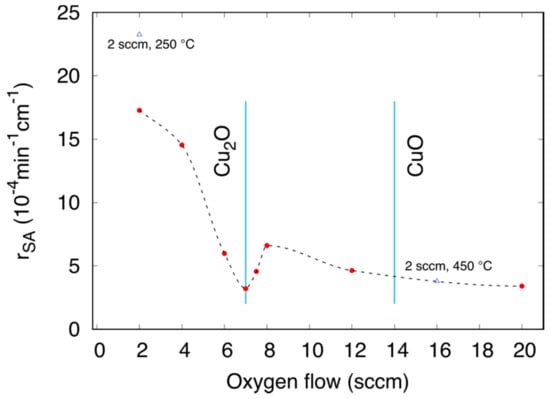
Figure 8.
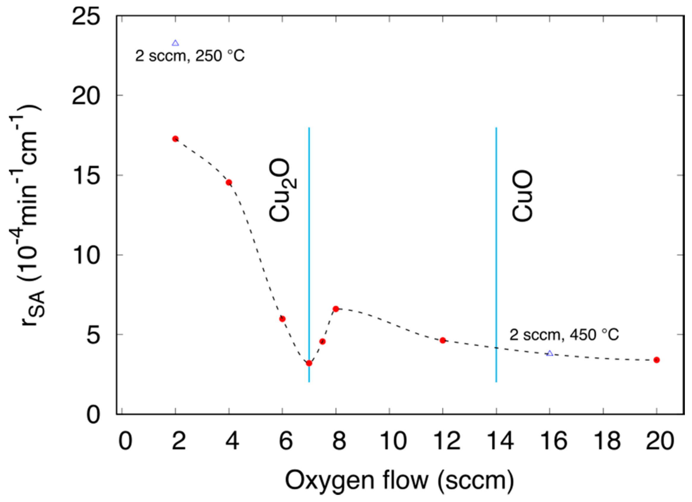
Stearic acid photodegradation rate at t = 0, , for samples deposited at oxygen flow rates ranging from 2 to 20 sccm (solid red circles) using Equation (3). Corresponding data for films prepared at 2 sccm post-annealed at 250 °C (exhibiting Cu2O structure) and 450 °C (exhibiting CuO structure) are shown for comparison (blue open triangles).
It is evident that the highest photodegradation rate is achieved in films deposited a low oxygen flow rate. As the oxygen flow rate is increased from 2 sccm, the obtained films decrease their StA photodegradation rate, reaching a local minimum around 7 sccm (corresponding to the Cu2O phase). Once the oxygen flow rate is increased above 7 sccm the photodegradation rate increases again. However, for oxygen flux rate equal and above 12 sccm, the photodegradation rate drops again, as the samples approach the CuO stoichiometry. Similar measurements on metallic Cu resulted in very poor StA adsorption and no discernable photo-activity could be observed.
According to Figure 8 the photodegradation rate is seen to depend critically on the deposition conditions and a clear correlation between Cu oxide structure (Figure 1b) and photocatalytic activity (Figure 8) is observed. Samples obtained at low oxygen flow rates (2, 4 sccm), which correspond to oxygen deficient Cu2O mixed in metallic Cu, exhibit a higher than more stoichiometric Cu2O films (6, 7 and 8 sccm). Intermediate conditions, corresponding to mixes between CuO, Cu3O4 and Cu2O resulted again in an increase of the photocatalytic activity. The photocatalytic activity decreases however drastically for the films corresponding to CuO stoichiometry (oxygen fluxes > 12 sccm).
Previously, it has been reported that pn-type junction Cu2O-CuO films can be fabricated based on n-type Cu2O that exhibits oxygen vacancies or additional Cu atoms, and p-type CuO films. Such pn-junctions are effective for electron-hole pair charge separation and show an enhanced photoconductivity [15]. Li et al. [16] and Jiang et al. [17] have reported an enhanced photodegradation of dyes in aqueous solutions and attributed their observations to charge separation at the Cu2O/CuO interfaces as being due to their different valance and conduction band positions (with the Cu2O edges located at lower energy with respect to vacuum compared to CuO). Our results clearly show that the mixed metallic Cu-Cu2O is the most active film; much more effective compared with mixed Cu2O-Cu3O4/CuO films. We suggest that the high activity of the Cu-Cu2O films is due an enhanced charge separation due to the dual action of the p-type Cu2O for hole oxidation and the metallic Cu for electron scavenging. An enhanced photo-activity of Cu2O films with Cu deposits [15], and CuO/Cu2O/Cu [16] have also been reported that qualitatively support this interpretation. Similarly, the local maximum of the photocatalytic reaction rate at about 8 sccm may be attributed to the existence of creation of internal electric fields across oxide heterojunction phases that may enhance charge separation.
To further quantify the observed StA photodegradation and compare those with the photo-activity of other binary oxides, the quantum yield, Φ, was calculated according to [33]:
where N1A.U. is the number of StA molecules per cm2 per integrated reflectance unit and F(λ) is the photon flux of the lamp at wavelength, λ, α is the absorption coefficient, and d is the film thickness. For simplicity, we assume N1A.U. = 9.7 × 10¹⁵ molecules/cm2, which is the value usually accepted for StA per absorbance unit for StA on TiO2 [34]. F(λ) has been calculated by the irradiance curve of the Hg lamp (Oriel data sheet) and the illumination power measured by the thermopile in the sample position (42 mW/cm2). In particular, the lamp to emits 9.61 × 10¹⁶ photons cm−2 s−1 in the wavelength range between 250 and 800 nm. Equation (4) represents a lower limit of the quantum yield, since it assumes that all the electrons excited by the absorbed photons reach the surface, but is higher than the so called formal quantum yield [34], which normalize the chemical rate to the number of incident photons. However, the quantum yield is the preferred quantity since it removes differences due scattering which may be significant for nano- and microparticulate systems. Since we have quantified the absorption coefficient we therefore here pursue to calculate the quantum yield. Table 2 presents Φ calculated according to Equation (4) for samples deposited at different oxygen flow rates. In addition, the photodegradation rate, k, the absorbed photons per unit of area and time, given by the denominator in Equation (4), and the initial amount of StA molecules per unit of area (calculated by the product A0·N1A.U.) are also presented in Table 2 for each case. The calculated quantum yield vs. oxygen flow follows the rate constant in Figure 8. In particular, Φ is higher for the Cu + Cu2O films (2, 4 sccm), decreasing as stoichiometric Cu2O is approached (7 sccm). Φ increases again in samples composed of Cu2O + CuO (7.5 and 8 sccm), while the films consisting of CuO stoichiometry exhibit the lowest Φ values. In general, Φ for the mixed copper oxide phases is much lower than reported data for nano-particulate TiO2 (about 1000 times lower than P25 with reasonable estimates of the photon absorption [34]), which mainly is due to the much higher collection efficiency of the photo-excited electrons at the surfaces of small nanoparticles, where the minority charge diffusion length is larger than particle dimension. A more relevant comparison is that for dense films prepared by sputtering or chemical vapor deposition (CVD). We find that our calculated Φ is about 10 times smaller than for sputtered WO3 thin film [33], and about 10 times lower than for a commercial ActiveTM TiO2 thin films prepared by CVD. The conduction and valance band edges, respectively, for Cu2O are however favorable for O2 reduction and hydroxyl oxidation (see e.g., [16] and references therein). It is however clear that the crystallinity of the phases are crucial as can be seen in Table 2 for the post-annealed and sputtered Cu-Cu2O films, with the former exhibiting more pronounced and larger crystalline grains. Further studies of the spectral dependence of Φ are required to shed light on the dependence of the type of interband transition and the electron-hole pair life time.

Table 2.
Photodegradation rate, initial stearic acid coverage (molecules per cm2), absorbed photons and quantum yield, for samples deposited at different oxygen flux rates. Data for samples deposited at 2 sccm and annealed at 250 or 450 °C samples are also included.
3.3.2. Effect of the Annealing
According to the results presented in Section 3.3.1, the photodegradation rate of StA decreases when the films approach Cu2O or CuO stoichiometries. Annealing processes are usually performed for achieving stoichiometric samples [35] and hence, is difficult to employ for making heterojunction oxide films since thermodynamics readily drive the oxide to CuO. By annealing a sputtered film prepared at 2 sccm to 250 °C we find however that it is possible to form Cu-Cu2O films with well-developed crystalline phases. We were not able to produce Cu2O-CuO heterojunctions by post-annealing, as previously reported for annealing of Cu nets, where effective CuO/Cu2O/Cu hierarchical structures were formed [16]. This points to the importance of controlling the substrate morphology to enable growth sites for CuO from Cu2O, while maintaining a Cu phase for continuous Cu2O formation.
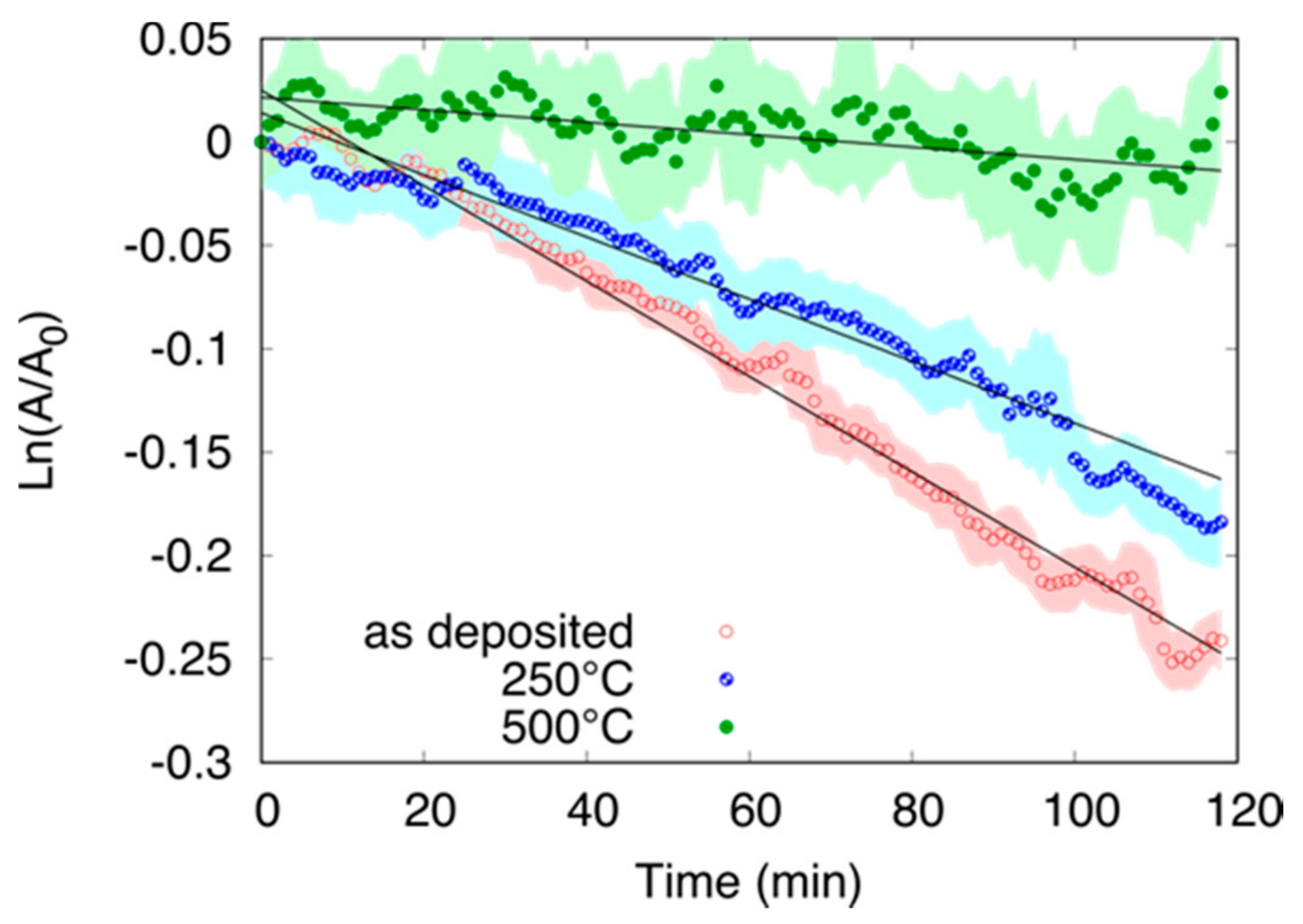
Figure 9 shows ln(A/A0) vs. time plotted for samples deposited at 2 sccm oxygen flow rate, as deposited and annealed in air at 250 °C and 500 °C during 45 min. X-ray diffraction patterns corresponding to these samples were presented in Figure 2. As in the case of Figure 7, the data presented in Figure 9 have been obtained by a 5-point average, where the shadow of each curve signifies the error, calculated as the average ± the standard deviation for each point. Similarly, k was obtained as the absolute value of the slope of the linear fit (solid black lines presented in Figure 9) for each case. For the as-deposited sample (consisting on a mix between Cu and Cu2O phases), k = 2.30 × 10⁻³ min−1. As expected, k decreases slightly after 250 °C annealing, when the film approaches Cu2O stoichiometry (k = 1.50 × 10⁻³ min−1), dropping abruptly after 500 °C annealing (k = 0.30 × 10⁻³ min−1) approach the same degradation rate as the CuO films prepared at high O2 flow (see Table 2). The rate constants and quantum yield for the post-annealed films are shown in Figure 8 and Table 2. We see that the post-annealed films show the same behavior as the sputtered films with the Cu-Cu2O film exhibiting the highest rate. The rate and quantum yield for the post-annealed Cu-Cu2O heterojunction film are the highest of all measured films, and is attributed to the well-developed Cu and Cu2O phases and grain boundaries formed upon annealing [16].
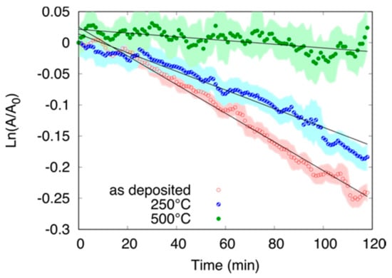
Figure 9.
Stearic acid photodegradation rate at t = 0, , for samples deposited at oxygen flow rates ranging from 2 to 20 sccm (solid red circles). Corresponding data for films prepared at 2 sccm post-annealed at 250 °C (exhibiting Cu2O structure) and 450 °C (exhibiting CuO structure) are shown for comparison (blue open triangles).
4. Conclusions
Copper oxide thin films with different phase compositions have been fabricated by reactive dc magnetron sputtering. We find that by controlling the oxygen partial pressure while keeping the total pressure constant, nanostructured films exhibiting metallic Cu-Cu2O, Cu2O-CuO1−x, and CuO can be made. The films are characterized by small clusters of the order 100 nm composed of crystalline oxide grains. The optical properties of the films reveal that the Cu2O phase is associated with a direct forbidden and direct allowed interband transitions at 2.06 eV and 2.55 eV, respectively, while CuO possesses an indirect allowed interband transition at 1.28 eV. The mixed phase oxides could be well described by superpositions of interband transitions from the constituent oxide phases, supporting the existence of separate domains of crystalline phases. Careful analysis of the photodegradation rate of stearic acid spin coated on the surfaces of the films revealed that the mixed phase Cu-Cu2O and Cu2O-CuO1−x films were more active than the pure phase oxides, with the Cu-Cu2O heterojunction film being the most active. We remark that heterojunction films are more difficult to fabricate in a controlled manner by post-annealing procedures in air due to thermodynamic driving force to form single phase oxide, with CuO being the most stable. The results support the idea that electron-hole separation at the interfaces between metal and oxide grains occurs and is translated to a higher photodegradation rate. The results that the Cu-Cu2O film prepared by post-annealing has the highest photo-activity suggests that formation of well-developed crystalline grain boundaries between the Cu and Cu2O phases is beneficial for a high photodegradation rate, and further support a mechanism where charge separation at the Cu-Cu2O drives the reaction. In general, the calculated quantum yields are however about ten times lower than for comparable n-type binary oxides (TiO2 and WO3) and points to different rate determining step(s) for p-type copper oxides.
Author Contributions
Conceptualization of the study, L.Ö.; Methodology, J.M.; Validation, J.M.; Formal Analysis, J.M. and L.Ö.; Investigation, J.M.; Data Curation, J.M.; Writing-Original Draft Preparation, J.M.; Writing-Review and Editing, L.Ö.; Visualization, J.M.; Supervision, L.Ö.; Project Administration, L.Ö.; Funding Acquisition, L.Ö.
Funding
This research was funded by the Swedish Research Council grant number 2016-05904.
Conflicts of Interest
The authors declare no conflict of interest. The funders had no role in the design of the study; in the collection, analyses, or interpretation of data; in the writing of the manuscript, and in the decision to publish the results.
References
- Hisatomi, T.; Kubota, J.; Domen, K. Recent Advances in Semiconductors for Photocatalytic and Photoelectrochemical Water Splitting. Chem. Soc. Rev. 2014, 43, 7520–7535. [Google Scholar] [CrossRef] [PubMed]
- Serpone, N.; Emeline, A.V. Suggested Terms and Definitions in Photocatalysis and Radiocatalysis. Int. J. Photoenergy 2002, 4, 91–131. [Google Scholar] [CrossRef]
- Basov, L.L.; Kuzmin, G.N.; Prudnikov, I.M.; Solonitsyn, Y.P. Photoadsorption Processes on Metal Oxides; Vilesov, T.H.I., Ed.; Leningrad State University: Leningrad, Russia, 1976. [Google Scholar]
- Serpone, N.; Emeline, A.V. Modelling Heterogeneous Photocatalysis by Metal-Oxide Nanostructured Semiconductor and Insulator Materials: Factors That Affect the Activity and Selectivity of Photocatalysts. Res. Chem. Intermed. 2005, 31, 391–432. [Google Scholar] [CrossRef]
- Kudo, A.; Miseki, Y. Heterogeneous Photocatalyst Materials for Water Splitting. Chem. Soc. Rev. 2009, 38, 253–278. [Google Scholar] [CrossRef] [PubMed]
- Zhong, L.S.; Hu, J.S.; Liang, H.P.; Cao, A.M.; Song, W.G.; Wan, L.J. Self-Assembled 3D Flowerlike Iron Oxide Nanostructures and Their Application in Water Treatment. Adv. Mater. 2006, 18, 2426–2431. [Google Scholar] [CrossRef]
- Vayssieres, L.; Sathe, C.; Butorin, S.M.; Shuh, D.K.; Nordgren, J.; Guo, J. One-Dimensional Quantum-Confinement Effect in α-Fe2O3 Ultrafine Nanorod Arrays. Adv. Mater. 2005, 17, 2320–2323. [Google Scholar] [CrossRef]
- Li, X.; Yu, J.; Jaroniec, M. Hierarchical Photocatalysts. Chem. Soc. Rev. 2016, 45, 2603–2636. [Google Scholar] [CrossRef] [PubMed]
- Hara, M.; Kondo, T.; Komoda, M.; Ikeda, S.; Shinohara, K.; Tanaka, A.; Kondo, J.N.; Domen, K.; Hara, M.; Shinohara, K.; et al. Cu2O as a Photocatalyst for Overall Water Splitting under Visible Light Irradiation. Chem. Commun. 1998, 2, 357–358. [Google Scholar] [CrossRef]
- Huang, W.C.; Lyu, L.M.; Yang, Y.C.; Huang, M.H. Synthesis of Cu2O Nanocrystals from Cubic to Rhombic Dodecahedral Structures and Their Comparative Photocatalytic Activity. J. Am. Chem. Soc. 2012, 134, 1261–1267. [Google Scholar] [CrossRef] [PubMed]
- Zhang, Y.; Deng, B.; Zhang, T.; Gao, D.; Xu, A. Shape Effects of Cu2O Polyhedral Microcrystals on Photocatalytic Activity. J. Phys. Chem. C 2010, 114, 5073–5079. [Google Scholar] [CrossRef]
- Lim, Y.F.; Chua, C.S.; Lee, C.J.J.; Chi, D. Sol-Gel Deposited Cu2O and CuO Thin Films for Photocatalytic Water Splitting. Phys. Chem. Chem. Phys. 2014, 16, 25928–25934. [Google Scholar] [CrossRef] [PubMed]
- Barreca, D.; Fornasiero, P.; Gasparotto, A.; Gombac, V.; Maccato, C.; Montini, T.; Tondello, E. The Potential of Supported Cu2O and CuO Nanosystems in Photocatalytic H2 Production. ChemSusChem 2009, 2, 230–233. [Google Scholar] [CrossRef] [PubMed]
- Sadollahkhani, A.; Hussain Ibupoto, Z.; Elhag, S.; Nur, O.; Willander, M. Photocatalytic Properties of Different Morphologies of CuO for the Degradation of Congo Red Organic Dye. Ceram. Int. 2014, 40, 11311–11317. [Google Scholar] [CrossRef]
- Wijesundera, R.P. Fabrication of the CuO/Cu2O Heterojunction Using an Electrodeposition Technique for Solar Cell Applications. Semicond. Sci. Technol. 2010, 25, 045015. [Google Scholar] [CrossRef]
- Li, H.; Su, Z.; Hu, S.; Yan, Y. Free-Standing and Flexible Cu/Cu2O/CuO Heterojunction Net: A Novel Material as Cost-Effective and Easily Recycled Visible-Light Photocatalyst. Appl. Catal. B Environ. 2017, 207, 134–142. [Google Scholar] [CrossRef]
- Jiang, D.; Xue, J.; Wu, L.; Zhou, W.; Zhang, Y.; Li, X. Photocatalytic Performance Enhancement of CuO/Cu2O Heterostructures for Photodegradation of Organic Dyes: Effects of CuO Morphology. Appl. Catal. B Environ. 2017, 211, 199–204. [Google Scholar] [CrossRef]
- Thornton, J.A. Structure and Topography of Sputtering Coatings. Ann. Rev. Mater. Sci. 1977, 7, 239–260. [Google Scholar] [CrossRef]
- Le Bellac, D.; Niklasson, G.A.; Granqvist, C.G. Angular-Selective Optical Transmittance of Anisotropic Inhomogeneous Cr-Based Films Made by Sputtering. J. Appl. Phys. 1995, 77, 6145–6151. [Google Scholar] [CrossRef]
- Safi, I. Recent Aspects Concerning DC Reactive Magnetron Sputtering of Thin Films: A Review. Surf. Coatings Technol. 2000, 127, 203–218. [Google Scholar] [CrossRef]
- Kadlec, S.; Musil, J.; Vyskocil, H. Hysteresis Effect in Reactive Sputtering: A Problem of System Stability. J. Phys. D. Appl. Phys. 1986, 19. [Google Scholar] [CrossRef]
- Hong, W.Q. Extraction of Extinction Coefficient of Weak Absorbing Thin Films from Special Absorption. J. Phys. D. Appl. Phys. 1989, 22, 1384–1385. [Google Scholar] [CrossRef]
- Roos, A. Use of an Integrating Sphere in Solar Energy Research. Sol. Energy Mater. Sol. Cells 1993, 30, 77–94. [Google Scholar] [CrossRef]
- Wang, Y.; Lany, S.; Ghanbaja, J.; Fagot-Revurat, Y.; Chen, Y.P.; Soldera, F.; Horwat, D.; Mücklich, F.; Pierson, J.F. Electronic Structures of Cu2O, Cu4O3, and CuO: A Joint Experimental and Theoretical Study. Phys. Rev. B 2016, 94, 245418. [Google Scholar] [CrossRef]
- Meyer, B.K.; Polity, A.; Reppin, D.; Becker, M.; Hering, P.; Klar, P.J.; Sander, T.; Reindl, C.; Benz, J.; Eickhoff, M.; et al. Binary Copper Oxide Semiconductors: From Materials towards Devices. Phys. Status Solidi 2012, 249, 1487–1509. [Google Scholar] [CrossRef]
- Meyer, B.K.; Polity, A.; Reppin, D.; Becker, M.; Hering, P.; Kramm, B.; Klar, P.J.; Sander, T.; Reindl, C.; Heiliger, C.; et al. The Physics of Copper Oxide (Cu2O). Semicond. Semimet. 2013, 88, 201–226. [Google Scholar]
- Shalimova, V.K. Fisica de Los Semiconductores; MIR: Moscow, Russia, 1975. [Google Scholar]
- Roberts, S. Optical Properties of Copper. Phys. Rev. 1960, 118, 1509. [Google Scholar] [CrossRef]
- Sawunyama, P.; Jiang, L.; Fujishima, A.; Hashimoto, K. Photodecomposition of a Langmuir-Blodgett Film of Stearic Acid on TiO2 Film Observed by in Situ Atomic Force Microscopy and FT-IR. J. Phys. Chem. B 1997, 101, 11000–11003. [Google Scholar] [CrossRef]
- Querry, M.R. Optical Constants, Contractor Report; US Army Chemical Research, Development and Engineering Center (CRDC): Aberdeen Proving Ground, MD, USA, 1985.
- Mattsson, A.; Hu, S.; Hermansson, K.; Österlund, L. Adsorption of Formic Acid on Rutile TiO2 (110) Revisited: An Infrared Reflection-Absorption Spectroscopy and Density Functional Theory Study. J. Chem. Phys. 2014, 140, 034705. [Google Scholar] [CrossRef] [PubMed]
- Mills, A.; Lepre, A.; Elliott, N.; Bhopal, S.; Parkin, I.P.; O’Neill, S.A. Characterisation of the Photocatalyst Pilkington ActivTM: A Reference Film Photocatalyst? J. Photochem. Photobiol. A Chem. 2003, 160, 213–224. [Google Scholar] [CrossRef]
- Johansson, M.B.; Niklasson, G.A.; Österlund, L. Structural and Optical Properties of Visible Active Photocatalytic WO3 Thin Films Prepared by Reactive Dc Magnetron Sputtering. J. Mater. Res. 2012, 27, 3130–3140. [Google Scholar] [CrossRef]
- Mills, A.; Wang, J. Simultaneous Monitoring of the Destruction of Stearic Acid and Generation of Carbon Dioxide by Self-Cleaning Semiconductor Photocatalytic Films. J. Photochem. Photobiol. A Chem. 2006, 182, 181–186. [Google Scholar] [CrossRef]
- Balamurugan, B.; Mehta, B.R. Optical and Structural Properties of Nanocrystalline Copper Oxide Thin Films Prepared by Activated Reactive Evaporation. Thin Solid Films 2001, 396, 90–96. [Google Scholar] [CrossRef]
© 2018 by the authors. Licensee MDPI, Basel, Switzerland. This article is an open access article distributed under the terms and conditions of the Creative Commons Attribution (CC BY) license (http://creativecommons.org/licenses/by/4.0/).

