1. Introduction
Against the backdrop of the global energy structure transformation and the advancement of the “dual carbon” goals, energy shortage and environmental pollution have become core challenges restricting the sustainable development of human society. A large amount of medium and low-temperature waste heat generated in industrial production, transportation, and the operation of electronic equipment (such as automobile exhaust waste heat and factory waste heat) has long been wasted due to the lack of efficient recovery technologies [
1,
2,
3]. This not only intensifies energy consumption but also causes environmental problems such as greenhouse gas emissions. As a functional material capable of direct mutual conversion between “thermal energy and electrical energy”, thermoelectric materials, with their unique advantages of no moving parts, no noise pollution, high reliability, and low maintenance costs, provide a key technical path for the resource utilization of waste heat and the development of new clean energy devices [
4,
5]. In the aerospace field, radioisotope thermoelectric generators (RTGs) based on thermoelectric materials have successfully supplied energy to deep-space probes; in the civil field, their applications in thermoelectric power supply for portable electronic devices, industrial waste heat power generation devices, and high-precision temperature control systems are gradually promoting the transformation of energy utilization modes from “passive consumption” to “active recovery” [
6,
7,
8]. Therefore, developing high-performance thermoelectric materials and improving their thermoelectric figure of merit (ZT value) to break through the bottleneck of energy conversion efficiency are of great scientific significance and engineering value for alleviating energy pressure and building a green and low-carbon energy system.
Compared with traditional thermoelectric materials, oxide thermoelectric materials also have the characteristics of being non-oxidizable, non-toxic, and pollution-free, which is in line with the concept of green and sustainable development [
9,
10,
11]. However, oxide thermoelectric materials also have some deficiencies at present. Their thermoelectric performance mainly depends on the dimensionless thermoelectric figure of merit ZT. Currently, the ZT values of oxide thermoelectric materials are generally low, which is difficult to meet the requirements of practical applications. This is mainly because there is a strong mutual coupling among the Seebeck coefficient, electrical conductivity, and thermal conductivity that determines the thermoelectric performance of the material. Moreover, the preparation process of oxide thermoelectric materials needs to be improved, with problems such as a complex process, high cost, and low production efficiency. Indium oxide is an intrinsic n-type semiconductor material with electrons as the main carrier type. As an oxide, it has the advantages of low cost and non-toxicity. At the same time, indium oxide-based materials have a certain potential in thermoelectric applications, and high thermoelectric performance is expected to be achieved through doping and other means [
12,
13,
14]. However, pure indium oxide also has some disadvantages. Its electrical conductivity is low, and its intrinsic thermal conductivity is high, which makes it difficult to improve its thermoelectric figure of merit. For example, in practical applications, pure indium oxide is difficult to effectively convert heat energy into electrical energy. In order to improve the thermoelectric performance of indium oxide, it is necessary to modify it by doping, such as Mo-doping, to adjust its electrical conductivity and thermal conductivity, thereby increasing its thermoelectric figure of merit [
15,
16]. Hardness stands as a pivotal mechanical property for thermoelectric (TE) modules, with profound implications for their reliability, durability, and practical applicability [
17,
18]. TE modules operate under inherent thermal cycling conditions—alternating heating and cooling cycles during service induce significant thermal stress at the interfaces between TE legs, electrodes, and substrates. This cyclic stress often triggers microcracking, delamination, or even catastrophic failure if the TE materials lack sufficient hardness to resist plastic deformation and crack propagation. Specifically, the TE legs, which are the core functional components, must maintain structural integrity under repeated thermal loading; a higher hardness ensures enhanced resistance to wear, indentation, and mechanical damage during module fabrication (e.g., cutting, bonding) and long-term operation. Moreover, mechanical robustness directly influences the module’s service life [
19,
20], as soft TE materials are prone to creep deformation and dimensional instability when exposed to elevated temperatures over extended periods. In addition, hardness is closely correlated with other critical mechanical properties such as fracture toughness and Young’s modulus, which collectively determine the module’s ability to withstand thermal shock and mechanical vibrations in real-world applications (e.g., automotive exhaust systems, industrial waste heat recovery). For TE technology to achieve widespread commercialization, addressing the mechanical limitations—particularly through optimizing hardness—has become imperative, as even high thermoelectric performance (ZT value) is rendered irrelevant if the module fails prematurely due to mechanical degradation. Thus, investigating the hardness of TE materials is not merely a fundamental research pursuit but a practical necessity to bridge the gap between lab-scale performance and industrial reliability.
High-valence Ta-doped indium oxide thermoelectric materials are used to enhance thermoelectric performances and Hardness. The core innovation of Ta-doped indium oxide (In2O3) lies in the donor effect induced by high-valence element doping. Tantalum (Ta), as a +5 valence element, replaces indium (In3+) in the In2O3 lattice. For each Ta3+ ion substituted, two free electrons are generated to maintain charge neutrality. This targeted electron injection breaks the limitation of traditional low-valence doping (e.g., Sn4+ doping, which only provides one free electron per substitution) and realizes efficient regulation of carrier concentration. Meanwhile, the ionic radius of Ta5+ (0.064 nm) is close to that of In3+ (0.080 nm), which avoids severe lattice distortion while introducing carriers. This “high-efficiency carrier supply + low lattice damage” doping strategy is a key innovation in optimizing the electrical transport properties of oxide thermoelectric materials. While improving electrical conductivity, Ta doping also optimizes the thermal transport performance of In2O3. On the one hand, the slight difference in ionic radius between Ta5+ (0.064 nm) and In3+ (0.080 nm) could cause mild lattice distortion, which enhances the scattering of phonons (the main carriers of heat). On the other hand, during the doping process, local defect complexes (such as Ta-In antisite defects and oxygen vacancies) could form, which further block the transmission of medium and low-frequency phonons. By combining the optimization of conductivity and thermal conductivity, the thermoelectric performance of indium oxide could be improved.
2. The Results and Discussions
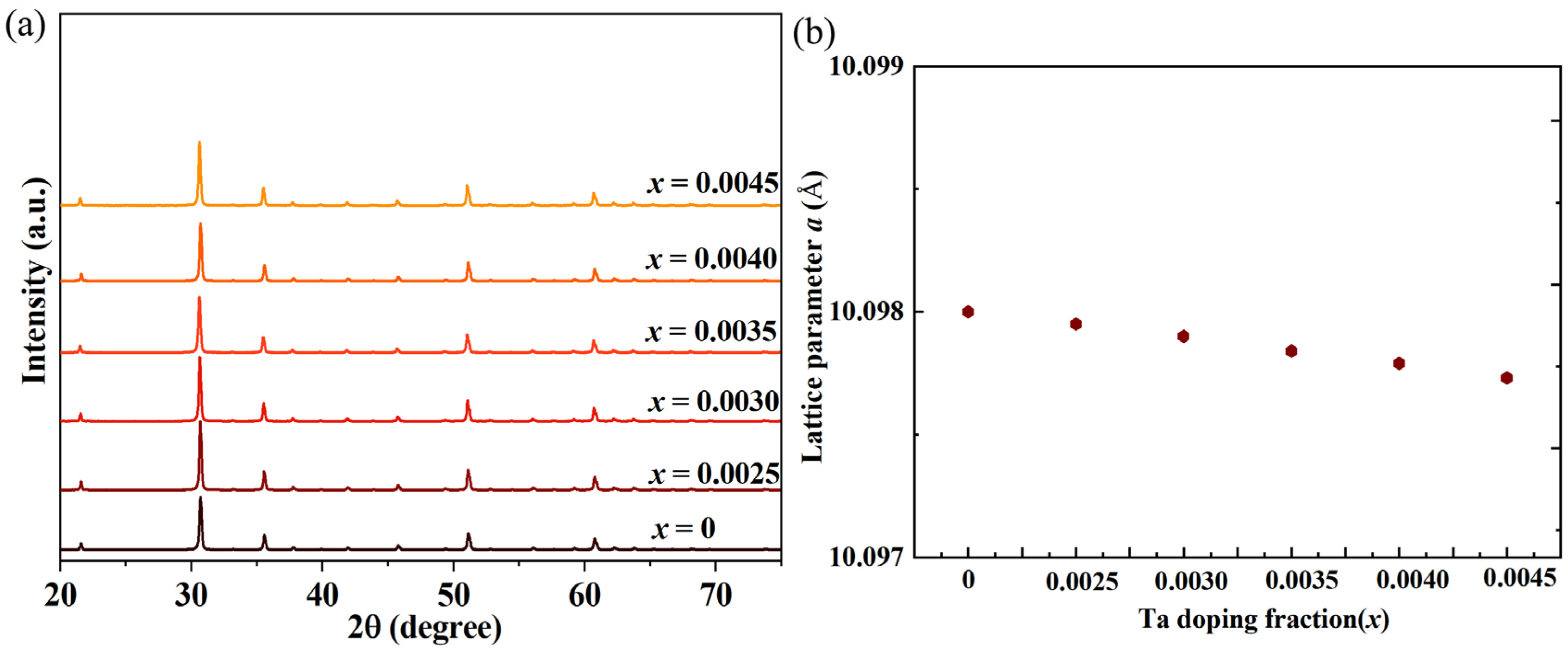
Figure 1 presents the X-ray diffraction (XRD) pattern of Tantalum (Ta)-doped indium oxide (In
2O
3). The diffraction pattern exhibits exclusively the characteristic peaks corresponding to the cubic bixbyite structure of pure In
2O
3. No extraneous peaks attributable to secondary phases, such as tantalum oxide (Ta
2O
5) or other Ta-In-O compounds, are detected within the resolution limits of the XRD instrument. The decreased lattice constants confirmed an overall contraction of the lattice constant in the Ta-doped sample compared to the pristine In
2O
3 (The Sigmas we refined are shown in
Table 1). The conjunction of phase purity and lattice contraction provides compelling evidence that Ta has been effectively incorporated into the In
2O
3 crystal structure. However, unlike the isovalent substitution seen with La
3+, the incorporation mechanism for Ta
5+ is more complex and involves aliovalent (heterovalent) substitution. This process is the primary cause of the observed lattice shrinkage. The underlying reason can be attributed to two interconnected factors: the ionic radius difference and the charge compensation mechanism. The ionic radius of the host cation In
3+ in six-fold coordination is approximately 0.80 Å. The ionic radius of the dopant cation Ta
5+ in six-fold coordination is approximately 0.64 Å. There is a significant size mismatch, with Ta
5+ being about 20% smaller than In
3+. When a smaller Ta
5+ ion directly replaces a larger In
3+ ion at its crystallographic site, it pulls the surrounding oxygen ions inward, leading to a local contraction of the lattice around the dopant atom. This direct substitution contributes to the overall reduction in lattice constant.
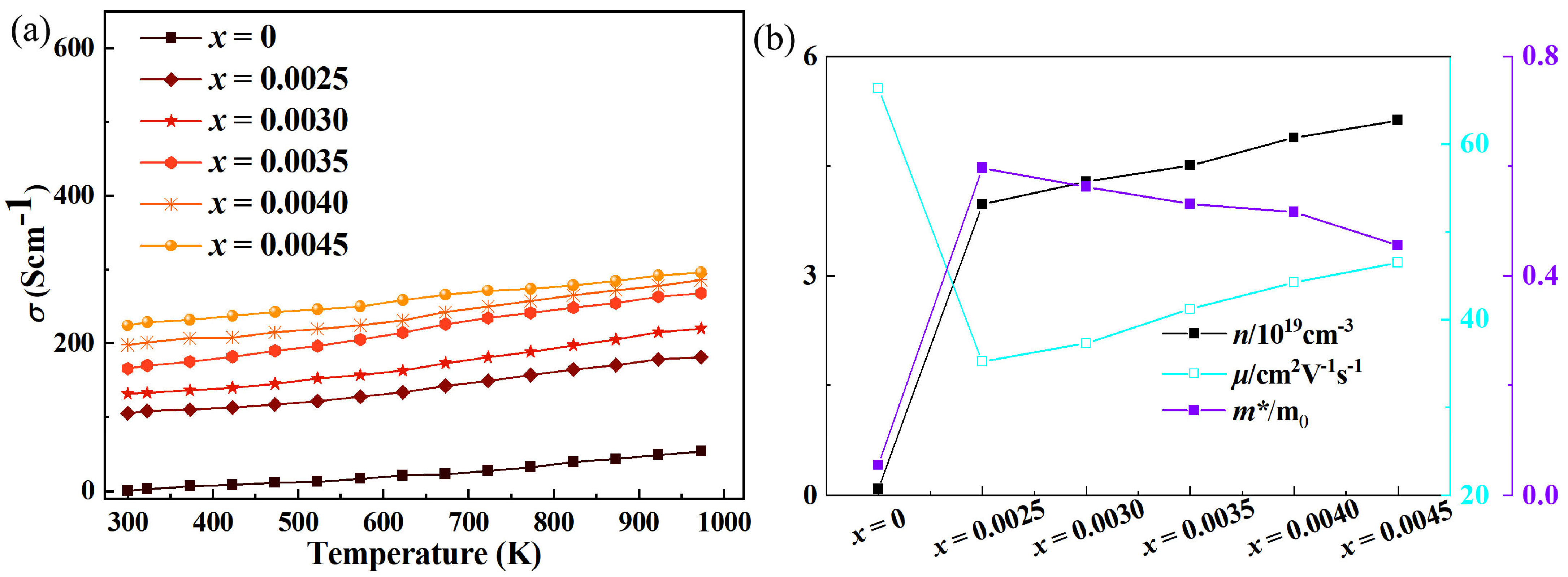
Experimental studies have found that in Ta-doped In
2O
3 thermoelectric materials, with the increase in Ta doping concentration, the electrical conductivity increases significantly, accompanied by a continuous increase in carrier concentration and a non-monotonic change in mobility (first decreasing and then increasing) as shown in
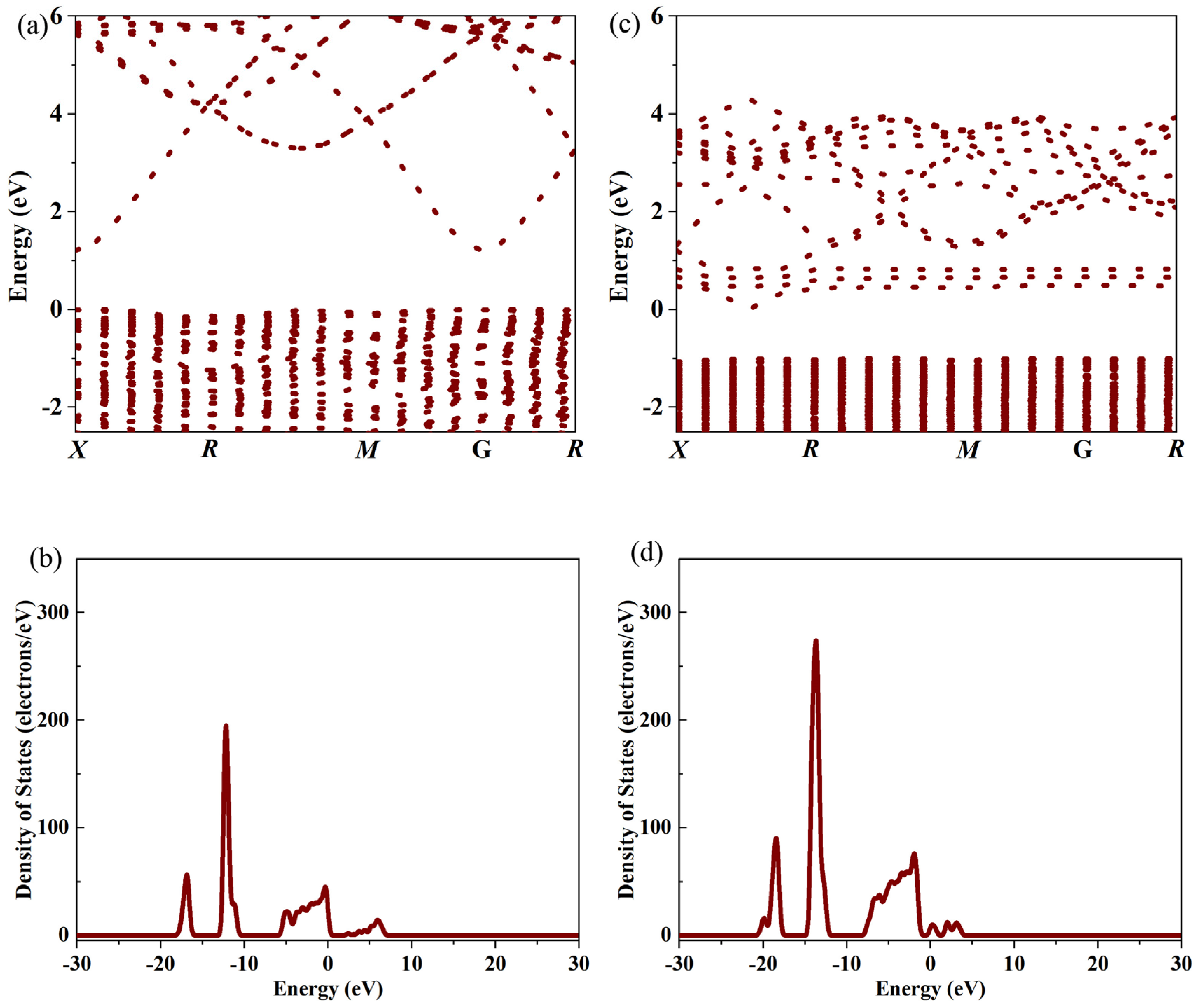
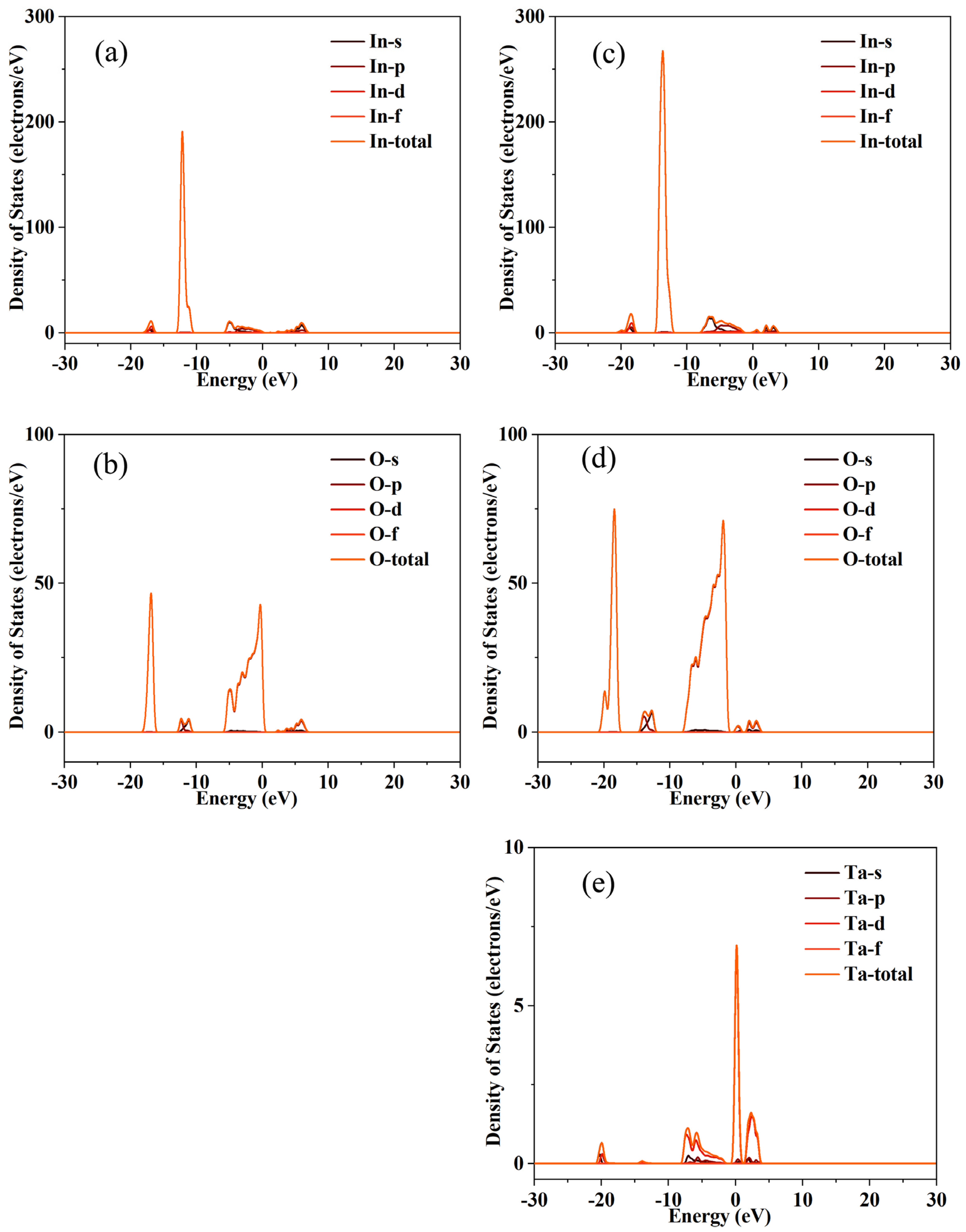
Figure 2. First-principles calculation results show that Ta doping introduces impurity levels near the Fermi level of In
2O
3, leading to a significant enhancement of the system’s density of states (DOS) as shown in
Figure 3 and
Figure 4. The crystal structure of In
2O
3 is a body-centered cubic structure (bixbyite structure) with a space group of Ia-3, where In
3+ ions occupy two different lattice sites (octahedral coordination and tetrahedral coordination), and O
2− ions form a face-centered cubic packing. The band gap of pure In
2O
3 is approximately 3.75 eV, and intrinsic carriers are mainly derived from intrinsic defects such as oxygen vacancies, whose concentration is usually low, leading to limited electrical conductivity. When Ta is doped into In
2O
3, a typical electron-doping effect occurs due to the valence difference between Ta
5+ and In
3+. When Ta
5+ substitutes for In
3+ in the In
2O
3 lattice, to maintain the electrical neutrality of the crystal, each Ta
5+ ion introduced releases two free electrons into the system. With the increase in Ta doping concentration, more and more Ta
5+ ions enter the In
2O
3 lattice, replacing the positions of In
3+, thereby continuously injecting free electrons into the system, directly leading to a significant increase in carrier concentration [
21]. Compared with carriers generated by intrinsic defects, the electron concentration introduced via doping is more precisely controllable by adjusting the doping dosage and achieves higher levels, thus serving as the primary contributor to increased carrier concentration. As a 5d-group element, tantalum (Ta) features a large atomic number, extended electron cloud distribution, and strong interactions with oxygen (O) atoms, rendering the Ta–O bond more covalent than the In–O bond. This alteration in chemical bonding facilitates electron migration within the lattice, mitigates electron localization, and further boosts carrier concentration. Notably, Ta doping does not severely compromise the crystalline integrity of In
2O
3, preserving unobstructed lattice pathways for carrier transport and providing structural support for sustained carrier concentration elevation. Mobility reflects the ease of carrier movement in the lattice and is primarily governed by lattice scattering, impurity scattering, and defect scattering. At low Ta doping concentrations, mobility decreases with increasing doping levels, mainly due to intensified impurity scattering. When Ta
5+ ions substitute In
3+ in the lattice, differences in ionic radius, atomic weight, and electronegativity between Ta
5+ and In
3+ induce local lattice distortion and potential fluctuations, which scatter moving electrons and impede their directional transport, thus reducing electron mobility. At low doping concentrations, Ta atoms exist predominantly in an isolated state, with each Ta ion acting as an independent scattering center. Higher doping concentrations increase the number of scattering centers, elevating electron-scattering center collision probability and exacerbating mobility decline. Meanwhile, the limited increase in carrier concentration partially offsets the negative impact of reduced mobility on conductivity, resulting in a moderate upward trend in conductivity. Moreover, interactions between intrinsic defects (e.g., oxygen vacancies) and Ta dopants may form composite defects, increasing lattice disorder and introducing additional electron scattering, leading to further mobility reduction. When Ta doping concentration exceeds a critical threshold, mobility increases with further doping, which is associated with lattice relaxation, impurity band formation, and scattering mechanism transformation. First, high doping concentrations enable extensive Ta
5+ incorporation into the In
2O
3 lattice; lattice self-relaxation accommodates ionic radius differences, alleviating local distortion, regularizing atomic positions, and reducing distortion-induced scattering, thus providing smoother electron transport pathways. Meanwhile, uniform Ta distribution at high doping levels avoids local ion aggregation and minimizes strong scattering center formation, further weakening impurity scattering. Second, high doping concentrations significantly increase impurity level density, forming a continuous impurity band that overlaps with the conduction band minimum. This shifts electron transport from hopping to band conduction, where electrons experience weaker scattering and exhibit higher mobility. Impurity band formation also broadens the electron transport energy range, enabling free electron movement across a wider spectrum and further improving mobility. Finally, the substantial carrier concentration increase at high doping levels enhances carrier-carrier interactions, forming an electron gas that shields the Coulomb potential field of impurity ions, weakening Coulomb scattering and reducing electron scattering probability. Additionally, high carrier concentrations mitigate phonon-induced lattice scattering, further promoting mobility improvement. In the high doping regime, improved mobility and sustained carrier concentration growth synergistically drive rapid conductivity enhancement, leading to a pronounced upward trend in conductivity with increasing doping levels. The density of states (DOS) near the Fermi level directly reflects the number of electrons that the system can accommodate at this level. Ta doping introduces impurity levels that significantly enhance the Fermi-level DOS. As Ta doping concentration rises, impurity level density increases, further enhancing the Fermi-level DOS. When DOS reaches a critical value, the Fermi level shifts toward and enters the conduction band, conferring degenerate semiconductor characteristics. In degenerate semiconductors, carrier concentration follows the Fermi-Dirac distribution instead of the Boltzmann distribution, maintaining high carrier concentrations even at room temperature. This degenerate transition further elevates the saturation carrier concentration, enabling continuous carrier concentration growth with increasing doping levels and sustaining conductivity enhancement. Additionally, enhanced DOS affects electron effective mass. Interactions between Ta-induced impurity levels and In
2O
3 conduction band states reduce electron effective mass, which facilitates higher mobility because smaller effective mass decreases electron inertial resistance in the lattice and weakens scattering effects, further promoting electron transport. Enhanced Fermi-level DOS not only increases carrier concentration but also improves electron transport efficiency. High DOS provides more electronic states near the Fermi level for electron occupation; during transport, electrons can rapidly transition to adjacent states, minimizing energy loss. Impurity levels also reduce electron localization, enhance electron cloud overlap, and promote electron delocalization, enabling free electron movement throughout the lattice and increasing transport range and rate. Furthermore, high DOS increases electron transition probability, allowing electrons to quickly find new transport pathways after scattering, reducing transmission residence time, and further improving transport efficiency. In Ta-doped In
2O
3, the synergistic effects of enhanced Fermi-level DOS, increased carrier concentration, and non-monotonic mobility variation collectively drive substantial conductivity enhancement. Particularly in the high doping regime, the significant DOS enhancement drastically improves electron transport efficiency, which, combined with high carrier concentration and improved mobility, synergistically pushes conductivity to high levels.
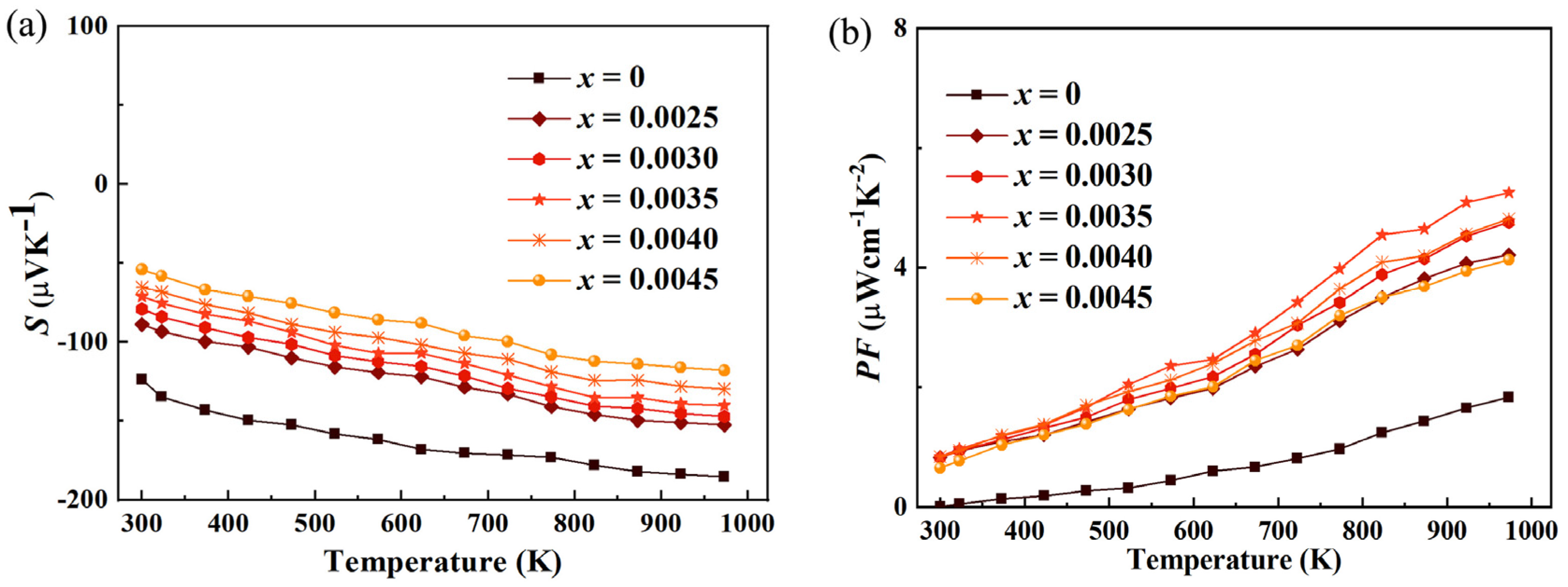
Figure 5a shows the Seebeck coefficient of Tantalum (Ta)-doped Indium Oxide (In
2O
3) thermoelectric material. It can be observed that the absolute value of the Seebeck coefficient decreases significantly after doping. This phenomenon is primarily attributed to the fundamental changes in the electrical transport properties of the material induced by doping, specifically reflected in the increased electrical conductivity, the significantly increased carrier concentration, and the potentially decreased mobility. Firstly, and most crucially, Ta doping greatly increases the carrier concentration of the material. Intrinsic indium oxide is typically an n-type semiconductor with a limited carrier concentration. When high-valence Ta
5+ ions substitute for In
3+ ions in the crystal lattice, each Ta atom contributes two extra electrons to the conduction band. This process acts as an electron doping, effectively injecting a large number of free electrons into the system. According to the fundamental formula for the Seebeck coefficient (for n-type materials, S is negative, and we discuss its absolute value), S ∝ 1/n^(2/3) (under degenerate conditions), where S is the Seebeck coefficient and n is the carrier concentration. This formula clearly indicates that the absolute value of the Seebeck coefficient is inversely proportional to the 2/3 power of the carrier concentration. Consequently, when Ta doping causes a sharp increase in n, the absolute value |S| inevitably decreases. This is the primary physical mechanism responsible for the phenomenon observed in
Figure 5. Secondly, the increase in electrical conductivity (σ) is also closely related to the decrease in the Seebeck coefficient. Electrical conductivity is determined by the formula σ = n e μ, where e is the electron charge and μ is the electron mobility. As mentioned, Ta doping significantly increases n. Even if the mobility μ decreases somewhat due to enhanced ionized impurity scattering (detailed below), the dramatic increase in n usually dominates, ultimately leading to an overall increase in electrical conductivity σ. In thermoelectric research, there is often a trade-off relationship between the Seebeck coefficient and electrical conductivity: high conductivity (implying stronger metallic character) is usually accompanied by a lower Seebeck coefficient. This is because a high density of carriers makes the asymmetry in the carrier energy distribution (i.e., the thermoelectric voltage) induced by a temperature gradient relatively smaller. Therefore, the increase in conductivity and the decrease in the Seebeck coefficient are two interconnected manifestations of the same physical process (increased carrier concentration).
In Ta-doped indium oxide materials, the significant improvement of power factor from 1.83 to 5.26 μWcm
−1K
−2 (973 K) as shown in
Figure 5b essentially results from the compensation and surpassing of the decrease in the absolute value of the Seebeck coefficient by the substantial increase in electrical conductivity. This is very competitive compared to 5.10 μWcm
−1K
−2 (973 K) for Nb doping with S = −147.05 μVK
−1, 7.76 μWcm
−1K
−2 (973 K) for V doping with S = −128.93 μVK
−1, 1.77 μWcm
−1K
−2 (973 K) for Mo doping with S = −361.23 μVK
−1 [
15,
22,
23]. Ta doping significantly increases the carrier concentration, leading to a continuous increase in carrier concentration. The enhancement of carrier concentration directly promotes a significant increase in electrical conductivity and provides core momentum for the growth of power factor. The decrease in the absolute value of the Seebeck coefficient is an inevitable consequence of the increased carrier concentration. However, the significant enhancement of the density of states near the Fermi level can mitigate the decrease in the Seebeck coefficient, avoiding excessive negative impacts on the power factor. The final improvement of power factor stems from the fact that the growth rate of electrical conductivity far exceeds the decrease rate of the square of the Seebeck coefficient. At low doping concentrations, the increase in electrical conductivity offsets the negative impact of the decreased Seebeck coefficient, resulting in a steady growth of power factor. At high doping concentrations, the electrical conductivity shows an exponential increase with the synergistic improvement of carrier concentration and mobility, while the decrease in the Seebeck coefficient tends to level off. This makes the product of S
2σ increase sharply, ultimately achieving a leapfrog growth of power factor from 1.83 for the undoped sample to 5.26 μWcm
−1K
−2 (973 K) for Ta-doped.
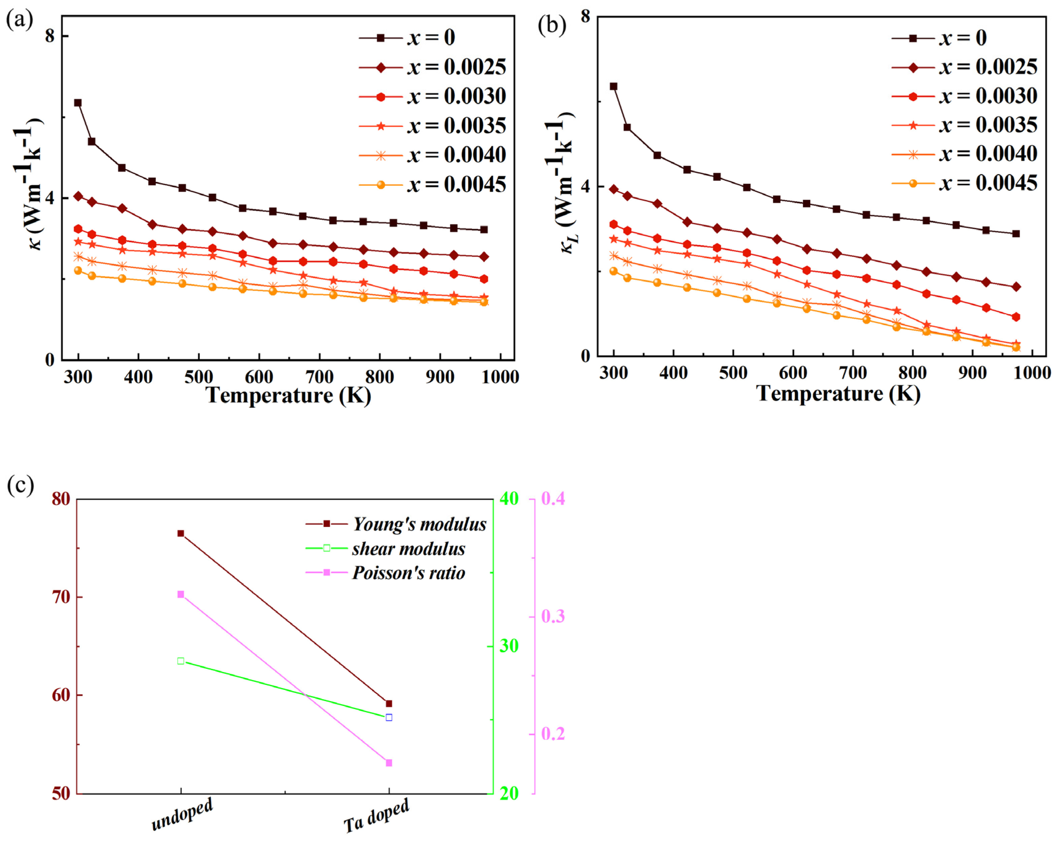
The thermal conductivity (κ) of thermoelectric materials is a key parameter determining their thermoelectric conversion efficiency, as it directly affects the temperature gradient maintenance in devices. For Ta-doped indium oxide, the overall thermal conductivity (κ) and lattice thermal conductivity (κ
L) both exhibit a significant decreasing trend with doping as shown in
Figure 6. Combined with the previously observed variations, the intrinsic mechanism of thermal conductivity reduction can be analyzed as follows. First, enhanced carrier scattering induced by lattice distortion dominates the reduction in lattice thermal conductivity. Pure indium oxide (In
2O
3) has a relatively ordered cubic bixbyite structure, and lattice thermal conductivity is mainly transmitted through phonon propagation. When Ta
5+ is doped into the In
2O
3 lattice to replace In
3+, the significant difference in ionic radius between Ta
5+ (0.064 nm) and In
3+ (0.080 nm) causes severe local lattice distortion. This distortion breaks the original periodicity of the crystal lattice, generating a large number of lattice defects such as Ta-In antisite defects, oxygen vacancies (induced by charge compensation to balance the valence difference between Ta
5+ and In
3+). These defects act as strong scattering centers for phonons: low-frequency phonons (long-wavelength phonons) are scattered by large-scale defects (e.g., dislocation clusters), while high-frequency phonons (short-wavelength phonons) are scattered by point defects (e.g., antisite defects and oxygen vacancies) [
24,
25,
26]. As a result, the mean free path of phonons is drastically shortened, and the efficiency of lattice thermal energy transmission is significantly reduced, leading to a notable decrease in κ
L. Since κ
L is the main component of κ in oxide thermoelectric materials, the reduction of κ
L directly drives the decline of κ. Second, the change in carrier transport behavior has a dual regulatory effect on thermal conductivity but does not reverse the overall downward trend. On one hand, the increase in carrier concentration (n) (consistent with the previously observed electrical conductivity enhancement) leads to a slight increase in electronic thermal conductivity (κ
e). According to the Wiedemann-Franz law, κ
e = L
0σT (where L
0 is the Lorenz number, σ is electrical conductivity, and T is absolute temperature). The elevated σ (caused by higher n) theoretically promotes κ
e. On the other hand, the reduced carrier mobility (μ) (resulting from lattice distortion and defect scattering) weakens the contribution of carriers to thermal conduction. The decrease in μ indicates that carriers (electrons) undergo more frequent collisions with defects during transport, reducing the efficiency of electronic thermal energy transmission and partially offsetting the κ
e increase caused by higher n. In Ta-doped indium oxide, the experimental results show that the increase in κ
e is far less than the decrease in κ
L. Therefore, the overall thermal conductivity still exhibits a decreasing trend. Third, the synergy between carrier transport and lattice dynamics further optimizes the thermal conductivity. The decrease in the absolute value of the Seebeck coefficient (|S|) indirectly reflects the more uniform energy distribution of carriers. Although |S| itself does not directly affect thermal conductivity, its variation is closely related to carrier concentration and mobility—key factors influencing κ
e. The higher carrier concentration (which reduces |S|) increases the number of charge carriers participating in thermal conduction, but the reduced mobility (which also correlates with |S| reduction) limits the speed of carrier thermal energy transmission. This balance between carrier quantity and transport efficiency ensures that κ
e does not become a dominant factor in κ, allowing the lattice thermal conductivity reduction to remain the main driver of overall thermal conductivity decline. This synergy is crucial for optimizing the thermoelectric performance of Ta-doped indium oxide, as it achieves a simultaneous improvement in electrical conductivity (favorable for thermoelectric efficiency) and reduction in thermal conductivity (also favorable for thermoelectric efficiency), breaking the traditional trade-off between electrical and thermal transport properties to a certain extent.
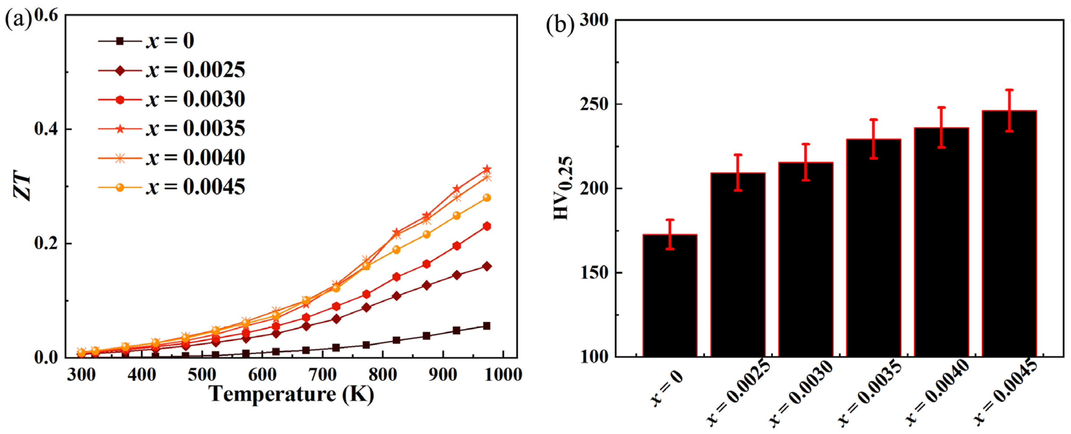
In Ta-doped indium oxide materials, the significant improvement of ZT value as shown in
Figure 7a increase in power factor and the optimized regulation of thermal conductivity, which is closely related to the modification of carrier transport properties and electronic structure. Ta doping achieves a continuous increase in carrier concentration through the electron doping effect: Ta
5+ releases free electrons when substituting In
3+, and the introduction of impurity levels reduces the electron excitation energy barrier, leading to a significant increase in carrier concentration. The enhancement of carrier concentration directly promotes a substantial increase in electrical conductivity. Although the absolute value of the Seebeck coefficient decreases due to the increase in carrier concentration, the growth rate of electrical conductivity far exceeds the decrease rate of the square of the Seebeck coefficient, ultimately achieving a significant improvement in power factor and providing core momentum for the growth of the ZT value. In addition, the impurity atoms and lattice distortions introduced by Ta doping can scatter thermal phonons, reduce the thermal conductivity, and further improve the ZT value. The leapfrog improvement of ZT value ultimately stems from the synergistic optimization of the increased power factor and reduced thermal conductivity. The significant improvement of power factor lays the foundation for the growth of ZT value, while the effective suppression of thermal conductivity amplifies this gain effect, making the ratio of (S
2σT)/κ increase sharply from 0.055 to 0.329 (973 K), which is lower than 0.42 for V dop, but higher than 0.301 for Nb doping and 0.08 for Mo doping [
15,
22,
23].
In Ta-doped indium oxide thermoelectric materials, the significant improvement of Vickers hardness as shown in
Figure 7b does not directly result from changes in electrical transport properties (such as power factor and electrical conductivity), but from the combined effects of crystal structure strengthening, chemical bond modification, and defect regulation induced by Ta doping, with an indirect correlation to the optimization of electronic structure. From the perspective of crystal structure, the ionic radius of Ta
5+ (0.064 nm) differs from that of In
3+ (0.080 nm). When Ta
5+ substitutes for In
3+ in the In
2O
3 lattice, local lattice distortion is induced. This distortion forms a “lattice stress field” that hinders the slip and movement of dislocations in the lattice, thereby enhancing the material’s resistance to plastic deformation and directly improving Vickers hardness. With the increase in doping concentration, the scope and intensity of lattice distortion gradually increase, leading to a more significant hardness enhancement effect.
The change in chemical bond characteristics is one of the core factors for hardness improvement. As a 5d transition metal element, Ta forms Ta-O bonds with O atoms that have significantly higher covalency than In-O bonds, along with higher bond energy and shorter bond length. The formation of strong covalent bonds enhances the bonding force between atoms, making the crystal structure more stable. A higher external force is required to break the interatomic bonds, resulting in a significant increase in Vickers hardness. Meanwhile, the strong interaction of Ta-O bonds inhibits the thermal vibration and diffusion of atoms, further strengthening the mechanical stability of the material. In addition, the impurity atoms and lattice defects introduced by Ta doping form a “dispersion strengthening” effect. Ta atoms are uniformly distributed in the lattice, equivalent to introducing a large number of tiny “strengthening particles” into the In2O3 matrix. These particles hinder grain boundary migration and dislocation movement, further improving the material’s hardness. The enhancement of density of states near the Fermi level reflects an increase in electron cloud overlap, indirectly indicating strengthened interatomic interactions and providing electronic structure support for hardness improvement. Ta doping significantly improves the Vickers hardness of indium oxide materials through lattice distortion strengthening, formation of strong covalent bonds, and dispersion strengthening effect. Although this change has no direct causal relationship with the optimization of electrical transport properties, both originate from the regulation of the material’s microstructure and electronic state by Ta doping, demonstrating the important role of doping modification in synchronously improving the functional characteristics and mechanical properties of thermoelectric materials.
