Abstract
Two-dimensional (2D) hybrid organic–inorganic perovskites (HOIPs) have attracted considerable attention in optoelectronic applications, owing to their remarkable characteristics. Nevertheless, the application of 2D HOIPs encounters inherent challenges due to the presence of insulating organic spacers, which create barriers for efficient interlayer charge transport (CT). To tackle this issue, we propose a BA2MAPb2I7/PEA2MA2Pb3I10 bilayer heterostructure, where efficient interlayer energy transfer (ET) facilitates compensation for the restricted charge transport across the organic spacer. Our findings reveal that under 532 nm light illumination, the BA2MAPb2I7/PEA2MA2Pb3I10 heterostructure photodetector exhibits a significant photocurrent enhancement compared with that of the pure PEA2MA2Pb3I10 device, mainly due to the contribution of the ET process. In contrast, under 600 nm light illumination, where ET is absent, the enhancement is rather limited, emphasizing the critical role of ET in boosting device performance. The overlap of the PL emission peak of BA2MAPb2I7 with the absorption spectra of PEA2MA2Pb3I10, alongside the PL quenching of BA2MAPb2I7 and the enhanced emission of PEA2MA2Pb3I10 provide confirmation of the existence of ET in the BA2MAPb2I7/PEA2MA2Pb3I10 heterostructure. Furthermore, the PL enhancement factor followed a 1/d2 relationship with the thickness of the hBN layer, indicating that ET originates from 2D-to-2D dipole–dipole coupling. This study not only highlights the potential of leveraging ET mechanisms to overcome the limitations of interlayer CT, but also contributes to the fundamental understanding required for engineering advanced 2D HOIP optoelectronic systems.
1. Introduction
Hybrid organic–inorganic perovskites (HOIPs), particularly their two-dimensional (2D) variants, have garnered significant attention in optoelectronic research due to their unique material properties. These materials exhibit strong absorption, adjustable band structures, and excellent charge transport properties like extended lifetimes and diffusion paths [1,2,3,4]. As a result, they have drawn attention for use in diverse optoelectronic platforms, including solar photovoltaics [5,6], light-emitting diodes [7,8], photodetectors [9,10], and laser sources [11,12]. Structurally, 2D HOIPs are typically represented by the formula L2An-1BnX3n+1, where the material consists of a bulky organic spacer (e.g., butylammonium (BA) or phenylethylammonium (PEA)), small organic cations (e.g., methylammonium or formamidinium), divalent metal cations (e.g., Pb2+ or Sn2+), and halide anions (e.g., Cl−, Br−, or I−), with “n” denoting the number of inorganic octahedral layers [13,14]. The modular nature of HOIPs allows for versatile band structure engineering via compositional tuning, layer thickness control, and facet exposure, offering a powerful means to optimize light–matter interactions and electronic performance. In recent years, advances in band engineering have significantly boosted charge carrier extraction for the different kinds of applications [15,16,17,18,19]. Despite these advancements, the presence of insulating organic spacers in 2D HOIP heterostructures, unlike in all-inorganic systems, poses a major challenge to efficient interlayer charge transport, thereby limiting the achievable device functionality [20,21]. Overcoming these interlayer charge transfer (CT) limitations is essential for advancing the next generation of high-efficiency 2D HOIP-based optoelectronic devices.
The interlayer CT in 2D HOIP heterostructures is hindered by the energy barriers introduced by the insulating organic spacers, which obstruct the charge movement across the interface [22]. In contrast, the interlayer energy transfer (ET) offers a potential mechanism to bypass these barriers through dipole–dipole interactions, facilitating carrier migration within the heterostructure [23]. ET occurs when an excited donor dipole transmits its energy to a neighboring acceptor dipole, provided that their emission and absorption spectra exhibit sufficient overlap [24,25]. Upon photon absorption, an electron in the donor material is excited to a higher energy state and forms an exciton by binding with a hole. This exciton can then non-radiatively transfer to a nearby acceptor through dipole–dipole coupling, with the energy being subsequently emitted as radiative light from the acceptor. This mechanism has been demonstrated to enhance the photoluminescence (PL) and improve device performance in various optoelectronic applications [22,26,27]. For instance, Luo et al. observed a significant ET effect in the WS2/CsPbBr3 heterostructures, which resulted in nearly a tenfold increase in near-infrared photodetection [28]. Recently, we found the ET effect in the BA2MA2Pb3I10/PEA2MA2Pb3I10 heterostructure, and an obvious photoresponse enhancement was observed [29]. However, research on ET processes for enhancing the performance of 2D HOIP heterostructure photodetectors remains limited. For example, the effect of n value on the ET of the BA2MAn-1PbnI3n+1/PEA2MA2Pb3I10 heterostructure and its effect on the photoresponse are still unclear, underscoring the need for further exploration.
In this study, we demonstrated that the photoresponse can be significantly enhanced in a BA2MAPb2I7/PEA2MA2Pb3I10 heterostructure photodetector via the ET process. Our findings reveal that under illumination at a wavelength of 532 nm, the heterostructure device exhibits a significant photocurrent enhancement mainly due to the contribution of ET. In contrast, under 600 nm light illumination, where the ET is absent, the photocurrent enhancement is rather limited, emphasizing the critical role of ET in boosting the device performance. In addition, the PL quenching of BA2MAPb2I7 and the enhanced emission of PEA2MA2Pb3I10, alongside the overlap of their emission and absorption spectra, provide direct evidence of efficient ET. Furthermore, we confirmed that the observed ET originates from 2D-to-2D dipole–dipole coupling. These findings highlight the potential of leveraging ET mechanisms to overcome the limitations of interlayer CT, offering a promising route toward the design of high-efficiency optoelectronic devices based on 2D HOIPs.
2. Results and Discussion
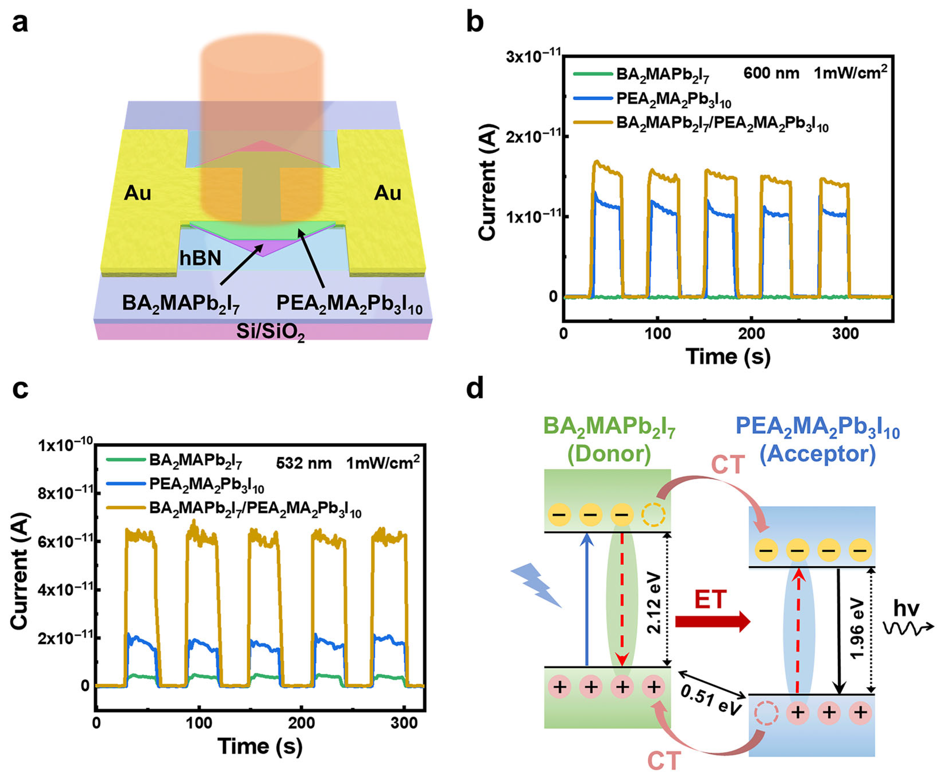
The BA2MAPb2I7 and PEA2MA2Pb3I10 crystals were synthesized using the slow cooling method described in the literature [30], and their X-ray diffraction (XRD) patterns are shown in Figure S1 (Supplementary Information). The heterostructures were fabricated via mechanical exfoliation and dry transfer, as detailed in the experimental section in the Supplementary Information. Figure 1a presents a schematic illustration of the BA2MAPb2I7/PEA2MA2Pb3I10 heterostructured device. Figure 1b,c display the current-time photoresponses of the BA2MAPb2I7/PEA2MA2Pb3I10 heterostructure, BA2MAPb2I7, and PEA2MA2Pb3I10 devices, recorded at a 1 V bias using an unfocused laser light at wavelengths of 600 nm and 532 nm with an intensity of 1 mW/cm2, respectively. The photocurrent of the heterostructure device was enhanced under both 600 nm and 532 nm light illuminations compared to the PEA2MA2Pb3I10 device. Under the 600 nm illumination, the photocurrent enhancement for the heterostructure device was modest (only 0.5 times). However, under the 532 nm illumination, the photocurrent of the heterostructure device was significantly enhanced (up to 2.7 times). This considerable discrepancy in photocurrent enhancement is unusual. The details of the photodetector properties are shown in Figure S2. To understand this, we investigated the band structure of the heterostructure. BA2MAPb2I7 and PEA2MA2Pb3I10 form a type-II heterostructure (Figure 1d), as confirmed by the absorption spectrum and ultraviolet photoelectron spectrum (Figure S3, Supplementary Information). Within a type-II heterojunction, photo-generated electrons and holes are spatially separated by the energy band offset (CT process), reducing carrier recombination and thus enhancing the photocurrent of the heterostructure device [9,31]. Although the CT process can explain some of the photocurrent enhancement, it cannot account for the significant difference observed between the 600 nm and 532 nm illuminations, suggesting the involvement of additional mechanisms. Notably, in addition to the CT, ET can also contribute to photocurrent enhancement. The BA2MAPb2I7 device exhibits no response to the 600 nm light due to its larger bandgap, which eliminates the possibility of the ET effect, leaving the photocurrent enhancement primarily attributed to CT. However, due to the insulating organic spacers, which create barriers to efficient interlayer CT, the CT effect on photocurrent enhancement is weak. In contrast, both CT and ET contribute to photocurrent enhancement under 532 nm illumination. Since the CT contribution is minimal as observed under 600 nm irradiation, the photocurrent enhancement is primarily driven by the ET process. The ET process facilitates the injection of photogenerated carriers from BA2MAPb2I7 (the donor) to PEA2MA2Pb3I10 (the acceptor) through dipole–dipole interactions (Figure 1d), significantly enhancing the photocurrent in the BA2MAPb2I7/PEA2MA2Pb3I10 heterostructure photodetector.

Figure 1.
(a) Depiction of the BA2MAPb2I7/PEA2MA2Pb3I10 heterostructure photodetector. (b) Dynamic current-time photoresponse of the BA2MAPb2I7/PEA2MA2Pb3I10 heterostructure, along with the individual BA2MAPb2I7 and PEA2MA2Pb3I10 devices, measured at a bias of 1 V under 600 nm laser illumination (unfocused, 1 mW/cm2). (c) Dynamic current-time photoresponse of the same devices recorded under 532 nm excitation at a 1 V bias, using an unfocused laser source with an identical intensity of 1 mW/cm2. (d) Schematic illustration of carrier relaxation pathways in a BA2MAPb2I7/PEA2MA2Pb3I10 heterostructure. Blue lines represent electron transitions induced by light excitation, red dashed lines indicate nonradiative recombination (on the donor side) and excitation (on the acceptor side) via ET, and the black line denotes radiative recombination.
To demonstrate the occurrence of ET in the BA2MAPb2I7/PEA2MA2Pb3I10 heterostructure, we compared the absorption spectrum of PEA2MA2Pb3I10 with the PL spectrum of BA2MAPb2I7, as shown in Figure 2a. In addition, the full-range PL and absorption spectra of BA2MAPb2I7 and PEA2MA2Pb3I10 are shown in Figure S4. The PL emission peak of BA2MAPb2I7 overlaps well with the absorption spectrum of PEA2MA2Pb3I10, suggesting that ET may occur in this heterostructure. In this system, energy emitted from BA2MAPb2I7 (the donor) could transfer to PEA2MA2Pb3I10 (the acceptor), possibly suppressing the photoluminescence of the donor and intensifying that of the acceptor. To verify this, we fabricated the BA2MAPb2I7/PEA2MA2Pb3I10 heterostructure and carried out PL measurements. Figure 2b shows an optical microscopy image of the heterostructure, accompanied by an inset showing a schematic cross-sectional view of its structure. The selection of hBN substrate was attributed to its low charge trap density, lack of dangling bonds, and atomically smooth surface [32,33]. Figure 2c presents PL spectra measured at room temperature for the BA2MAPb2I7, PEA2MA2Pb3I10, and BA2MAPb2I7/PEA2MA2Pb3I10 heterostructure. The PL peak position of the heterostructure coincides with that of PEA2MA2Pb3I10, and its PL intensity is enhanced by a factor of 2.5 relative to pristine PEA2MA2Pb3I10. This enhancement was quantitatively assessed by comparing the peak PL intensities of the heterostructure and the bare PEA2MA2Pb3I10 under identical excitation conditions, including equal illumination power and accumulation time. Conversely, the PL emission from BA2MAPb2I7 was markedly suppressed within the heterostructure. To explore the spatial characteristics of the enhanced PL signal, a PL intensity mapping of the BA2MAPb2I7/PEA2MA2Pb3I10 heterostructure was conducted, as presented in Figure 2d. In the resulting map, the red-colored region denotes the heterostructure area, while the blue region corresponds to the PEA2MA2Pb3I10 domain. The map reveals a uniform distribution of the intensified PL signal across the heterostructure region, indicating a spatially homogeneous ET process rather than a localized effect. These observations strongly support the occurrence of ET from BA2MAPb2I7 to PEA2MA2Pb3I10 within the heterostructure. It should be noted, however, that external factors, such as excitation power density [34], temperature [27], and the surrounding dielectric environment [35], may also contribute to the observed PL intensity variations.
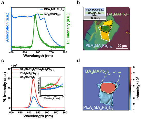
Figure 2.
(a) Normalized absorption spectrum of the PEA2MA2Pb3I10 (blue curve) and PL spectrum of BA2MAPb2I7 (green curve). (b) Optical microscopy image of the BA2MAPb2I7/PEA2MA2Pb3I10 heterojunction sample, with an inset illustrating a schematic cross-sectional view of the fabricated heterostructure. (c) PL spectra measured at room temperature for the BA2MAPb2I7, PEA2MA2Pb3I10, and the BA2MAPb2I7/PEA2MA2Pb3I10 heterostructure. (d) Spatial PL intensity distribution map of the BA2MAPb2I7/PEA2MA2Pb3I10 heterostructure, corresponding to the region shown in (b).
To rule out the possibility that experimental conditions contributed to the observed PL enhancement, we first conducted power-dependent PL measurements at room temperature within the heterostructure region. As illustrated in Figure 3a, the PL emission peak remained constant as the excitation power increased. Likewise, the full width at half maximum (FWHM) of the PL spectra, shown in Figure 3b, exhibited negligible variation with increasing power, confirming that the measurements were performed within the linear response regime of the materials. To further evaluate the influence of temperature on the PL intensity, temperature-dependent PL measurements were performed over a range from 77 K to 300 K (Figure S5, Supplementary Information). The PL enhancement factor demonstrated minimal sensitivity to temperature, remaining nearly unchanged even at 77 K (Figure 3b). Moreover, to stabilize the dielectric environment, the heterostructure was encapsulated with a thin hBN layer (Figure 3c, inset), which provides a uniform surrounding dielectric medium [35]. Notably, the PL enhancement persisted in this encapsulated configuration, reaching an enhancement factor of 7.6, which is higher than that of the BA2MA2Pb3I10/PEA2MA2Pb3I10 heterostructure [29]. We compared the PL enhancement factors of 2D heterostructures reported in recent years, which are generally in the range of 1.5 to 8 [27,28,36,37,38,39]. Collectively, these results strongly indicate that the observed PL enhancement in the BA2MAPb2I7/PEA2MA2Pb3I10 heterostructure originates from the interlayer ET process, rather than from external experimental variables.
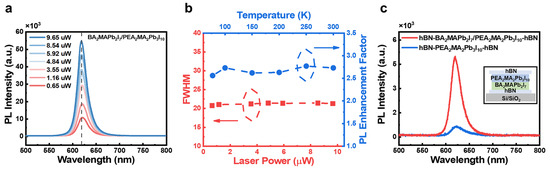
Figure 3.
(a) PL spectra of the BA2MAPb2I7/PEA2MA2Pb3I10 heterostructure under varying excitation powers. (b) Evolution of the PL emission full width at half maximum (FWHM) with increasing laser power (red curve), accompanied by the temperature-dependent trend in the PL enhancement factor (blue curve). (c) PL spectra of the BA2MAPb2I7/PEA2MA2Pb3I10 heterostructure encapsulated with an hBN layer; the inset presents a schematic cross-sectional view of the device structure.
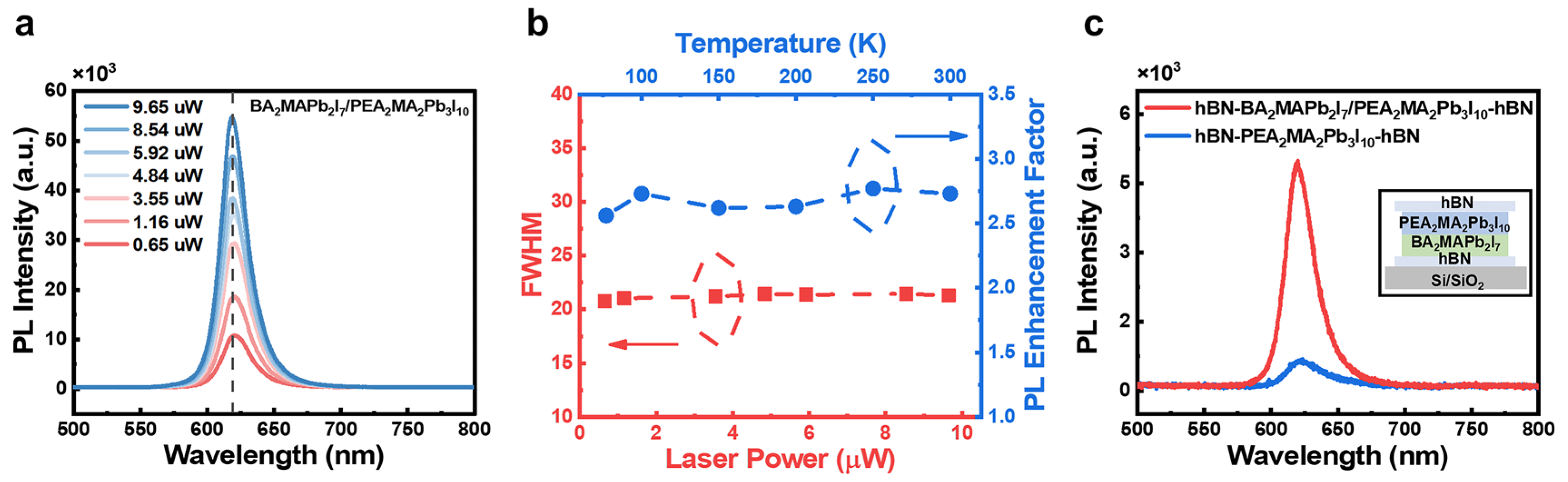
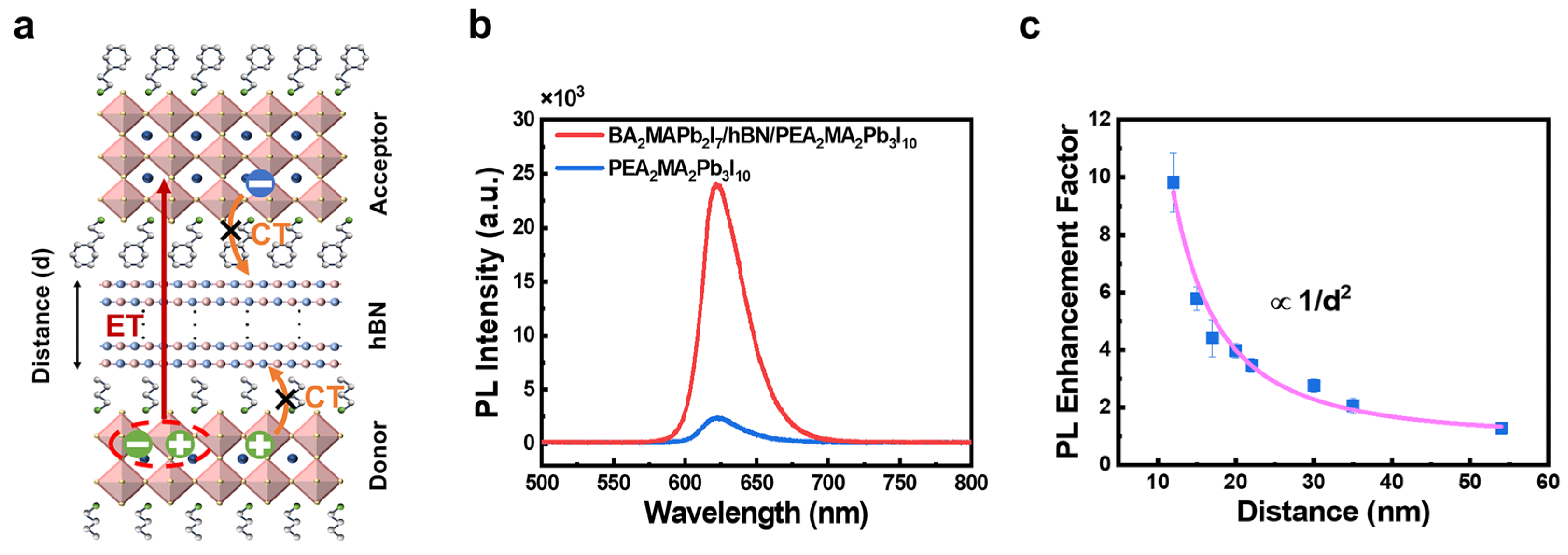
Generally, observing dipole–dipole coupling in type-II heterostructures is challenging as a result of the spatial separation between electrons and holes. However, in the BA2MAPb2I7/PEA2MA2Pb3I10 heterostructure, the insulating organic spacer helps suppress the separation of these pairs, potentially facilitating dipole–dipole interactions. To gain deeper insight into the dipole–dipole coupling between the donor and acceptor within the heterostructure, a charge-blocking hBN layer was inserted, as depicted in Figure 4a. If the CT process is inhibited by this interlayer, we would expect the PL emission to be further enhanced in the BA2MAPb2I7/hBN/PEA2MA2Pb3I10 heterostructure compared to the BA2MAPb2I7/PEA2MA2Pb3I10 heterostructure. Indeed, the PL enhancement factor of the BA2MAPb2I7/hBN/PEA2MA2Pb3I10 heterostructure reaches 10.2, as shown in Figure 4b (with an 11 nm-thick hBN layer, Figure S6, Supplementary Information), significantly higher than that of the BA2MAPb2I7/PEA2MA2Pb3I10 heterojunction as shown in Figure 2b. Furthermore, based on the principles of ET theory, the efficiency of ET is inversely proportional to the thickness of the charge-blocking interlayer (d, in this case, the hBN layer) between the donor and acceptor layers, following a 1/dn relationship. Here, n depends on the system’s dimensionality: n = 6 for 0D-0D dipole–dipole interactions, n = 4 for 0D-2D dipole–dipole interactions, and n = 2 for 2D-2D dipole–dipole interactions [40,41]. As shown in Figure 4c, the PL enhancement factor, which serves as an indicator of ET efficiency, exhibits a 1/d2 decay with increasing interlayer thickness in the heterostructure. This behavior suggests that the ET process between BA2MAPb2I7 and PEA2MA2Pb3I10 is governed by 2D-to-2D dipole–dipole coupling, consistent with similar findings in ReS2/hBN/MoSe2 heterostructures [36].

Figure 4.
(a) Diagram illustrating the incorporation of an hBN interlayer within the heterostructure to suppress the charge transfer (CT) process. (b) PL spectra collected from the PEA2MA2Pb3I10 and BA2MAPb2I7/hBN/PEA2MA2Pb3I10 regions on an hBN substrate. (c) Dependence of the PL enhancement factor on the interlayer spacing, represented by the hBN thickness, exhibiting a 1/d2 dependence.
3. Materials and Methods
3.1. Synthesis and Sample Preparation
First, lead iodide (461 mg), methylamine iodide (79.6 mg), and n-butylamine iodide (174.8 mg) were combined in a mixture of 50% hydroiodic acid (1.44 mL) and 50% hypophosphorous acid solution (0.16 mL). This mixture underwent heating to 120 °C under continuous stirring until boiling commenced, and the temperature was sustained for 1 min to achieve complete dissolution. Gradual cooling to 25 °C followed to encourage crystallization. The crystals produced were cleaned using a dichloromethane solution, moved to a 30 °C heating table, and dried for 10 min, yielding BA2MAPb2I7 crystals.
Subsequently, a solution was prepared by dissolving lead iodide (461 mg), methylamine iodide (105.8 mg), and phenylethylamine iodide (69.2 mg) in 50% hydroiodic acid (1.08 mL) and 50% hypophosphorous acid solution (0.12 mL). Continuous stirring accompanied heating to 120 °C, bringing the mixture to a boil; full dissolution was ensured by maintaining this temperature for 1 min. Slow cooling to 25 °C was then implemented to facilitate crystallization. After rinsing with dichloromethane solution, the resulting crystals were transferred onto a heating table at 30 °C and dried for 10 min to obtain dry PEA2MA2Pb3I10 crystals.
3.2. Heterostructure Fabrication
hBN nanosheets were mechanically exfoliated and transferred onto a Si/SiO2 substrate using a PDMS stamp. Similarly, BA2MAPb2I7 and PEA2MA2Pb3I10 nanosheets were exfoliated from bulk crystals and transferred onto PDMS stamps. A custom-designed precision transfer stage was used to accurately position the selected BA2MAPb2I7 nanosheet onto the hBN layer. Following this, a PEA2MA2Pb3I10 nanosheet was carefully placed on top of the BA2MAPb2I7 nanosheet to form the BA2MAPb2I7/PEA2MA2Pb3I10 heterostructure. Throughout the transfer procedure, precise alignment was ensured using optical microscopy.
3.3. Characterization
BA2MAPb2I7 and PEA2MA2Pb3I10 crystals underwent an X-ray diffraction (XRD) analysis on a Bruker D8 (Bremen, Germany) diffractometer equipped with monochromatized Cu Kα radiation (λ = 1.5406 Å). UV-Vis absorbance data were acquired using an Agilent Cary 5000 spectrophotometer (San Jose, CA, USA). Photoluminescence (PL) characterization employed a 532 nm Horiba Scientific laser source (Singapore). Cryogenic PL evaluations required mounting samples in a liquid-nitrogen-cooled continuous-flow cryostat. For the PL excitation, the 532 nm laser was focused via a 100× objective lens (NA = 0.80). Ultraviolet photoelectron spectroscopy (UPS) measurements performed on an ESCALAB 250XI (Waltham, MA, USA) system established the work function and valence band positions of both crystals. Surface topography was imaged by atomic force microscopy (AFM) using the BRUKER MultiMode8 intelligent scanning mode for precision-enhanced data collection.
3.4. Device Fabrication and Characterization
Following mechanical exfoliation and transfer, PEA2MA2Pb3I10 nanosheets were stacked onto BA2MAPb2I7 nanosheets to form the heterostructure. Subsequently, 50 nm-thick gold (Au) electrodes were fabricated via direct current magnetron sputtering with a custom shadow mask. Following this, hBN nanosheets were then transferred over the BA2MAPb2I7/PEA2MA2Pb3I10 heterostructure using an identical transfer protocol to that applied for PEA2MA2Pb3I10. A room-temperature optoelectronic characterization of the photodetectors was conducted employing a Keithley 4200A-SCS semiconductor parameter analyzer coupled to a probe station. Illumination during testing utilized unfocused 532 nm and 600 nm laser sources.
4. Conclusions
In summary, we introduced a novel approach to enhance the photodetection of 2D HOIP photodetectors through exploiting the interlayer ET within a BA2MAPb2I7/PEA2MA2Pb3I10 heterostructure. It was found that under 532 nm light illumination, our heterostructure device achieves a substantial photocurrent enhancement of 2.7 times compared with that of the pure PEA2MA2Pb3I10 device, driven by the contribution of ET. Conversely, under 600 nm light illumination, where ET is absent, the enhancement is limited, highlighting the pivotal role of ET in enhancing device performance. The overlap of the PL emission peak of BA2MAPb2I7 with the absorption spectra of PEA2MA2Pb3I10, alongside the PL quenching of BA2MAPb2I7 and the enhanced emission of PEA2MA2Pb3I10 provides confirmation of the existence of ET in the BA2MAPb2I7/PEA2MA2Pb3I10 heterostructure. The heterostructure exhibits a 7.6-fold photoluminescence (PL) enhancement relative to isolated PEA2MA2Pb3I10, even in the absence of a charge-blocking layer. When charge transfer (CT) processes were suppressed through the hBN interlayer insertion, the PL emission in the heterostructure region exceeded one order of magnitude. Furthermore, the PL enhancement factor followed a 1/d2 relationship with the thickness of the hBN layer, indicating ET originates from 2D-to-2D dipole–dipole coupling. This study not only establishes a deeper understanding of ET in 2D HOIP heterostructures, but also contributes to the fundamental understanding required for engineering advanced 2D HOIP optoelectronic systems.
Supplementary Materials
The following supporting information can be downloaded at: https://www.mdpi.com/article/10.3390/inorganics13070240/s1. Figure S1: The XRD patterns of BA2MAPb2I7 (a) and PEA2MA2Pb3I10 (b) crystals; Figure S2: (a) I–V curve of heterostructure in darkness and under different light intensities. (b) Photoswitching characteristics measured at 1 V under 532 nm light illumination with light intensity ranging from 5 to 1000 µW/cm2. (c) The power-dependent responsivity and specific detectivity under a bias of 1 V. (d) Response speed of the BA2MAPb2I7/PEA2MA2Pb3I10 heterostructure photodetector under a bias of 1 V; Figure S3: Tauc plots (a) and UPS spectrum (b) of BA2MAPb2I7, Tauc plots (c) and UPS spectrum (d) of PEA2MA2Pb3I10; Figure S4: (a) PL spectroscopy and (b) ultraviolet absorption spectroscopy of BA2MAPb2I7, (c) PL spectroscopy and (d) ultraviolet absorption spectroscopy of PEA2MA2Pb3I10. Figure S5: Temperature-dependent PL spectra were recorded for the PEA2MA2Pb3I10 and BA2MAPb2I7/PEA2MA2Pb3I10 heterostructure regions; Figure S6: AFM images of the hBN layer inserted between BA2MAPb2I7 and PEA2MA2Pb3I10 are presented, with the inset showing the corresponding height profile. References [42,43] are cited in the Supplementary Materials.
Author Contributions
B.H.: conceptualization (lead), data curation (lead); writing—original draft (lead). B.L.: data curation (equal). Q.Q.: data curation (equal). X.L.: data curation (equal). Y.T.: data curation (equal). M.L.: data curation (equal). S.D.: writing—review and editing (equal). B.X.: writing—review and editing (equal). All authors have read and agreed to the published version of the manuscript.
Funding
This work was financially supported in part by the National Natural Science Foundation of China (Grant No. 51901119), the excellent innovation team plan of XianYang (Grant No. L2024-CXNL-KJRCTD-KJ TD-0016), the fund for Shanxi “1331 Project”, Shanxi “Academician reserve candidate”.
Institutional Review Board Statement
Not applicable.
Informed Consent Statement
Not applicable.
Data Availability Statement
The data that support the findings of this study are available within the article and its Supplementary Material.
Conflicts of Interest
The authors declare no conflicts of interest.
References
- Shrestha, S.; Li, X.; Tsai, H.; Hou, C.-H.; Huang, H.-H.; Ghosh, D.; Shyue, J.-J.; Wang, L.; Tretiak, S.; Ma, X.; et al. Long Carrier Diffusion Length in Two-Dimensional Lead Halide Perovskite Single Crystals. Chem 2022, 8, 1107–1120. [Google Scholar] [CrossRef]
- Kong, L.; Zhang, X.; Li, Y.; Wang, H.; Jiang, Y.; Wang, S.; You, M.; Zhang, C.; Zhang, T.; Kershaw, S.V.; et al. Smoothing the Energy Transfer Pathway in Quasi-2D Perovskite Films Using Methanesulfonate Leads to Highly Efficient Light-Emitting Devices. Nat. Commun. 2021, 12, 1246. [Google Scholar] [CrossRef] [PubMed]
- Wang, R.; Dong, X.; Ling, Q.; Fu, Q.; Hu, Z.; Xu, Z.; Zhang, H.; Li, Q.; Liu, Y. Spacer Engineering for 2D Ruddlesden–Popper Perovskites with an Ultralong Carrier Lifetime of Over 18 Μs Enable Efficient Solar Cells. ACS Energy Lett. 2022, 7, 3656–3665. [Google Scholar] [CrossRef]
- Mandal, A.; Roy, S.; Mondal, A.; Gupta, S.; Pal, B.; Bhattacharyya, S. Spacer Switched Two-Dimensional Tin Bromide Perovskites Leading to Ambient-Stable Near-Unity Photoluminescence Quantum Yield. J. Phys. Chem. Lett. 2022, 13, 9103–9113. [Google Scholar] [CrossRef]
- Li, D.; Xing, Z.; Meng, X.; Hu, X.; Hu, T.; Chen, Y. Spontaneous Internal Encapsulation via Dual Interfacial Perovskite Heterojunction Enables Highly Efficient and Stable Perovskite Solar Cells. Nano Lett. 2023, 23, 3484–3492. [Google Scholar] [CrossRef]
- Zhao, D.; Gao, D.; Wu, X.; Li, B.; Zhang, S.; Li, Z.; Wang, Q.; Wu, Z.; Zhang, C.; Choy, W.C.H.; et al. Efficient and Stable 3D/2D Perovskite Solar Cells through Vertical Heterostructures with (BA)4AgBiBr8 Nanosheets. Adv. Mater. 2022, 34, 2204661. [Google Scholar] [CrossRef]
- Sun, C.; Jiang, Y.; Cui, M.; Qiao, L.; Wei, J.; Huang, Y.; Zhang, L.; He, T.; Li, S.; Hsu, H.-Y.; et al. High-Performance Large-Area Quasi-2D Perovskite Light-Emitting Diodes. Nat. Commun. 2021, 12, 2207. [Google Scholar] [CrossRef] [PubMed]
- Mishra, J.K.; Yantara, N.; Kanwat, A.; Furuhashi, T.; Ramesh, S.; Salim, T.; Jamaludin, N.F.; Febriansyah, B.; Ooi, Z.E.; Mhaisalkar, S.; et al. Defect Passivation Using a Phosphonic Acid Surface Modifier for Efficient RP Perovskite Blue-Light-Emitting Diodes. ACS Appl. Mater. Interfaces 2022, 14, 34238–34246. [Google Scholar] [CrossRef]
- Han, B.; Liu, B.; Wang, G.; Qiu, Q.; Wang, Z.; Xi, Y.; Cui, Y.; Ma, S.; Xu, B.; Hsu, H.-Y. Transparent and Reusable Nanostencil Lithography for Organic–Inorganic Hybrid Perovskite Nanodevices. Adv. Funct. Mater. 2023, 33, 2300570. [Google Scholar] [CrossRef]
- Wang, G.; Han, B.; Mak, C.H.; Liu, J.; Liu, B.; Liu, P.; Hao, X.; Wang, H.; Ma, S.; Xu, B.; et al. Mixed-Dimensional van Der Waals Heterostructure for High-Performance and Air-Stable Perovskite Nanowire Photodetectors. ACS Appl. Mater. Interfaces 2022, 14, 55183–55191. [Google Scholar] [CrossRef]
- Bera, K.P.; Hanmandlu, C.; Lin, H.-I.; Ghosh, R.; Gudelli, V.K.; Lai, C.-S.; Chu, C.-W.; Chen, Y.-F. Fabry–Perot Oscillation and Resonance Energy Transfer: Mechanism for Ultralow-Threshold Optically and Electrically Driven Random Laser in Quasi-2D Ruddlesden–Popper Perovskites. ACS Nano 2023, 17, 5373–5386. [Google Scholar] [CrossRef] [PubMed]
- Lei, L.; Dong, Q.; Gundogdu, K.; So, F. Metal Halide Perovskites for Laser Applications. Adv. Funct. Mater. 2021, 31, 2010144. [Google Scholar] [CrossRef]
- Pan, D.; Fu, Y.; Spitha, N.; Zhao, Y.; Roy, C.R.; Morrow, D.J.; Kohler, D.D.; Wright, J.C.; Jin, S. Deterministic Fabrication of Arbitrary Vertical Heterostructures of Two-Dimensional Ruddlesden-Popper Halide Perovskites. Nat. Nanotechnol. 2021, 16, 159–165. [Google Scholar] [CrossRef]
- Rahil, M.; Ansari, R.; Prakash, C.; Islam, S.; Dixit, A.; Ahmad, S. Ruddlesden–Popper 2D Perovskites of Type (C6H9C2H4NH3)2(CH3NH3)n−1PbnI3n+1 (n = 1–4) for Optoelectronic Applications. Sci. Rep. 2022, 12, 2176. [Google Scholar]
- Gao, C.; Jia, S.; Yin, X.; Li, Z.; Yang, G.; Chen, J.; Li, Z.; An, X. Enhancing Open-Circuit Voltage in FAPbI3 Perovskite Solar Cells via Self-Formation of Coherent Buried Interface FAPbIx Cl3−x. Chem. Commun. 2025, 61, 2758–2761. [Google Scholar] [CrossRef]
- Zhu, B.; Wang, Z.; Zhang, Y.; Yu, Z.; Shi, J.; Xiong, R. Low Temperature Fabrication of the Giant Dielectric Material CaCu3Ti4O12 by Oxalate Coprecipitation m Ethod. Mater. Chem. Phys. 2009, 113, 746–748. [Google Scholar] [CrossRef]
- Li, N.; Hu, X.; Tang, Y.; Lei, Y.; Suet Lau, Y.; Chen, Q.; Sui, X.; Zhu, F. Perovskite/Organic Tandem Device to Realize Light Detection and Emission Dual Function. Chem. Eng. J. 2024, 490, 151573. [Google Scholar] [CrossRef]
- Jia, S.; Li, Y.; Gao, C.; Liu, G.; Ren, Y.; He, C.; An, X.-T. Realization of P-Type MA-Based Perovskite Solar Cells Based on Exposure of the (002) Facet. Appl. Phys. Lett. 2025, 126, 023908. [Google Scholar] [CrossRef]
- Zhu, B.P.; Guo, W.K.; Shen, G.Z.; Zhou, Q.; Shung, K.K. Structure and Electrical Properties of (111)-Oriented Pb(Mg1/3Nb2/3)O3-PbZrO3-PbTiO3 Thin Film for Ultra-High-Frequency Transducer Applications. IEEE Trans. Ultrason. Ferroelectr. Freq. Control 2011, 58, 1962–1967. [Google Scholar] [CrossRef]
- Min, L.; Tian, W.; Cao, F.; Guo, J.; Li, L. 2D Ruddlesden–Popper Perovskite with Ordered Phase Distribution for High-Performance Self-Powered Photodetectors. Adv. Mater. 2021, 33, 2101714. [Google Scholar]
- Zhang, F.; Lu, H.; Tong, J.; Berry, J.J.; Beard, M.C.; Zhu, K. Advances in Two-Dimensional Organic-Inorganic Hybrid Perovskites. Energy Environ. Sci. 2020, 13, 1154–1186. [Google Scholar]
- Han, B.; Qiu, Q.; Tang, Y.; Lian, B.; Liu, B.; Ding, S.; Ma, S.; Luo, M.; Wang, W.; Xu, B.; et al. Manipulating Interlayer Carrier Relaxation Dynamics in Type-II Heterostructures of 2D Hybrid Perovskites Through Organic Spacer Engineering. Adv. Funct. Mater. 2024, 35, 2417167. [Google Scholar] [CrossRef]
- Hu, Z.; Liu, X.; Hernandez-Martinez, P.L.; Zhang, S.; Gu, P.; Du, W.; Xu, W.; Demir, H.V.; Liu, H.; Xiong, Q. Interfacial Charge and Energy Transfer in van Der Waals Heterojunctions. InfoMat 2022, 4, e12290. [Google Scholar] [CrossRef]
- Li, C.; Loh, K.; Leng, K. Organic-Inorganic Hybrid Perovskites and Their Heterostructures. Matter 2022, 5, 4153–4169. [Google Scholar] [CrossRef]
- Song, Y.; Zhang, C.; Liu, W.; Li, X.; Long, H.; Wang, K.; Wang, B.; Lu, P. High-Efficiency Energy Transfer in Perovskite Heterostructures. Opt. Express 2018, 26, 18448–18456. [Google Scholar] [CrossRef]
- Cheng, C.; Li, Z.; Hambarde, A.; Deotare, P. Efficient Energy Transfer across Organic–2D Inorganic Heterointerfaces. ACS Appl. Mater. Interfaces 2018, 10, 39336–39342. [Google Scholar] [CrossRef]
- Zhang, Q.; Linardy, E.; Wang, X.; Eda, G. Excitonic Energy Transfer in Heterostructures of Quasi-2D Perovskite and Monolayer WS2. ACS Nano 2020, 14, 11482–11489. [Google Scholar] [CrossRef]
- Luo, Z.; Yi, X.; Jiang, Y.; Luo, N.; Liu, B.; Zhong, Y.; Tan, Q.; Jiang, Q.; Liu, X.; Chen, S.; et al. Efficient Energy Transfer Enabled by Dark States in van Der Waals Heterostructures. ACS Nano 2024, 18, 31215–31224. [Google Scholar] [CrossRef]
- Han, B.; Tang, Y.; Qiu, Q.; Lian, B.; Liu, B.; Ding, S.; Ma, S.; Li, G.; Xu, B.; Hsu, H.-Y. Enhancing Photodetector Performance via Interlayer Energy Transfer in 2D Hybrid Perovskite Heterostructures. J. Phys. D Appl. Phys. 2025, 58, 135115. [Google Scholar] [CrossRef]
- Sheng, S.; Li, Y.; Xia, M.; Shi, E. Quasi-2D Halide Perovskite Crystals and Their Optoelectronic Applications. J. Mater. Chem. A 2022, 10, 19169–19183. [Google Scholar] [CrossRef]
- Pan, B.; Dou, Z.; Su, M.; Li, Y.; Wu, J.; Chang, W.; Wang, P.; Zhang, L.; Zhao, L.; Zhao, M.; et al. Direct Selective Epitaxy of 2D Sb2Te3 onto Monolayer WS2 for Vertical p–n Heterojunction Photodetectors. Nanomaterials 2024, 14, 884. [Google Scholar] [CrossRef]
- Fu, L.; Sun, Y.; Wu, N.; Mendes, R.; Chen, L.; Xu, Z.; Zhang, T.; Rümmeli, M.; Rellinghaus, B.; Pohl, D.; et al. Direct Growth of MoS2/h-BN Heterostructures via a Sulfide-Resistant Alloy. ACS Nano 2016, 10, 2063–2070. [Google Scholar] [CrossRef] [PubMed]
- Wang, Q.; Wee, A. Photoluminescence Upconversion of 2D Materials and Applications. J. Phys.-Condens. Mat. 2021, 33, 223001. [Google Scholar]
- Kaplan, D.; Gong, Y.; Mills, K.; Swaminathan, V.; Ajayan, P.M.; Shirodkar, S.; Kaxiras, E. Excitation Intensity Dependence of Photoluminescence from Monolayers of MoS2 and WS2/MoS2 Heterostructures. 2D Mater. 2016, 3, 015005. [Google Scholar] [CrossRef]
- Raja, A.; Waldecker, L.; Zipfel, J.; Cho, Y.; Brem, S.; Ziegler, J.D.; Kulig, M.; Taniguchi, T.; Watanabe, K.; Malic, E.; et al. Dielectric Disorder in Two-Dimensional Materials. Nat. Nanotechnol. 2019, 14, 832–837. [Google Scholar] [CrossRef]
- Karmakar, A.; Al-Mahboob, A.; Petoukhoff, C.E.; Kravchyna, O.; Chan, N.S.; Taniguchi, T.; Watanabe, K.; Dani, K.M. Dominating Interlayer Resonant Energy Transfer in Type-II 2D Heterostructure. ACS Nano 2022, 16, 3861–3869. [Google Scholar] [CrossRef]
- Karmakar, A.; Kazimierczuk, T.; Antoniazzi, I.; Raczyński, M.; Park, S.; Jang, H.; Taniguchi, T.; Watanabe, K.; Babiński, A.; Al-Mahboob, A.; et al. Excitation-Dependent High-Lying Excitonic Exchange via Interlayer Energy Transfer from Lower-to-Higher Bandgap 2D Material. Nano Lett. 2023, 23, 5617–5624. [Google Scholar] [CrossRef]
- Karmakar, A.; Al-Mahboob, A.; Zawadzka, N.; Raczyński, M.; Yang, W.; Arfaoui, M.; Gayatri; Kucharek, J.; Sadowski, J.T.; Shin, H.S.; et al. Twisted MoSe2 Homobilayer Behaving as a Heterobilayer. Nano Lett. 2024, 24, 9459–9467. [Google Scholar] [CrossRef]
- Li, Y.; Zeng, Y.; Ou, Z.; Dai, W.; Wang, C.; Li, Z.; Li, W.; Yan, J.; Yu, S.; Yu, Y.; et al. Tunability of the Energy Transfer Process in Type-II Heterostructures. ACS Photonics 2024, 11, 3722–3729. [Google Scholar] [CrossRef]
- Lin, T.N.; Huang, L.T.; Shu, G.W.; Yuan, C.T.; Shen, J.L.; Lin, C.A.J.; Chang, W.H.; Chiu, C.H.; Lin, D.W.; Lin, C.C.; et al. Distance Dependence of Energy Transfer from InGaN Quantum Wells to Graphene Oxide. Opt. Lett. 2013, 38, 2897. [Google Scholar] [CrossRef] [PubMed]
- Itskos, G.; Heliotis, G.; Lagoudakis, P.G.; Lupton, J.; Barradas, N.P.; Alves, E.; Pereira, S.; Watson, I.M.; Dawson, M.D.; Feldmann, J.; et al. Efficient Dipole-Dipole Coupling of Mott-Wannier and Frenkel Excitons in (Ga, In) N Quantum Well/Polyfluorene Semiconductor Heterostructures. Phys. Rev. B 2007, 76, 035344. [Google Scholar] [CrossRef]
- Wang, K.; Wu, C.; Yang, D.; Jiang, Y.; Priya, S. Quasi-Two-Dimensional Halide Perovskite Single Crystal Photodetector. ACS Nano 2018, 12, 4919–4929. [Google Scholar] [CrossRef]
- Peng, W.; Yin, J.; Ho, K.; Ouellette, O.; De Bastiani, M.; Murali, B.; El Tall, O.; Shen, C.; Miao, X.; Pan, J.; et al. Ultralow Self-Doping in Two-Dimensional Hybrid Perovskite Single Crystals. Nano Lett. 2017, 17, 4759–4767. [Google Scholar] [CrossRef]

Disclaimer/Publisher’s Note: The statements, opinions and data contained in all publications are solely those of the individual author(s) and contributor(s) and not of MDPI and/or the editor(s). MDPI and/or the editor(s) disclaim responsibility for any injury to people or property resulting from any ideas, methods, instructions or products referred to in the content. |
© 2025 by the authors. Licensee MDPI, Basel, Switzerland. This article is an open access article distributed under the terms and conditions of the Creative Commons Attribution (CC BY) license (https://creativecommons.org/licenses/by/4.0/).