Review

A Study on the Multifunctional Properties and Application Perspectives of ZnO/SiC Composite Materials

by
Mohammad Nur-E-Alam
1,2,3
1
School of Science, Edith Cowan University, 270 Joondalup Drive, Joondalup, WA 6027, Australia
2
Institute of Sustainable Energy, Universiti Tenaga Nasional, Jalan Ikram-Uniten, Kajang 43000, Selangor, Malaysia
3
Centre for Promotion of Research, Graphic Era (Deemed to Be University), Clement Town, Dehradun 248002, India
Inorganics 2025, 13(7), 235; https://doi.org/10.3390/inorganics13070235
Submission received: 14 May 2025 / Revised: 11 June 2025 / Accepted: 7 July 2025 / Published: 10 July 2025
(This article belongs to the Section Inorganic Materials)

Abstract

ZnO/SiC nanocomposite materials possess significant potential for various technological fields due to their extraordinary optical, electrical, thermal, and mechanical properties. The synthesis methods, material properties, and diverse applications of ZnO/SiC composites have been systematically explored in this study. The potential application areas of this nanocomposite include their roles in photocatalysis, optoelectronic devices, gas sensors, and photovoltaic systems. The synergetic effects of ZnO and SiC are analyzed to highlight their advantages over their individual components. Future research directions must focus on the remaining challenges to optimize these nanoscale composite materials for industrial and emerging applications.

1. Introduction

ZnO and SiC are widely recognized for their unique properties, making them suitable for various industrial applications. ZnO, a wide bandgap semiconductor, is well-known for its high exciton binding energy and excellent optoelectronic properties. ZnO is also highly acceptable to researchers for its low toxicity, thermal stability, and cost-effectiveness, and it can be extensively used in optical, electronic, and biochemical applications. However, its wide band gap (~3.37 eV) limits visible light absorption and promotes electron recombination [1,2,3,4,5]. To conquer these limitations, doping with non-metals (e.g., N, C, S), metal ions (e.g., Ca, Mn, Co, Ni, Al, Ga), or rare earth (RE) metals has been explored to reduce ZnO’s band gap and enhance its optical properties. RE metals possess unique electronic configurations, effectively capturing photogenerated carriers, preventing electron–hole recombination, and extending light absorption into the visible range [5,6,7,8,9,10,11]. However, the functionality of ZnO thin films is somehow dependent on their fabrication processes, which are mostly selected based on the application types, as the material crystallinity, adhesion, and durability are critically important for those nanotechnological applications. Therefore, tailoring the properties of ZnO thin films by employing various fabrication methods and optimization of process parameters has been one of the most widely studied areas for more than a decade [9,12,13,14,15,16].
On the other hand, SiC (a compound of silicon and carbon) is highly regarded for its superior thermal stability and mechanical strength. SiC is also known as a wide bandgap semiconductor material with the composition-dependent bandgap shaping possibility that makes it attractive for optoelectronic applications [17]. The composition-dependent bandgap tunability of SiC allows for shaping electronic and optical properties, essentially effective for advanced photonic integrated circuit (PIC) development. Additionally, SiC exhibits a high optical refractive index and significant second- and third-order nonlinearities, enabling its use in nonlinear optics and quantum photonics applications, including quantum sensing. In particularly, 4H–SiC material supports various photonic building blocks, such as confined waveguides, beam splitters, optical parametric oscillators, optical frequency combs, and modulators [18,19,20]. Amorphous SiC thin films are well-suited for integrated optics devices due to their low-temperature deposition capability on diverse substrates and tunability of composition adjustment to obtain the desired application-specific physical, optical, electronic, and tribological properties. For example, hydrogenated amorphous SiC films enable efficient doping and introduce novel properties, influenced by deposition methods and post-processing like annealing [18]. SiC thin films are known for high hardness, low thermal expansion, chemical inertness, oxidation resistance, and high thermal conductivity, which make them an extremely durable encapsulating layer with the capability of effectively dissipating heat without subjecting the devices to severe chemical, thermal, and mechanical environments. It is widely utilized in abrasive materials, high-efficiency brake disks, drill bits, and fire-retardant films. In integrated circuitry (IC) applications, SiC functions as a diffusion barrier, protective coating, and interlevel dielectric, ensuring reliable performance at high temperatures and electric fields. Its application extends to insulated gate bipolar transistors (IGBTs) in electric vehicle (EV) power systems, promoting energy-efficient power electronics. Furthermore, SiC facilitates its integration into optical and optoelectronic devices, including passivation coatings for LEDs, optical waveguides, planar optical systems, flexible electroluminescent panels, window protection, and passivation in thin-film solar cells [18,19,20,21,22,23,24,25].
Recent nanomaterials research trends found that composite materials have revolutionized materials science and engineering due to the potential to combine the separate features of technologically significant constituent materials [26,27,28,29,30]. The combination of ZnO and SiC in composite form (yet to be explored further) presents a promising avenue for enhancing the performance of existing materials in various applications, particularly in high-temperature environments and energy conversion technologies. ZnO/SiC composites synthesized via different fabrication techniques exhibit the formation of a superior material layer interface effective for UV radiation protection and outstanding performance (comparatively higher transparency and a specific type of conductivity) to be used as electron transport layers (ETL) in thin-film solar cells [30,31]. Worth noting is that while Reference [31] provides a comprehensive experimental analysis of ZnO/SiC thin films, this review goes much beyond that contribution, with greater inclusion of the literature, critical evaluation of multifunctional properties, and exploration of potential applications, particularly in optoelectronics, photovoltaics, sensing, and high-temperature electronics. This review aims to provide a comprehensive understanding of ZnO/SiC composite materials, focusing on their synthesis methods and practical applications.
In the review, ZnO/SiC is used to denote composite materials in which ZnO and SiC are either mixed or co-deposited to form a mixed-phase material, while ZnO–SiC explicitly denotes layered heterojunction structures with definite interfaces. The term nanocomposites is generically employed to cover thin films and bulk materials in which either ZnO, SiC, or both the components have structural features at the nanometer scale. Unless otherwise mentioned, ZnO/SiC composites in this paper mean both thin-film and bulk composites with functional integration of ZnO and SiC phases.

2. Materials Synthesis Methods

Several methods have been developed for synthesizing thin-film nanomaterials and various nanocomposite layers, each offering distinct advantages in tailoring the material properties.

2.1. Sol–Gel Methods

The sol–gel method is a widely used approach due to its cost-effectiveness and ability to achieve high-purity materials. In essence, the sol–gel approach is a chemo-mechanical procedure. A suspension of colloidal particles, which are submicron or nanometric in size, is called a sol. A condensation reaction forms interparticle connections if the particles have surface-active groups, such as hydroxyls. A mildly stiff substance called a gel is created if the condensation process is such that the solvent is trapped in the matrix of sol particles or the evolved by-product, which may include hydrogen gas (H2), depending on the specific chemical precursor reactions. It is not required to begin with a colloidal suspension alone; a colloidal particle production can be an intermediary step. For instance, to fabricate ZnO/SiC composite layers, the respective composite powders (prepared by blending ZnO microspheres with different amounts of SiC NC suspension using ball-mill processing) were coated onto the substrates (like ceramic tubes equipped with gold electrodes for the development of a sensor) followed by a thermal treatment process (cured at 150 °C for 1 h) [32,33,34]. In the sol–gel method, the final material’s composition, structure, and properties can be precisely controlled by tailoring parameters such as precursor concentration, pH, reaction temperature, and aging time.

2.2. Chemical Vapor Deposition (CVD)

CVD allows for precise control over the composition and microstructure of ZnO/SiC composites. ZnO/SiC composite films have been successfully synthesized using various Chemical Vapor Deposition (CVD) techniques, each offering distinct advantages in tailoring structural, optical, and electrical properties. Aerosol-Assisted CVD (AACVD) enables low-temperature growth of Si-doped ZnO films with high optical transparency (72–80%) and significantly enhanced conductivity (resistivity reduced to 2.0 × 10⁻² Ω·cm at 4 mol% Si), attributed to optimal dopant incorporation, as confirmed by XRD and XPS analyses [35]. Metal–Organic CVD (MOCVD) and Atmospheric Pressure MOCVD (APMOCVD) have been employed for epitaxial ZnO growth on SiC substrates, where substrate orientation and the use of a buried insulating layer improve crystallinity and excitonic emission, as verified by Photoluminescence (PL) and XRD measurements [36,37,38]. Low-Pressure CVD (LPCVD) allows for defect and morphology control through precise regulation of stoichiometry and reaction kinetics, enabling the fabrication of transparent and fluorescent ZnO films [39]. Plasma-Enhanced CVD (PE-CVD) facilitates the growth of c-axis-oriented ZnO nanorod arrays at relatively low temperatures (200–300 °C), demonstrating excellent structural and luminescent properties, as confirmed by FE-SEM, XPS, and PL analyses [40]. Across these techniques, deposition temperature plays a pivotal role, influencing nucleation density, grain size, and electrical conductivity. Optimal growth temperatures range from 350 °C to 825 °C, depending on the technique, with AACVD showing best results at 450 °C and MOCVD typically requiring higher temperatures [41,42,43]. Additionally, thermal management in CVD reactors—enhanced by CFD simulations—has been crucial for achieving uniform deposition and high-quality films in batch processes involving SiC coatings on graphite substrates [44,45].
This technique is beneficial for producing thin films and coatings with enhanced durability and performance.

2.3. Mechanical Processing via Bead Milling

Bead milling is a top-down mechanical technique extensively used in particle size reduction and homogenous dispersion of nanoparticles. For ZnO/SiC composites, bead milling is used to disperse SiC nanoparticles in a ZnO powder matrix to create a physically mixed composite precursor. Although no new phase occurs, the process is advantageous for creating fine and uniform powder mixtures for subsequent sintering or film deposition. The “ZnO matrix” here refers to ZnO as the continuous phase for further processing operations [46]. For example, an elevation in milling velocity can markedly enhance the specific surface area of the powder from 0.0643 to 3.59 m2/g [47], thereby facilitating the creation of nanoscale structures. The integration of SiC within ZnO matrices has demonstrated a significant enhancement in the gas sensing efficacy for nitrogen monoxide (NO), achieving detection thresholds as minimal as 100 ppb [33], while concurrently improving mechanical attributes such as plasticity, toughness, and wear resistance in zinc–aluminum-based composites [48]. Moreover, combining mechanical milling with methodologies such as sonication-assisted exfoliation can produce ZnO-based composites exhibiting superior structural properties [49]. Nevertheless, obstacles such as ensuring homogeneous nanoparticle dispersion and preserving composite stability remain, frequently necessitating meticulous optimization of milling parameters, particularly in the context of secondary materials like graphite, which can influence the dispersion of ZnO crystallites [50].

2.4. Hydrothermal Synthesis

Hydrothermal synthesis is the crystallization of materials from high-temperature aqueous solutions under moderate-to-high pressure in a sealed autoclave. This environment encourages slow and controlled nucleation and growth of nanostructures that can quite frequently result in well-defined morphologies and improved crystallinity even at comparatively low temperatures. This technique has attracted significant attention in thin films and composite materials synthesis, as this method offers numerous advantages. For example, this method offers low-temperature processing, which preserves the structural integrity of fragile SiC substrates while enabling the deposition of highly crystalline ZnO films [51]. Other works reported that this method provides precise control over the morphology of ZnO structures—i.e., the formation of vertically aligned nanorod arrays—thereby enhancing the surface area, light absorption, and charge carrier dynamics that are crucial for photocatalytic and optoelectronic performance [52,53]. The coupling of SiC and ZnO also facilitates internal metal–semiconductor junctions, which contribute to efficient charge separation and reducing recombination, greatly improving the photocatalytic degradation efficiency under UV or visible light illumination [54,55]. Additionally, ZnO/SiC composites also exhibit superior optical properties with increased transmittance and decreased reflectance, making them immensely appropriate for high-sensitivity photodetectors capable of performing in unfavorable, high-temperature conditions [53]. Aside from optoelectronics, ZnO–SiC-based nanomaterials have demonstrated promising non-toxic antitumor activities, prefiguring their potential for biomedical uses [56]. Nevertheless, problems concerning the achievement of uniform thickness of films, scalability, and alignment of nanostructures over large areas in hydrothermal synthesis remain open for refinement and technological advancement.

2.5. E-Beam and Thermal Evaporation

Electron beam (E-beam) evaporation is a physical vapor deposition (PVD) technique in which a concentrated electron beam is used to locally heat and evaporate source materials of high purity in a vacuum chamber. The atoms evaporated from the source are condensed on a substrate in the form of a thin film. E-beam evaporation allows precise control of film composition and thickness and is well-suited to refractory or complex oxide materials such as ZnO. Thermal evaporation, on the other hand, involves resistive or inductive heating of the source material to the vaporization point. The vapor travels through a low-pressure ambience and condenses on cooler substrate surfaces. Although simpler to establish, thermal evaporation typically results in less energetic species and is optimally used for volatile or low-melting-point materials.
E-beam and thermal evaporation deposition methods offer precise control of film thickness, uniformity, and composition, which are the most important parameters for device performance optimization. E-beam evaporation is demonstrated to be efficient in the fabrication of high-purity ZnO thin films with high uniformity and controllable structural and electrical properties, and high applicability to advanced optoelectronic devices [57]. Thermal evaporation, which is commonly employed for SiC films, enables the formation of high-quality crystalline structures essential for heterojunction solar cell efficiency improvement [58]. ZnO–SiC heterojunctions fabricated using these techniques exhibit strong rectifying behavior and strong electroluminescence with characteristic emission peaks at 410 nm, rendering them suitable for light-emitting applications [57]. Additionally, ZnSiO composite thin films deposited by hybrid evaporation methods present compact morphologies and adjustable physical properties, widening their applications in a variety of technological domains [59]. In photovoltaic devices, ZnO–SiC–Si heterojunction solar cells have demonstrated significantly enhanced photoelectric conversion efficiencies, which can be up to twice the level of conventional solar architectures [58]. Moreover, ZnO-decorated SiC composites have also exhibited excellent electromagnetic wave absorption performance with high reflection losses, indicating their potential for stealth and electromagnetic shielding applications [28]. Despite these developments, challenges relating to the optimization of film growth parameters, homogeneous integration of materials, and full comprehension of interfacial mechanisms governing device performance remain fundamental areas that need to be addressed through further research and development.

2.6. Radio Frequency (RF) Magnetron Co-Sputtering

This technique is a versatile method for producing thin films and coatings, including metal oxides and dielectrics (e.g., ZnO, SiC, and ZnO/SiC composite thin films), with enhanced durability and performance for potential applications in electronics, photovoltaics, and optoelectronics [31,60,61,62]. RF co-sputtering allows precise control of the deposition process, enabling the tailoring of film properties through adjustments in sputtering power, gas flow, and substrate conditions. For example, ZnO/SiC composite films with a tunable bandgap of 3.3 eV to 3.8 eV, formed by changing the SiC sputtering power from 10 to 30 W, have been promoted as potential electron transport layers for perovskite solar cells. Electrical characterization through Hall effect measurements confirmed n-type conductivity, where carrier concentration and charge transfer efficiency were optimized at 20 W SiC power [31]. ZnO thin films deposited on silicon substrates with a pure form showed a crystallite size of approximately 108.16 nm, low surface roughness, and resistivity between 1 and 100 Ω·cm, which are preferable characteristics for the development of high-quality devices [63]. Incorporation of SiC in ZnO not only improved the structural quality of films but also improved crystallinity and reduced defect densities, particularly at the optimized sputtering conditions [63]. Furthermore, research on co-doping methods, such as Al and Si co-doped ZnO, has demonstrated the potential for further enhancement in electrical properties, suggesting that a broader investigation of composite material systems may result in thin films with enhanced functionality for future photovoltaic and electronic devices [64]. A comparative overview of the key synthesis methods, their features, and application areas is summarized in Table 1.

3. Properties of ZnO/SiC Composites

This section provides a concise overview of the development history of ZnO/SiC nanocomposites and their experimental results, interpretation, as well as the conclusions.

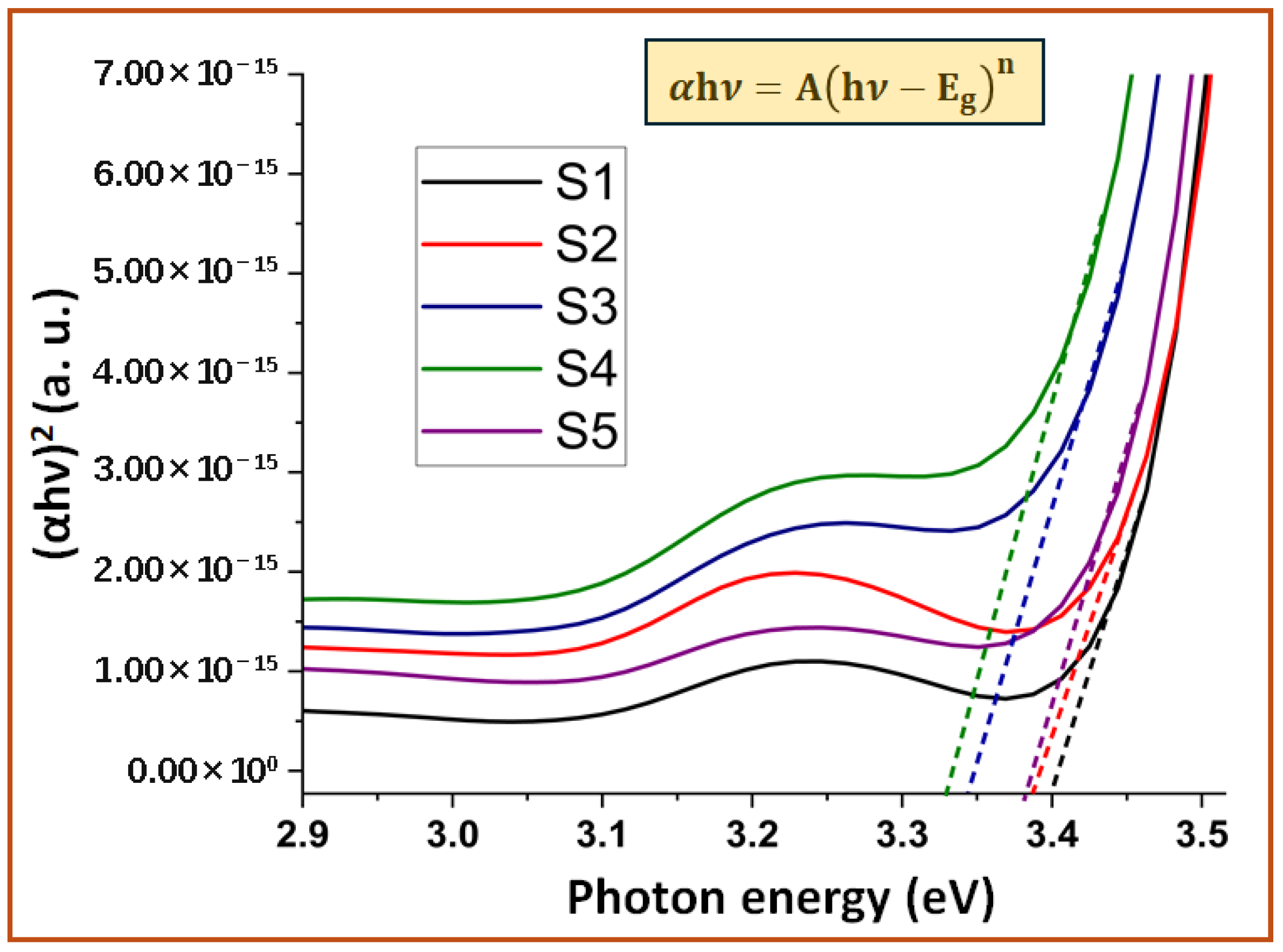
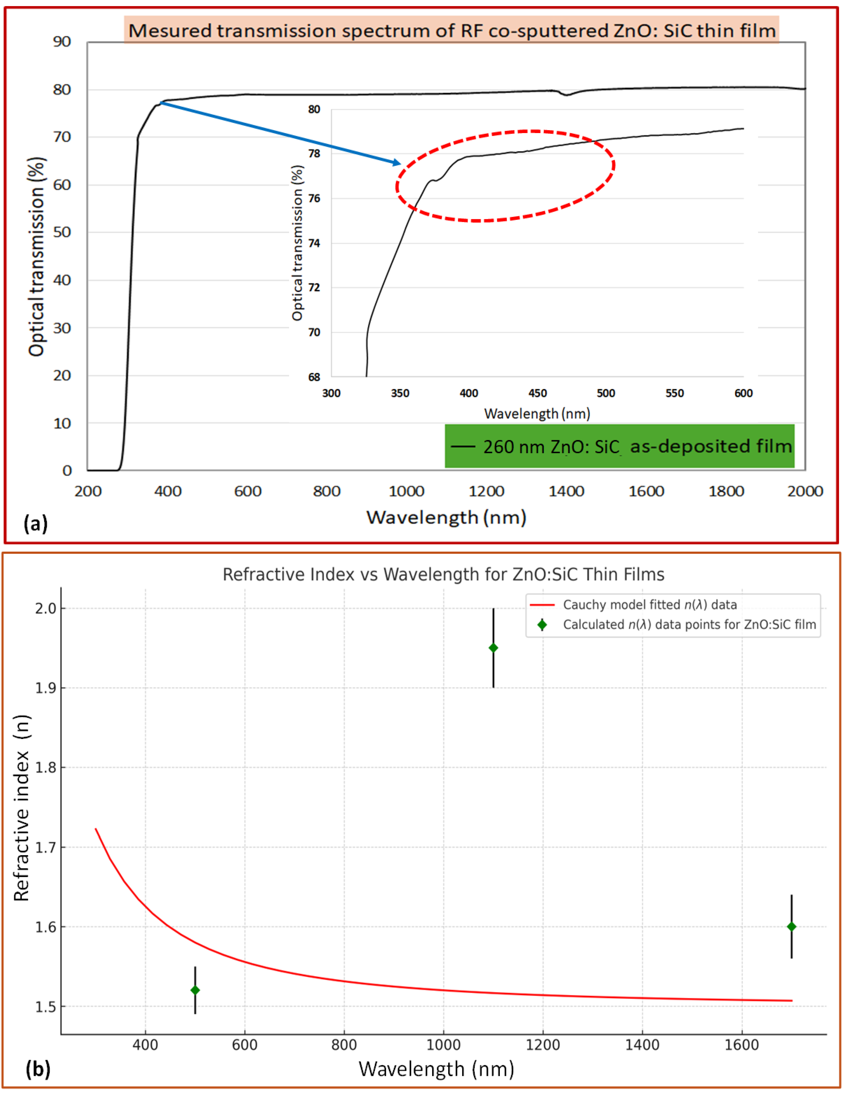
3.1. Optical Properties

The optical properties of ZnO/SiC composite thin films are significantly influenced by the incorporation of silicon carbide, which alters the electronic structure and enhances their suitability for optoelectronic and photovoltaic applications. These composites typically exhibit a tunable optical bandgap in the range of 3.3 to 3.5 eV (shown in Figure 1), depending on the SiC content and sputtering conditions, which can be optimized for visible and near-UV light absorption. UV–Vis spectroscopy analyses confirm increased transmittance in the visible range and reduced reflectance based on the volumetric content of SiC during the co-sputtered development of the composite films, which are advantageous for selecting the right choice of film composition to enhance light harvesting in solar cells [31].
Moreover, the refractive index and extinction coefficient values can be modulated with varying SiC concentrations, enabling better control over optical interference effects in multilayer devices. The refractive index values, extracted from transmittance spectra using envelope and Swanepoel methods (Figure 2), indicate a dispersion trend consistent with wide-bandgap semiconductors. The refractive index decreases with increasing wavelength, which is characteristic of normal dispersion behavior. This optical response can be attributed to the combined effects of ZnO’s intrinsic properties and the presence of SiC nanoparticles, which may modify the dielectric environment and interfacial polarization within the film matrix. The measured transmission spectrum (Figure 2a) of the 260 nm thick film reveals high transparency across the visible to near-infrared region (NIR), with optical transmittance exceeding 75% in the 400–1600 nm range. A pronounced and relatively sharp absorption edge is observed near 380 nm, indicating a low density of sub-bandgap defect states and suggesting good optical quality. The inset plot further highlights this sharp rise in transmission, which may point to improved crystallinity and reduced structural disorder, potentially influenced by the incorporation of SiC nanoparticles into the ZnO matrix. Figure 2b presents the refractive index (n) as a function of wavelength, derived from the Swanepoel envelope method using the transmission data. The calculated data points, fitted with a Cauchy dispersion model, show a normal dispersion trend with decreasing n as wavelength increases, characteristic of dielectric materials. The refractive index ranges approximately from 2.1 in the NIR to about 1.5 in the visible range. While these values are within expected ranges for ZnO-based nanocomposites, they may also reflect porosity or partial amorphization within the film due to sputtering conditions. It should be noted that the refractive index data points are limited in number, and the observed deviations from the fitted model at some wavelengths, along with the size of the associated error bars, suggest a need for further measurements with higher spectral resolution. Moreover, this result assumes a homogeneous and isotropic film, whereas the actual film may exhibit inhomogeneities, interface effects, or anisotropy due to nanostructuring and the presence of SiC. Therefore, while the results are promising and indicate favorable optical properties, additional characterization, such as spectroscopic ellipsometry and high-resolution structural analysis, is necessary to fully confirm and validate the optical constants and to better understand the impact of SiC incorporation on the refractive index behavior of ZnO/SiC thin films. However, this moderate variation in refractive index suggests potential applicability in antireflective coatings and electron transport layers in optoelectronic devices, particularly perovskite solar cells and UV photodetectors.
The addition of SiC nanoparticles into the ZnO matrix is expected to reduce defect states and improve crystallinity, which could result in sharper absorption edges and lower Urbach energy, indicators of decreased disorder in the films. Although direct studies on the impact of SiC incorporation into ZnO matrices on Urbach energy are currently limited, analogous research on other ZnO-based composites supports this possibility. For instance, CeO2 addition to ZnO has been shown to sharpen absorption edges and lower Urbach energy, reflecting reduced structural disorder [65]. Consequently, further targeted investigations are necessary to conclusively determine whether SiC incorporation produces similar enhancements in ZnO/SiC thin films.
The optical properties of ZnO/SiC composite thin films are also highly influenced by SiC, which alters the electronic structure and renders them more viable for optoelectronic and photovoltaic applications. Experiments conducted by Li et al. [63] and Felix et al. [56] corroborate that sputtering power and defect chemistry play pivotal roles in adjusting optical bandgaps and light transmission. In addition, the ZnO mixtures with rare earth elements or Si-containing compounds have demonstrated improved light absorption and reduced Urbach energy [36,65]. All these reports reinforce the importance of compositional engineering in tuning optical responses.

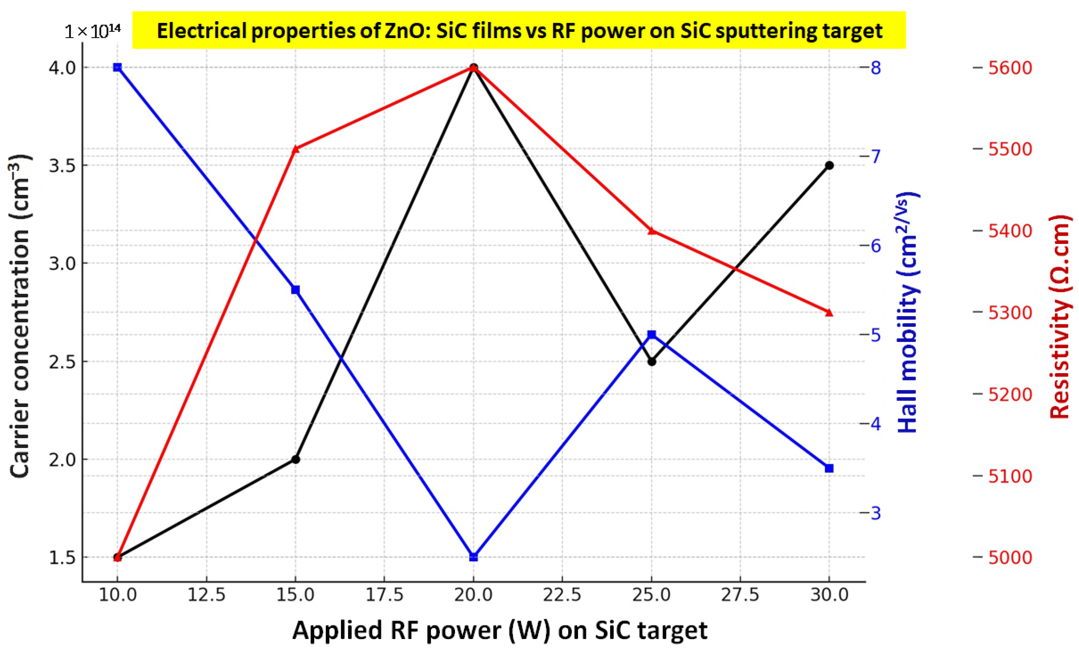
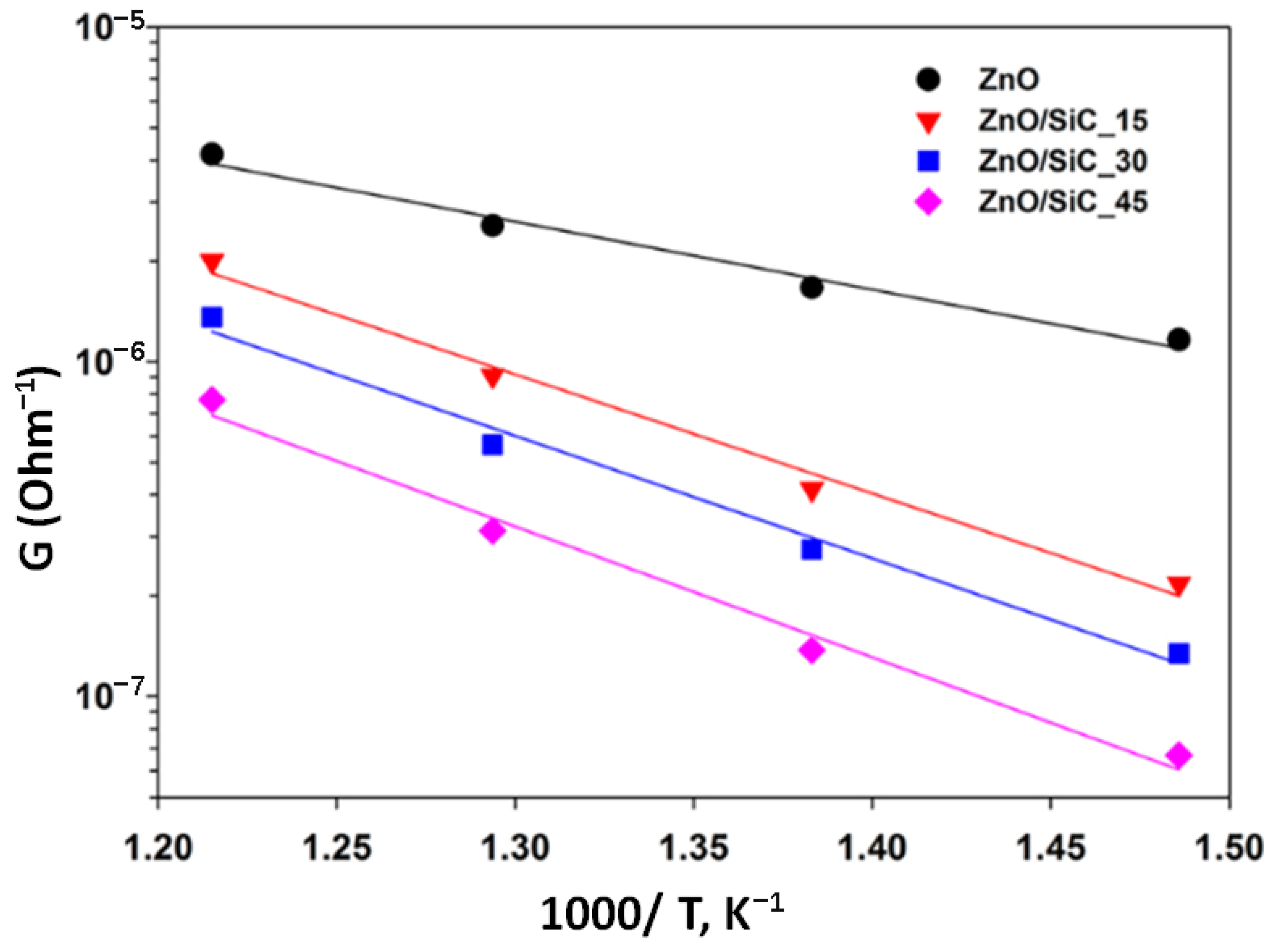
3.2. Electrical Properties

The electrical properties of ZnO/SiC composite thin films have been found to be promising for application in advanced optoelectronic devices. ZnO, an intrinsic n-type semiconductor, when combined with SiC nanoparticles, known for their wide bandgap and excellent thermal stability, exhibits modified electrical behavior, enhancing its applicability in diodes, photodetectors, and light-emitting devices. These composites display strong rectifying characteristics, with reported leakage currents below 1 nA at reverse biases of −3 V and ideality factors ranging from 1.13 to 1.52, indicating efficient charge transport mechanisms [56,66]. Figure 3 illustrates the electrical and optoelectronic performance of ZnO/SiC heterojunctions. The current-voltage (I–V) characteristics across different temperatures (Figure 3a) show thermally enhanced current transport, while the capacitance-voltage (C–V) behavior (Figure 3b) supports a well-defined depletion region. Figure 3c demonstrates enhanced photocurrent under illumination, with anisotropic junctions showing better performance. The band alignment in Figure 3d confirms favorable offsets for charge transfer. Electroluminescence results in Figure 3e reveal strong visible emission with peaks shifting and varying in intensity with temperature.
The current-voltage studies show forward currents between 0.8 and 10 mA at 8 V and on–off current ratios up to ~107, while reverse currents remain in the picoampere range [67,68], confirming their low power consumption and diode-like performance. Furthermore, electroluminescence from ZnO/SiC heterostructures is observed in the UV and visible regions, notably around 410 nm, with additional bands attributed to defect-related emissions. The inclusion of SiC may aid in passivating grain boundaries and suppressing oxygen-related defects, which enhances carrier mobility and reduces resistivity. However, challenges remain, particularly in achieving reliable p-type conductivity in ZnO, which limits full bipolar device applications.
Additionally, the excessive SiC content or non-optimal co-sputtering conditions can lead to phase inhomogeneity or increased scattering, thereby diminishing electrical performance. The Hall measurements and temperature-dependent conductivity analyses reveal the influence of SiC RF sputtering power on the electrical properties of the ZnO/SiC films (Figure 4).
Figure 4 indicates the variation in carrier concentration, Hall mobility, and resistivity with the RF power employed to sputter the SiC target during co-sputtering. As the SiC power increases to an optimum value (typically around 20 W), the carrier concentration rises significantly, indicating an increased free electron density in the ZnO matrix. This effect can be attributed to the passivation of oxygen vacancies and a reduction in native defect states by SiC addition, presumably leading to a purer conduction path and fewer trap sites. In addition, Hall mobility increases in parallel, suggesting reduced carrier scattering, presumably due to improved crystallinity, and a more organized microstructure brought about by beneficial SiC content. Therefore, the overall resistivity of the films decreases with increasing SiC power up to the optimal level, beyond which redundant SiC may perturb film homogeneity or create non-conducting barriers, leading to poor electrical performance. These results emphasize the importance of compositional regulation in oxide-based composites to achieve desirable electronic characteristics for possible applications in transparent conducting layers or charge transport interfaces of optoelectronic devices. Note that these measurements were made on isolated thin films and not full device structures; additional research with these materials integrated into full devices is needed to confirm their performance in real-world applications.

3.3. Thermal Stability

The thermal stability of ZnO–SiC composite thin films represents a pivotal characteristic for their application in elevated temperature settings, including gas sensors, electromagnetic interference (EMI) shielding, and thermally resilient electronic devices. The integration of silicon carbide (SiC), recognized for its superior thermal conductivity, chemical inertness, and resistance to oxidation, considerably bolsters the thermal robustness of the ZnO matrix. Research has indicated that ZnO–SiC composites maintain their structural integrity and functional efficacy within elevated temperature ranges of 300 °C to 800 °C, rendering them viable candidates for applications in harsh environments [69]. The thermal and mechanical reinforcement provided by SiC is attributed to its capability to mitigate thermal expansion mismatches, curtail grain coarsening, and alleviate the generation of stress-induced defects. For example, ZnO-reinforced epoxy composites exhibited enhanced thermal characteristics, underscoring the synergistic effects of nanoparticle incorporation on thermal endurance [70]. The ZnO nanoparticles constrain the polymer matrix, limiting its expansion and contraction with temperature fluctuations. This behavior is crucial for applications where thermal cycling occurs, as it minimizes the risk of material deformation or failure [71]. Additionally, SiC coatings demonstrate exceptional oxidation resistance at elevated temperatures, safeguarding the composite from surface degradation while maintaining its mechanical integrity [72]. Figure 5 shows that ZnO–SiC composites exhibit superior thermal stability, with SiC enhancing the material’s ability to maintain consistent electrical behavior at elevated temperatures.
Figure 5 shows Arrhenius plots of electrical conductance (G) vs. inverse temperature (1000/T) for ZnO and several ZnO–SiC composites. Conductance decreases with rising temperature (as predicted for semiconductors), but the trend throughout samples indicates that SiC addition reduces conductance, indicating changed charge transport routes and enhanced thermal stability through inhibition of thermally activated conduction routes [70].
Functionally, these composites display enhanced gas-sensing and electromagnetic absorption properties at high temperatures. The establishment of n–n heterojunctions between ZnO and SiC promotes charge separation and carrier mobility, thus amplifying the sensor’s responsiveness to gases such as CO and NH3 under thermal stress [70]. Likewise, the combination of ZnO with SiC nanowires has been shown to enhance dielectric and microwave absorption capabilities, which is advantageous for EMI shielding in thermally rigorous environments [73]. Notwithstanding these encouraging results, the long-term performance of ZnO–SiC films under extended oxidative stress is an area that necessitates further exploration. Subsequent investigations should prioritize the evaluation of compositional stability, the execution of thermal aging assessments, and the examination of passivation techniques to further augment the durability of these composite films under extreme operational conditions.

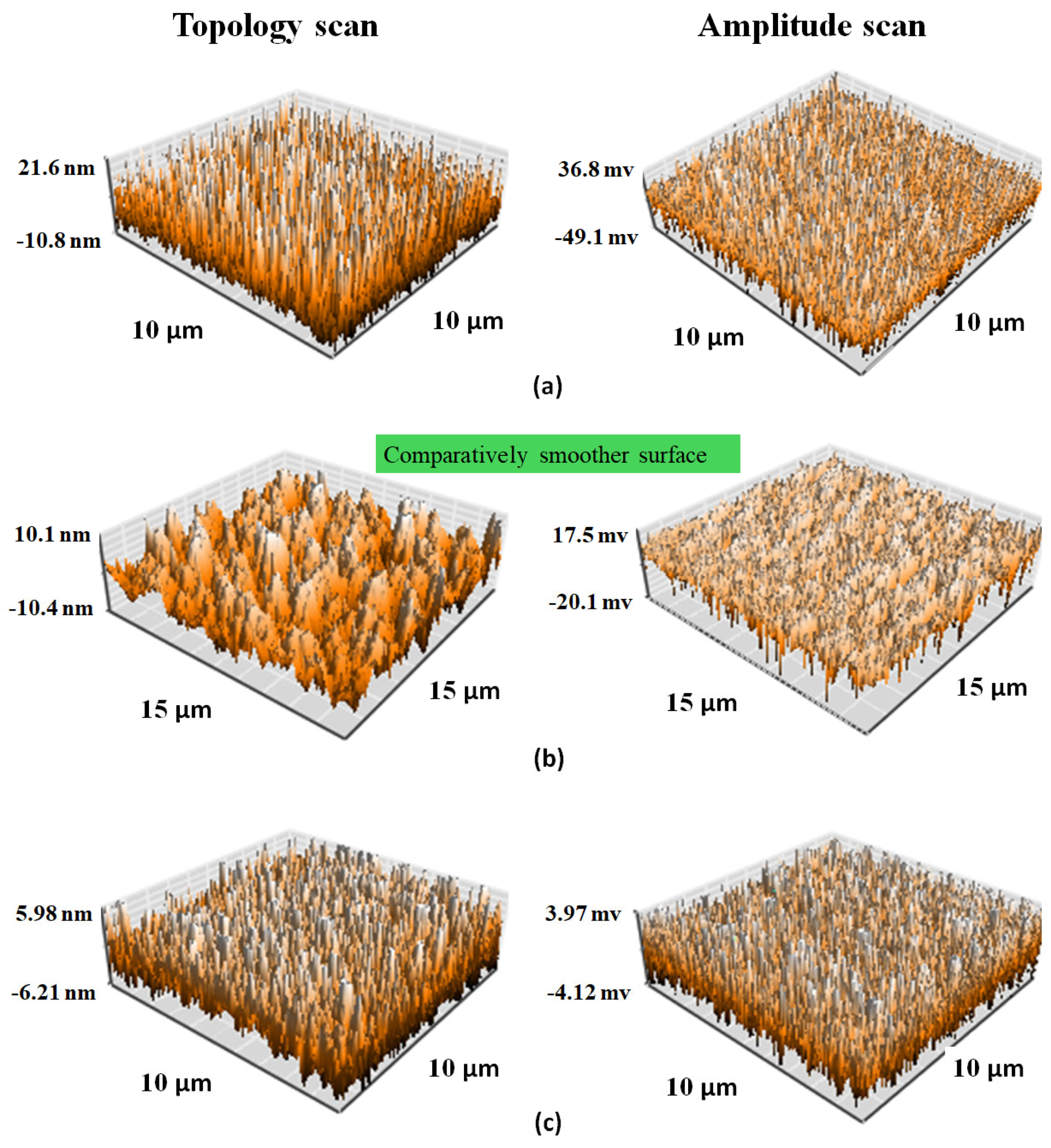
3.4. Mechanical/Structural Properties

Mechanical characteristics of ZnO–SiC composites are largely governed by their microstructural evolution, that is, by the influence of SiC reinforcement on the ZnO matrix. Experimentally, it was found that SiC particle addition enhances grain refinement and densification of the composite structure, leading to increased hardness, compressive strength, and wear resistance [74,75]. Duan et al., have also reported ZnO nanoparticles as being successfully anchored onto SiC surfaces, leading to improved interfacial compatibility and load transfer, which synergistically improve the structural integrity of the composite [59].
Previous experimental work reported on the achievement of improved micro-hardness and tribological stability with increased SiC content in ZnO-based composites [76,77]. Tensile strength measurements in epoxy-based nanocomposites revealed a positive correlation with ZnO and SiC filler loading, which implies that particle dispersion and interfacial adhesion have significant roles in optimizing mechanical performance. The microstructure analyses showed that the crystallinity and surface roughness of ZnO/SiC films are greatly influenced by deposition process parameters, and post-fabrication annealing treatments. Improved crystallinity and smoother surfaces can be achieved with optimized processing parameters reported in Ref [31]. Figure 6 displays the surface morphology of ZnO/SiC films fabricated by RF sputtering under varying sputtering power on the SiC target. Figure 6a is an example of high surface roughness where both topology and amplitude images have very tall and pointed peaks. These types of rough surfaces can potentially cause points of stress concentration that can negatively impact the material’s mechanical integrity under applied mechanical loading by nucleating microcracks. However, for some composite systems, this degree of roughness may also increase the mechanical interlocking between the filler and matrix and slightly improve adhesion. Figure 6b shows a roughly but more homogeneously distributed morphology, and the amplitude picture is said to possess a comparatively smoother surface. This smoother surface can result in better nanoparticle dispersion and stress distribution more homogeneously under load, exhibiting better tensile and impact toughness. A level topography has no defects and enhances bonding on the matrix–filler interface, which maximally improves higher mechanical properties. Figure 6c represents relatively low-amplitude and densely packed topographical features, which are indicative of fine-grained compact texture. Such features represent good interfacial contact and low porosity, both of which are beneficial for mechanical strengthening. The smoother and more homogeneous surface leads to effective load transfer mechanisms between reinforcement and matrix materials and therefore improved mechanical properties like hardness, compressive strength, and wear resistance. Such microstructural characteristics not only contribute to mechanical strengthening but also contribute to multifunctional capabilities such as thermal and electromagnetic shielding properties [59]. The smoother morphology is expected to reduce scattering centers and grain boundaries, which can positively impact carrier mobility in device applications. The observed differences likely arise from changes in plasma density and target composition, which influence adatom mobility and surface reorganization during film growth
An optimized and compact grain structure with reduced porosity and enhanced particle packing is typically observed in well-engineered ZnO–SiC systems. The high hardness and wear resistance of SiC improve the mechanical durability of ZnO/SiC composites, making them suitable for protective coatings and structural components. However, challenges such as homogeneous dispersion of nanoparticles and interfacial stress concentration must be well managed during synthesis to achieve the potential mechanical benefits of ZnO–SiC composites.

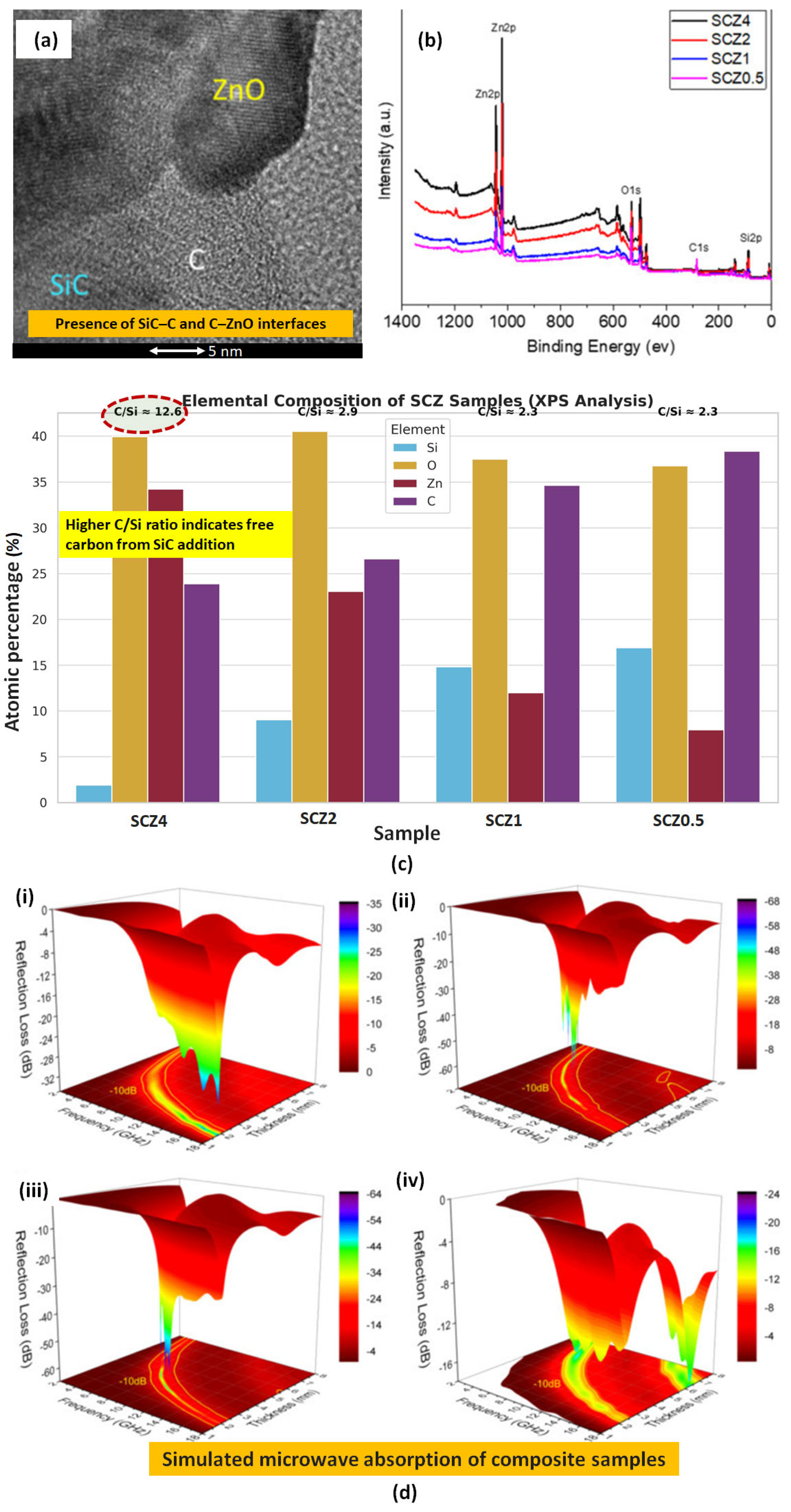
3.5. Interfacial Properties

The interfacial properties of ZnO–SiC composites are instrumental in establishing their mechanical strength and functional performance in a range of high-end applications. Incorporation of ZnO, particularly in nanostructured morphologies such as nanowires, can significantly enhance interfacial shear strength, up to 113%, without compromising the structural integrity of reinforcing fibers. This increased interface bonding directly translates to higher lamina shear strength and modulus, both of which have been observed to increase by 37.8% and 38.8%, respectively [78]. ZnO/SiC composite materials exhibit desirable characteristics for electron transport layers (ETLs) that include tunable n-type conductivity, optimized carrier concentration of 2.5–3.9 × 1014 cm3, and quite low resistivity (~5000 Ω·cm), as confirmed by Hall effect measurements. The composites also exhibit planar surface morphology and improved structural quality by incorporation of SiC, which causes improved interface contact with absorber layers, such as perovskite. For photovoltaic applications in ETL, the materials must be of proper band alignment, low surface roughness, high electron mobility, and low recombination losses. ZnO/SiC thin films meet most of these conditions and are therefore good candidates for high-efficiency solar cell integration.
In addition, their wide bandgap of 3.3–3.8 eV is beneficial for efficient charge transfer and high dielectric stability. Apart from structural and electronic benefits, ZnO-decorated SiC composites also have good electromagnetic absorption behavior, which exhibits even reflection loss of −65.4 dB at 11 GHz and hence finds its applicability in shielding [59]. Figure 7 presents the multifunctional enhancement enabled by the ZnO–SiC interfacial properties (structural, compositional, mechanical, and electromagnetic responsiveness). Despite these promising characteristics, optimizing processing routes and achieving homogeneous nanoparticle dispersion are the most important issues to be addressed to make the best use of ZnO–SiC composite potential in industrial applications. The high-resolution transmission electron microscopy (TEM) image uncovers the existence of two separate types of interfaces: one that exists between the SiC core and the carbon shell (SiC–C), and another that is situated between the carbon phase and the ZnO particles (C–ZnO) (Figure 7a). These interfacial configurations are anticipated to promote augmented interfacial polarization and multi-phase scattering, which significantly contribute to dielectric loss. Figure 7b showcases the X-ray photoelectron spectroscopy (XPS) profiles of the SCZ composite samples, wherein characteristic peaks corresponding to Zn 2p, O 1s, C 1s, and Si 2p are detected. The atomic ratios (Figure 7c) reveal a markedly higher C/Si ratio in the composites. This elevated ratio implies the presence of free carbon, likely derived from the incorporation of SiC, which is instrumental in modifying the electromagnetic characteristics of the material. The mechanical performance data depicted in Figure 7d illustrates the simulated microwave absorption behavior of the composite layers, where substantial reflection loss (RL) values below −10 dB are recorded across a range of frequencies and absorber thicknesses. Certain samples attain RL values below −50 dB, pointing out the potential of these composites for high-performance electromagnetic interference (EMI) shielding or stealth applications. These findings substantiate the multifunctional attributes of the ZnO–SiC composites, achieved through interface engineering and compositional optimization.

4. Application Perspectives

The unique combination of semiconducting, mechanical, and electromagnetic properties of ZnO/SiC composites makes them attractive for various applications in diverse fields such as microwave absorbers, electromagnetic interference (EMI) shielding materials, photocatalysts, and high-temperature structural components.

4.1. Photocatalysis

The photocatalytic capabilities of ZnO are preserved or even enhanced when coupled with SiC, extending the utility of the materials to water purification and environmental remediation. ZnO–SiC nanocomposites have been explored for photocatalytic applications in environmental remediation, especially in the breakdown of organic contaminants such as methylene blue, rhodamine B, and phenol under both ultraviolet and visible light exposure. The enhancement in photocatalytic efficiency (photocatalytic activity of ZnO–SiC nanocomposites under both UV and visible light irradiation is comprehensively illustrated in Figure 8) is largely due to the improved charge separation occurring at the ZnO–SiC interface, which mitigates the recombination of electron–hole pairs, a significant drawback in isolated ZnO photocatalysts. The heterojunction established between ZnO (a wide-bandgap n-type semiconductor) and SiC (a semiconductor characterized by high thermal conductivity and chemical inertness) promotes the effective transfer of photoexcited electrons from the conduction band of ZnO to that of SiC. This interfacial charge transfer mechanism extends the lifespan of charge carriers, thus facilitating greater involvement in redox reactions.
Moreover, the emergence of oxygen vacancies and surface defects at the ZnO–SiC interface enhances the adsorption capabilities of molecular oxygen and water, resulting in an increased production of reactive oxygen species (ROS) such as hydroxyl (OH) and superoxide (O2) radicals. These ROS are predominantly accountable for the oxidative degradation of organic pollutants. The inclusion of SiC further enhances the thermal stability, reusability, and mechanical integrity of the photocatalyst, which are essential for practical, long-term applications. Additionally, manipulating the morphology and particle dimensions of the composites, such as the development of core–shell or hierarchical nanostructures, can further improve light absorption, augment the active surface area, and elevate overall photocatalytic performance [32,79,80].
Consequently, ZnO–SiC composites signify a promising category of hybrid materials for sustainable photocatalytic technologies, presenting advantages in functionality, longevity, and recyclability.

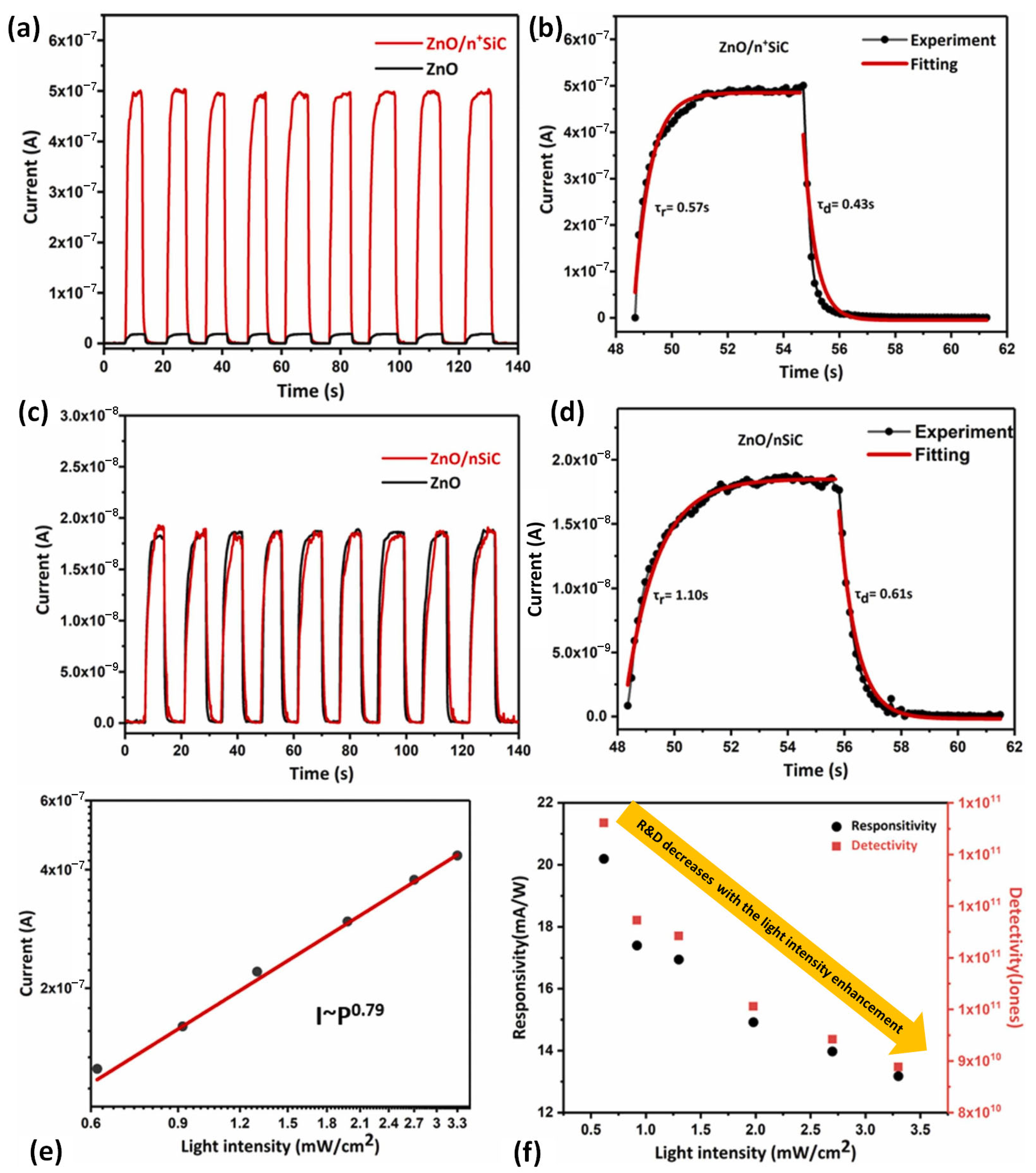
4.2. Optoelectronic Devices

ZnO/SiC composites are progressively being acknowledged for their remarkable optical transparency and broad bandgap properties, rendering them exceptionally appropriate for optoelectronic applications including light-emitting diodes (LEDs), photodetectors, and laser diodes. Notably, ZnO–SiC heterostructures have been thoroughly investigated for ultraviolet (UV) photodetection owing to their elevated detectivity, minimal dark current, and exceptional UV–Vis rejection ratios. These heterojunctions facilitate the efficient separation and transportation of charge carriers, thereby significantly bolstering photocurrent generation when subjected to UV light. For example, ZnO–a-SiC heterostructures have exhibited a responsivity of 37 mA/W alongside a dark current as low as 10 pA, indicating outstanding photoresponse and low-noise functionality [81]. Similarly, ZnO–4H-SiC heterojunctions with optimized doping configurations demonstrate improved optoelectronic performance, primarily attributed to enhanced carrier mobility and superior interface quality [82]. Furthermore, dark noise—one of the pivotal obstacles in photodetectors—is effectively alleviated through meticulous heterojunction design and interface engineering. Post-annealing processes further refine the interfacial characteristics, resulting in diminished trap states, reduced recombination, and improved operational stability of the devices [82,83]. Figure 9 illustrates the photodetection performance of ZnO–n-SiC heterojunctions compared to pristine ZnO. Figure 9a,c show that the ZnO/SiC device exhibits a significantly higher photocurrent and faster photoresponse under periodic illumination, indicating enhanced charge transport. Transient photoresponse fitting (Figure 9b,d) shows rise and decay times as low as 0.57 s and 0.43 s, respectively, superior to those of the pristine ZnO device. The power-dependent analysis reveals a sublinear relationship between photocurrent and light intensity (I ∝ P0.79), suggesting trap-assisted recombination. Notably, the responsivity and detectivity metrics decrease with higher light intensity but remain in the high-performance range, underscoring the potential of ZnO/SiC composites in visible-light photodetectors (Figure 9e,f). These results confirm the superior photoresponse characteristics of ZnO/SiC composites, attributed to efficient interfacial charge transfer and reduced recombination losses.

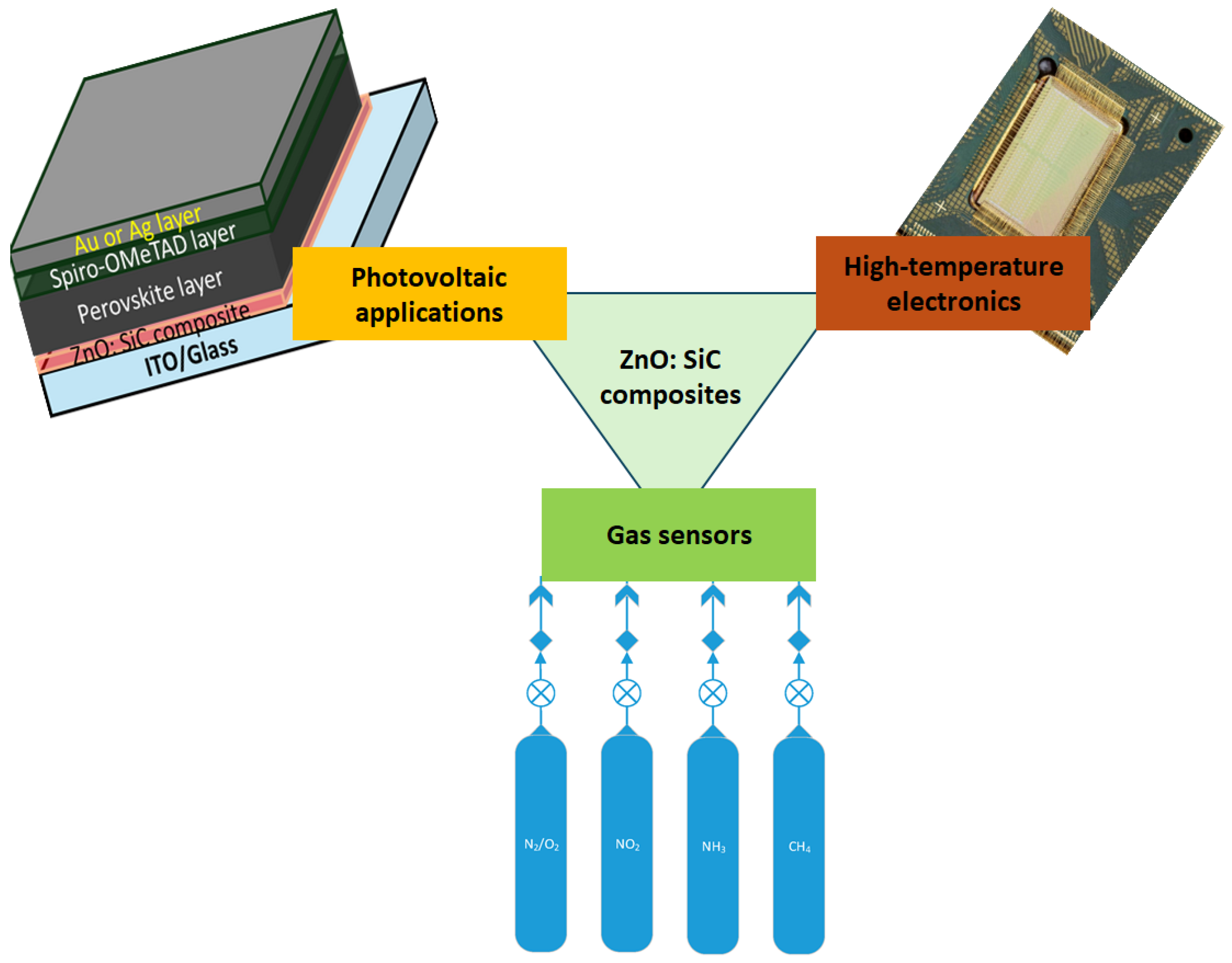
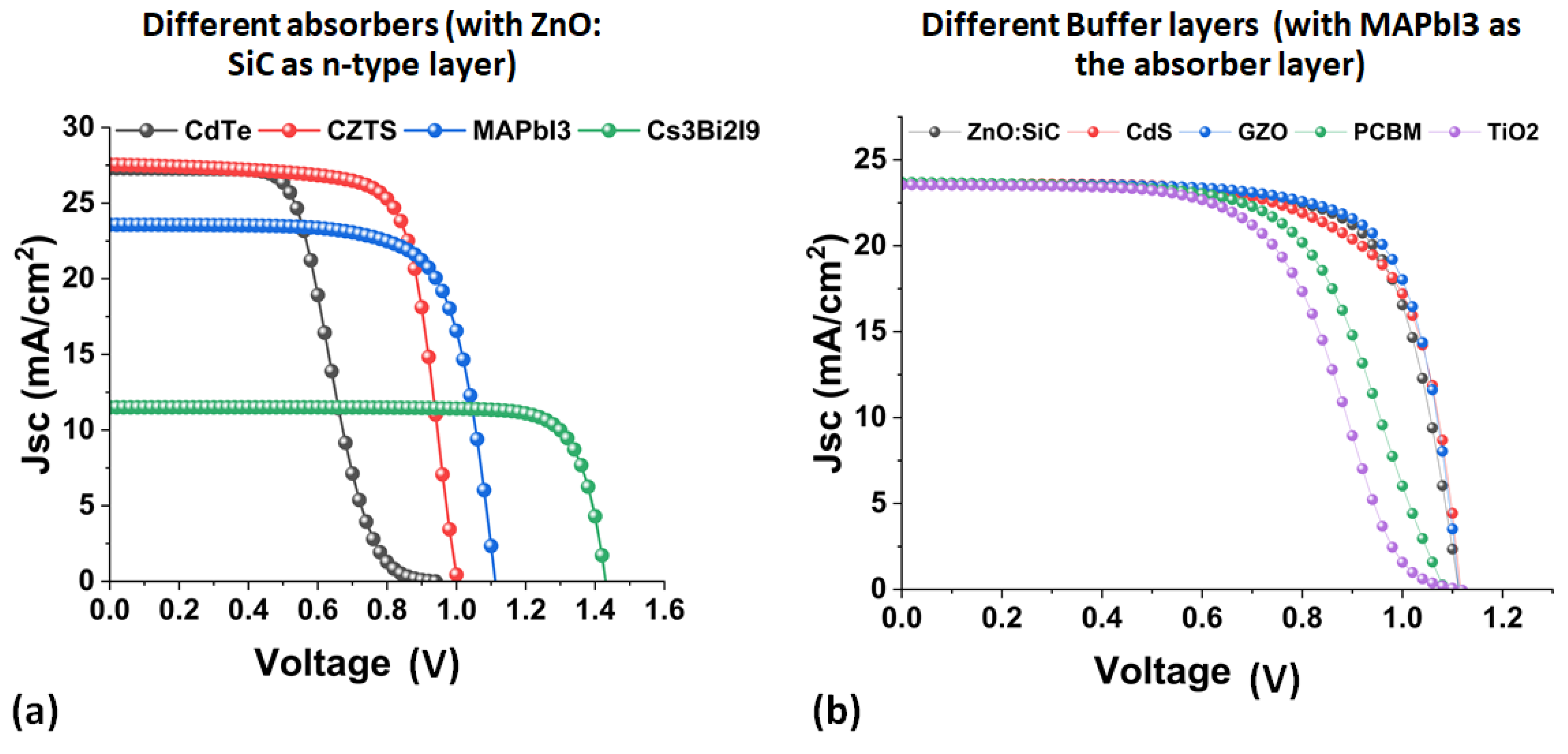
4.3. Potential Applications in Photovoltaics, High-Temperature Electronics, and Sensing Technologies

ZnO/SiC composites and heterostructures hold promising potential suitable to be applied across several high-impact domains, including photovoltaic energy conversion, high-temperature electronics, and gas sensing technologies (shown in Figure 10). Although direct applications are still under active exploration, their multifunctionality makes them attractive candidates for these technologically crucial areas.
ZnO/SiC-based heterostructures can be advantageous for next-generation photovoltaic (PV) devices. ZnO itself is a well-known wide bandgap semiconductor (∼3.37 eV) with strong UV absorption and high electron mobility, while SiC (especially 4H- or 6H-SiC) provides a complementary wide bandgap (∼3.2–3.3 eV), exceptional thermal conductivity, and chemical inertness. The combination of these materials can yield heterojunctions with enhanced charge carrier separation, suppressed recombination, and improved UV photoresponse, thereby boosting power conversion efficiency under broad-spectrum illumination. ZnO–4H-SiC heterojunctions show enhanced optoelectronic behavior, with improved photocurrent generation and reduced dark current, especially after post-deposition annealing treatments that optimize interfacial quality [81,82]. This nature indicates that this composite material could be a promising candidate for the integration into thin-film-based solar cells, UV-enhanced photovoltaic modules, or as transparent electrodes or buffer layers in tandem solar cell architectures, which is also confirmed by a preliminary simulation exploration. The observed light absorption enhancement and the reduction in carrier recombination could improve power conversion efficiencies in next-generation photovoltaic devices. In addition, the integration of SiC into ZnO matrices enhances charge transfer efficiency and reduces surface roughness, which is essential for the development of any opto-electrical micro/nano-devices. To evaluate the potential of ZnO/SiC composites for photovoltaic devices, simulations at the device level were carried out with various absorber materials with ZnO/SiC as the electron transport layer (ETL). As is apparent from Figure 11a, ZnO/SiC enabled robust performance with both wide-bandgap and narrow-bandgap absorbers, with MAPbI3 and CZTS recording particularly high Jsc and Voc. Comparison to other conventional buffer layers (Figure 11b) in MAPbI3-based devices revealed that ZnO/SiC offers comparable or superior current extraction, solidifying its great potential as a multifunctional ETL for upcoming perovskite and inorganic solar cells. Simulation of perovskite solar cells incorporating ZnO/SiC as either the electron transport or buffer layer revealed promising device characteristics with short-circuit current density (Jsc) exceeding 24 mA/cm2 and open-circuit voltage (Voc) up to 1.2 V. The relative power conversion efficiency reached ~18.5%, validating the potential of ZnO/SiC for next-generation optoelectronics.
On the other hand, the chemical stability of SiC can enhance thermal and electrical stability, which makes it a preferred material in high-power and high-temperature electronics. This type of composite can impart additional functional properties such as sensitive optoelectronic response, piezoelectricity, and photoconductivity, expanding their application range. ZnO–SiC heterostructures have already been explored for UV photodetectors that operate stably at elevated temperatures, with high responsivity and fast response times. These characteristics align well with the requirements of aerospace, automotive, and industrial control systems, where materials must withstand temperatures exceeding 300 °C and operate under fluctuating thermal loads. Finally, ZnO/SiC composites or heterostructures could play a transformative role in developing radiation-hardened circuits, high-frequency transistors, and smart sensors for extreme environments.
Furthermore, while direct studies specifically using ZnO/SiC composites for gas sensing are yet to be developed, the well-established sensing capabilities of the individual components ZnO and SiC provide a strong foundation for future exploration. ZnO is widely used as a gas-sensitive material for detecting NO2, CO, H2S, ethanol, and volatile organic compounds due to its high surface area and surface reactivity. On the other hand, SiC, especially in amorphous and nanoform, has been reported to enhance selectivity and sensing stability at elevated temperatures, owing to its chemical robustness and active functional surface groups. Several studies have demonstrated that ZnO/SiC composites significantly outperform pristine ZnO in device-level performance, particularly in UV photodetectors and gas sensors. For instance, ZnO–SiC heterojunctions exhibit higher responsivity (up to 1.29 mA/W at 365 nm), faster response times (11.4 ms rise and 14.2 ms decay), and lower dark currents compared to undoped ZnO devices [67,81,82]. In gas sensing, ZnO/SiC-based sensors have shown enhanced sensitivity (up to 90% for NO2 at 100 ppm) and lower detection limits (as low as 100 ppb), attributed to the improved surface reactivity and electron transport properties introduced by SiC [33,68].
Integrating ZnO with SiC in composite or heterostructured formats could potentially combine the high sensitivity of ZnO with the selectivity, stability, and durability of SiC. This would be particularly useful in developing next-generation sensors for real-time detection of hazardous gases in high-temperature environments such as combustion exhaust systems, industrial plants, and underground mines. Future studies could investigate how the interface properties, defect states, and surface chemistry of ZnO/SiC composites can be engineered to optimize gas adsorption and electron transport mechanisms.

5. Challenges and Future Perspectives

Despite their promising applications, ZnO/SiC composites face several challenges, including the following:
  • Synthesis Complexity: achieving uniform dispersion and phase compatibility remains a challenge.
  • Cost of Production: advanced synthesis methods like CVD are expensive and may limit large-scale production.
  • Stability Issues: long-term stability under operational conditions needs further research.
Future research should focus on optimizing synthesis techniques, exploring novel doping strategies, and developing scalable fabrication methods to enhance the performance and cost-effectiveness of ZnO/SiC composites.

6. Conclusions

ZnO/SiC composite materials are found to exhibit better material properties, which make them extremely suitable for a wide range of applications, from photo-catalysis and optoelectronics to gas sensing and solar cells. The optical properties of the composite will depend on the relative amounts of ZnO and SiC, along with the homogeneity of blending. Given an optimized mixture, the composite may have the optical transparency properties of the two materials. However, if the mixing is non-homogeneous, optical scattering at the ZnO–SiC phase boundaries can occur, which may reduce transparency. The electrical characteristics of the composite will be a function of the relative ZnO and SiC concentrations. The addition of ZnO to SiC may alter the conductivity and other electrical characteristics of the composite, depending on the volume fraction and dispersion of the individual phases. This review highlights synthesis techniques, main properties, and application perspectives of ZnO/SiC composites and discusses the prospects and challenges in this field. The integration of SiC with ZnO provides synergistic benefits such as improved carrier mobility, enhanced surface activity, and increased environmental stability. Experimental photodetector results indicate fast rise and decay times with excellent linearity across varying light intensities, validating their potential for photoactive device integration. Despite the evident potential, several challenges and research gaps remain, such as a lack of direct application evidence on photovoltaic devices or commercial sensors. Future research should fabricate and test real devices under practical conditions, with the additional techno-economic analyses and optimized fabrication pathways for industrial and commercial advancements.

Funding

This research received no external funding.

Data Availability Statement

No new data were created or analyzed in this study. Data sharing does not apply to this article.

Acknowledgments

The author would like to acknowledge the academic support given by Edith Cowan University, Australia, Universiti Tenaga Nasional, Malaysia, and Graphic Era University, India.

Conflicts of Interest

The author declares no conflicts of interest.

References

  1. Cuadra, J.G.; Estrada, A.C.; Oliveira, C.; Abderrahim, L.A.; Porcar, S.; Fraga, D.; Trindade, T.; Seabra, M.P.; Labrincha, J.; Carda, J.B. Functional properties of transparent ZnO thin films synthesized by using spray pyrolysis for environmental and biomedical applications. Ceram. Int. 2023, 49, 32779–32788. [Google Scholar] [CrossRef]
  2. Kumar, V.; Prakash, J.; Pathak, D.; Sharma, D.P.; Purohit, L.P.; Swart, H.C. Ion beam engineering of implanted ZnO thin films for solar cell and lighting applications. Chem. Eng. J. Adv. 2023, 15, 100501. [Google Scholar] [CrossRef]
  3. Petrov, V.V.; Sysoev, V.V.; Ignatieva, I.O.; Gulyaeva, I.A.; Volkova, M.G.; Ivanishcheva, A.P.; Khubezhov, S.A.; Varzarev, Y.N.; Bayan, E.M. Nanocomposite Co3O4-ZnO Thin Films for Photoconductivity Sensors. Sensors 2023, 23, 5617. [Google Scholar] [CrossRef] [PubMed]
  4. Krysova, H.; Mansfeldova, V.; Tarabkova, H.; Pisarikova, A.; Hubicka, Z.; Kavan, L. High-quality dense ZnO thin films: Work function and photo/electrochemical properties. J. Solid State Electrochem. 2024, 28, 2531–2546. [Google Scholar] [CrossRef]
  5. Gartner, M.; Stroescu, H.; Mitrea, D.; Nicolescu, M. Various Applications of ZnO Thin Films Obtained by Chemical Routes in the Last Decade. Molecules 2023, 28, 4674. [Google Scholar] [CrossRef]
  6. Toma, M.; Domokos, R.; Lung, C.; Marconi, D.; Pop, M. Characterization of ZnO, Ga-Doped ZnO, and Nd-Ga-Doped ZnO Thin Films Synthesized by Radiofrequency Magnetron Sputtering. Anal. Lett. 2023, 57, 797–811. [Google Scholar] [CrossRef]
  7. Petrov, V.V.; Ignatieva, I.O.; Volkova, M.G.; Gulyaeva, I.A.; Pankov, I.V.; Bayan, E.M. Polycrystalline Transparent Al-Doped ZnO Thin Films for Photosensitivity and Optoelectronic Applications. Nanomaterials 2023, 13, 2348. [Google Scholar] [CrossRef]
  8. Uzar, N.; Abdulaziz, U.; Erbas, O.G.; Aydin, M.; Dolgun, M.F. Enhancement of structural, optical, electrical, optoelectronic and thermoelectric properties of ZnO thin film via Ni doping and Ni-B co-doping. Phys. Scr. 2024, 99, 075995. [Google Scholar] [CrossRef]
  9. Nur-E-Alam, M.; Ferdaous, M.T.; Alghafis, A.; Vasiliev, M.; Yap, B.K.; Kiong, T.S.; Sapeli, M.M.I.; Amin, N.; Ibrahim, M.A.; Bin Rafiq, M.K.S. Tailoring Ga-Doped ZnO Thin Film Properties for Enhanced Optoelectric Device Performance: Argon Flow Rate Modulation and Dynamic Sputtering Geometry Analysis. Sol. RRL 2025, 9, 2400353. [Google Scholar] [CrossRef]
  10. Al-Maamori, M.H.; Al-Jamal, A.N.; Habeeb, S.A.; Hassan, A.S.; Majdi, H.S. Al3+-modified ZnO thin film sensor fabricated by the sputtering method: Characterization and a carbon monoxide gas detection study. J. Chem. Res. 2024, 48, 17475198231221453. [Google Scholar] [CrossRef]
  11. Sharma, H.; Kumar, S.; Yadav, J.; Prasad, J.; Singh, M. Effect of Sn-incorporation on the Structural and Optical Properties of ZnO Thin Films Prepared by Sol-Gel Method. Orient. J. Chem. 2023, 39, 1540–1546. [Google Scholar] [CrossRef]
  12. Vyas, S. A short review on properties of and applications of Zinc Oxide based thin films and devices. Johns. Matthey Technol. Rev. 2020, 64, 202–218. [Google Scholar] [CrossRef]
  13. Vagena, I.-A.; Gatou, M.-A.; Theocharous, G.; Pantelis, P.; Gazouli, M.; Pippa, N.; Gorgoulis, V.G.; Pavlatou, E.A.; Lagopati, N. Functionalized ZnO-Based Nanocomposites for Diverse Biological Applications: Current Trends and Future Perspectives. Nanomaterials 2024, 14, 397. [Google Scholar] [CrossRef] [PubMed]
  14. Oloruntoba, S.O.; Zainal, Z.; Sulaiman, Y.; Zawawi, R.M. Fabrication of Zinc Oxide thin films by Sol-Gel dip coating process. J. Nanosci. Res. Rep. 2024, 6, 1–6. [Google Scholar] [CrossRef]
  15. Gonzalez Cuadra, J.; Lahlahi, A.; Porcar, S.; Cadena, R.; Toca, S.; Fraga, D.; Carda, J. Zinc Oxide Thin Films: Synthesis and Photocatalytic Applications; IntechOpen: London, UK, 2024. [Google Scholar] [CrossRef]
  16. Dawka, S.; Duan, P.; Maitra, S.; Sapkota, R.; Papadopoulos, C. Solution-Processed Zinc Oxide Nanoparticles for Thin Film Optoelectronic Neuromorphic Devices. Meet. Abstr. 2024, MA2024-02, 2531. [Google Scholar] [CrossRef]
  17. Clancy, M. How Silicon Carbide Thin Films Are Revolutionizing Power Electronics. Available online: https://korvustech.com/silicon-carbide-thin-films/ (accessed on 4 March 2025).
  18. Chaussende, D.; Tabouret, V.; Crisci, A.; Morais, M.; Coindeau, S.; Berthomé, G.; Kollmuss, M.; Wellmann, P.; Jomard, F.; Pinault-Thaury, M.-A.; et al. Investigation of amorphous-SiC thin film deposition by RF magnetron sputtering for optical applications. Mater. Sci. Semicond. Process. 2024, 182, 108673. [Google Scholar] [CrossRef]
  19. Xu, M.; Shin, D.; Sberna, P.M.; van der Kolk, R.; Cupertino, A.; Bessa, M.A.; Norte, R.A. High-Strength Amorphous Silicon Carbide for Nanomechanics. Adv. Mater. 2024, 36, 2306513. [Google Scholar] [CrossRef]
  20. Kaloyeros, A.E.; Arkles, B. Silicon Carbide Thin Film Technologies: Recent Advances in Processing, Properties, and Applications—Part I Thermal and Plasma CVD. ECS J. Solid State Sci. Technol. 2023, 12, 103001. [Google Scholar] [CrossRef]
  21. Lopez-Rodriguez, B.; van der Kolk, R.; Aggarwal, S.; Naresh, S.; Li, Z.; van der Plaats, D.; Scholte, T.; Chang, J.; Gröblacher, S.; Pereira, S.F.; et al. High-Quality Amorphous Silicon carbide for hybrid photonic integration deposited at a low temperature. ACS Photonics 2023, 10, 3748–3754. [Google Scholar] [CrossRef]
  22. Greenhorn, S.; Bano, E.; Stambouli, V.; Zekentes, K. Amorphous SiC Thin Films Deposited by Plasma-Enhanced Chemical Vapor Deposition for Passivation in Biomedical Devices. Materials 2024, 17, 1135. [Google Scholar] [CrossRef]
  23. Krupa, M.M. Silicon carbide films as protective and optical coatings. Int. J. Chem. Eng. Mater. 2024, 3, 55–58. [Google Scholar] [CrossRef]
  24. Shah, A. Chapter IC-1—Thin-Film Silicon Solar Cells1. In Solar Cells, 2nd ed.; McEvoy, A., Castañer, L., Markvart, T., Eds.; Elsevier: Amsterdam, The Netherlands, 2013; pp. 159–223. ISBN 9780123869647. [Google Scholar] [CrossRef]
  25. EKaloyeros, A.; Arkles, B. Silicon Carbide Thin Films: Innovations in Property, Process, and Applications; IntechOpen: London, UK, 2025. [Google Scholar] [CrossRef]
  26. Trzepieciński, T.; Batu, T.; Kibrete, F.; Lemu, H.G. Application of Composite Materials for Energy Generation Devices. J. Compos. Sci. 2023, 7, 55. [Google Scholar] [CrossRef]
  27. Ince, J.C.; Peerzada, M.; Mathews, L.D.; Pai, A.R.; Al-qatatsheh, A.; Abbasi, S.; Yin, Y.; Hameed, N.; Duffy, A.R.; Lau, A.K.; et al. Overview of emerging hybrid and composite materials for space applications. Adv. Compos. Hybrid Mater. 2023, 6, 130. [Google Scholar] [CrossRef]
  28. Nur-E-Alam, M.; Basher, M.K.; Vasiliev, M.; Das, N. Physical Vapor-Deposited Silver (Ag)-Based Metal-Dielectric Nanocomposites for Thin-Film and Coating Applications. Appl. Sci. 2021, 11, 6746. [Google Scholar] [CrossRef]
  29. Nur-E-Alam, M.; Yap, B.K.; Basher, M.K.; Islam, M.A.; Hossain, M.K.; Soudagar, M.E.M.; Das, N.; Vasiliev, M.; Kiong, T.S. Multifunctional Prospects of Physical Vapor-Deposited Silver-Based Metal-Dielectric Nanocomposite Thin Films. J. Sci. Adv. Mater. Devices 2025, 10, 100871. [Google Scholar] [CrossRef]
  30. El-Fattah, H.A. Effect of surface morphology on optical properties of two multilayer structures CuO/ZnO/SiC and Al2O3/ZnO/SiC. Sci. Rep. 2023, 13, 23035. [Google Scholar] [CrossRef]
  31. Mosabbir, A.S.M.; Sadek, M.S.; Mahmood, M.; Sultan, S.M.; Alshammari, F.; Alobaid, M.; Alghafis, A.A.; Ibrahim, M.A.; Sobayel, K. Exploration of ZnO:SiC composite material for photovoltaic applications. Interactions 2025, 246, 7. [Google Scholar] [CrossRef]
  32. GMeenakshi, A. Sivasamy, Nanorod ZnO/SiC nanocomposite: An efficient catalyst for the degradation of an endocrine disruptor under UV and visible light irradiations. J. Environ. Chem. Eng. 2018, 6, 3757–3769. [Google Scholar] [CrossRef]
  33. Zhang, J.; Cui, Y.; Lin, Y.; Tang, Y.; Yu, Y.; Yan, S.; Gao, B.; Hu, G.; Chu, P.K. Facile fabrication of SiC/ZnO composite and its enhanced sensitivity for detection of NO. AIP Adv. 2023, 13, 105218. [Google Scholar] [CrossRef]
  34. Bokov, D.; Turki Jalil, A.; Chupradit, S.; Suksatan, W.; Javed Ansari, M.; Shewael, I.H.; Valiev, G.H.; Kianfar, E. Nanomaterial by Sol-Gel Method: Synthesis and Applicatio. Adv. Mater. Sci. Eng. 2021, 2021, 5102014. [Google Scholar] [CrossRef]
  35. Potter, D.B.; Powell, M.J.; Darr, J.A.; Parkin, I.P.; Carmalt, C.J. Transparent conducting oxide thin films of Si-doped ZnO prepared by aerosol assisted CVD. RSC Adv. 2017, 7, 10806–10814. [Google Scholar] [CrossRef]
  36. Nakano, T.; Tanehira, T.; Ishitani, K.; Nakao, M. Growth of ZnO Epitaxial Films Using 3C-SiC Substrate with Buried Insulating Layer. Jpn. J. Appl. Phys. 2009, 48, 041106. [Google Scholar] [CrossRef]
  37. Ashrafi, A.B.M.A.; Zhang, B.-P.; Binh, N.T.; Wakatsuki, K.; Segawa, Y. High-Quality ZnO Layers Grown on 6H-SiC Substrates by Metalorganic Chemical Vapor Deposition. Jpn. J. Appl. Phys. 2004, 43, 1114. [Google Scholar] [CrossRef]
  38. Shtepliuk, I.; Khranovskyy, V.; Ievtushenko, A.; Yakimova, R. Temperature-Dependent Photoluminescence of ZnO Thin Films Grown on Off-Axis SiC Substrates by APMOCVD. Materials 2021, 14, 1035. [Google Scholar] [CrossRef]
  39. Lim, T. Nanoengineering of ZnO Electrical and Optical Characteristics by Controlling Its Morphology and Defects via Reaction Kinetics, Fluid Dynamics, and Stoichiometry in Low-Pressure CVD Synthesis. Ph.D. Thesis, University of California, Riverside, CA, USA, 2016. Available online: https://escholarship.org/uc/item/9s12n1kf (accessed on 28 April 2025).
  40. Bekermann, D.; Gasparotto, A.; Barreca, D.; Bovo, L.; Devi, A.; Fischer, R.A.; Lebedev, O.I.; Maccato, C.; Tondello, E.; Tendeloo, G.V. Highly Oriented ZnO Nanorod Arrays by a Novel Plasma Chemical Vapor Deposition Process. Cryst. Growth Des. 2010, 10, 2011–2018. [Google Scholar] [CrossRef]
  41. Sánchez-Martín, S.; Olaizola, S.M.; Castaño, E.; Urionabarrenetxea, E.; Mandayo, G.G.; Ayerdi, I. Study of deposition parameters and growth kinetics of ZnO deposited by aerosol assisted chemical vapor deposition. RSC Adv. 2021, 11, 18493–18499. [Google Scholar] [CrossRef]
  42. Ahmmad, B.; Kanomata, K.; Hirose, F. Controlled Morphologies of Nanostructured ZnO Films by MOCVD Method. Appl. Mech. Mater. 2014, 492, 311–315. [Google Scholar] [CrossRef]
  43. Sabzi, M.; Mousavi Anijdan, S.H.; Shamsodin, M.; Farzam, M.; Hojjati-Najafabadi, A.; Feng, P.; Park, N.; Lee, U. A Review on Sustainable Manufacturing of Ceramic-Based Thin Films by Chemical Vapor Deposition (CVD): Reactions Kinetics and the Deposition Mechanisms. Coatings 2023, 13, 188. [Google Scholar] [CrossRef]
  44. Cao, K.; Li, H.; Xia, S.; Liu, H.; Yang, T.; Zheng, Y.; Wang, J.; Zhang, B.; Li, H. A batch preparation of large-size graphite plate/SiC coating by CVD: CFD simulation and experimental. Ceram. Int. 2024, 50, 16798–16812. [Google Scholar] [CrossRef]
  45. Xu, J.; Tian, H.J.; Tian, Y.J.; Wen, H. Fabrication of Micro-Structural ZnO Crystal and the Concentration Fields of the CVD Reactor. Adv. Mater. Res. 2013, 750–752, 352–357. [Google Scholar] [CrossRef]
  46. Ali, W.A.; Richards, S.E.; Alzard, R.H. Unlocking the potential of ball milling for nanomaterial Synthesis: An overview. J. Ind. Eng. Chem. 2025, 149, 63–93. [Google Scholar] [CrossRef]
  47. Erdemir, F.; Varol, T. and Çanakçı, A. Synthesis of SiC nanoparticles by central composite design response surface methodology directed mechanical milling. Micro Nano Lett. 2020, 15, 187–190. [Google Scholar] [CrossRef]
  48. Jasim, A.H.; Joudi, W.M.; Radhi, N.S.; Saud, A.N. Mechanical properties and wear characteristics of (Aluminum-Zinc Oxide) metal matrix composite prepared using Stir casting process. Mater. Sci. Forum 2020, 1002, 175–184. [Google Scholar] [CrossRef]
  49. Arora, S.; Srivastava, C. Synthesis of ZnO Nanocrystal–Graphene Composite by Mechanical Milling and Sonication-Assisted Exfoliation. JOM 2017, 69, 1021–1026. [Google Scholar] [CrossRef]
  50. Abduev, A.K.; Akhmedov, A.K.; Asvarov, A.S.; Rabadanov, K.S.; Emirov, R.M. Formation of a ZnO–C Composite with a Nanocrystalline Structure. Tech. Phys. 2019, 64, 666–673. [Google Scholar] [CrossRef]
  51. Gençyılmaz, O. Hydrothermal synthesis of ZnO films and characterization. Anadolu Univ. J. Sci. Technol. A—Appl. Sci. Eng. 2016, 17, 660–669. [Google Scholar] [CrossRef]
  52. Lien, W.-C.; Tsai, D.-S.; Chiu, S.H.; Senesky, D.G.; Maboudian, R.; Pisano, A.P.; He, J.H. Low-Temperature, Ion Beam-Assisted SiC Thin Films with Antireflective ZnO Nanorod Arrays for High-Temperature Photodetection. IEEE Electron Device Lett. 2011, 32, 1564–1566. [Google Scholar] [CrossRef]
  53. Ma, H.C.; Yuan, S.Y.; Fu, Y.H.; Dong, X.L.; Zhang, X.F.; Ma, C.; Zhang, X.X. Hydrothermal Synthesis of ZnO/Zn Composites with Enhanced Photocatalytic Performance. Adv. Mater. Res. 2012, 518–523, 746–749. [Google Scholar] [CrossRef]
  54. Gupta, M.K.; Kumar, Y.; Sonnathi, N.; Sharma, S.K. Hydrothermally Grown Zinc Oxide Nanostructures@Carbon Composites for Supercapacitor Application. Phys. Status Solidi A 2023, 220, 2200451. [Google Scholar] [CrossRef]
  55. El-Shafey, H.M.; Saif, M.; Aly, M.H.; Hafez, H.S. Enhancing the Photo and Biomedical Activity of ZnO by Incorporation with Zinc Silicate Nanocomposites. Appl. Organomet. Chem. 2020, 34, e5902. [Google Scholar] [CrossRef]
  56. Felix, J.F.; Aziz, M.; de Araujo, C.I.L.; de Azevedo, W.M.; Anjos, V.; da Silva, E.F.; Henini, M. Zinc oxide thin films on silicon carbide substrates (ZnO/SiC): Electro-optical properties and electrically active defects. Semicond. Sci. Technol. 2014, 29, 045021. [Google Scholar] [CrossRef]
  57. Fu, Z. ZnO/SiC/Si Heterojunction Solar Battery and Preparation Method Thereof. 2012. Available online: https://patents.google.com/patent/CN101694853B/en (accessed on 29 April 2025).
  58. Daniel, A.; Belmonte, T. Synthesis of Si—Zn—O Composite Thin Films by a Hybrid PECVD-PVD Radiofrequency Process. Plasma Process. Polym. 2007, 4, S664–S667. [Google Scholar] [CrossRef]
  59. Duan, L.; Yang, Z.; Xia, Y.; Dai, X.; Wu, J.; Sun, M. ZnO-decorated SiC@C hybrids with strong electromagnetic absorption. Beilstein J. Nanotechnol. 2023, 14, 565–573. [Google Scholar] [CrossRef]
  60. Alam, M.N.-E.; Vasiliev, M.; Alameh, K. High-performance RF-sputtered Bi-substituted iron garnet thin films with almost in-plane magnetization. Opt. Mater. Express 2017, 7, 676–686. [Google Scholar] [CrossRef]
  61. Nur-E-Alam, M.; Vasiliev, M.; Alameh, K. Bi-Substituted Ferrite Garnet Type Magneto-Optic Materials Studied at ESRI Nano-Fabrication Laboratories, ECU, Australia. Coatings 2022, 12, 1471. [Google Scholar] [CrossRef]
  62. Choudhary, S.; Sharma, V.; Sharma, A.; Kumar, A.; Kumar, P. Analyzing the Properties of Zinc Oxide (ZnO) Thin Film Grown on Silicon (Si) Substrate, ZnO/Si Using RF Magnetron Sputtering Approach. In Modeling, Characterization, and Processing of Smart Materials; Kumar, A., Kumar, P., Srivastava, A., Goyat, V., Eds.; IGI Global Scientific Publishing: Hershey, PA, USA, 2023; pp. 297–308. [Google Scholar] [CrossRef]
  63. Li, Q.; Fu, S.; Song, C.; Wang, G.; Zeng, F.; Pan, F. Sputtering power dependence of structure and photoluminescence of ZnO on 6H–SiC. J. Mater. Sci. Mater. Electron. 2017, 28, 17881–17888. [Google Scholar] [CrossRef]
  64. Nomoto, J.-i.; Miyata, T.; Minami, T. Transparent conducting Si-codoped Al-doped ZnO thin films prepared by magnetron sputtering using Al-doped ZnO powder targets containing SiC. J. Vac. Sci. Technol. A 2009, 27, 1001–1005. [Google Scholar] [CrossRef]
  65. Al-Bataineh, Q.M.; Telfah, M.; Ahmad, A.A.; Alsaad, A.M.; Qattan, I.A.; Baaziz, H.; Charifi, Z.; Telfah, A. Synthesis, Crystallography, Microstructure, Crystal Defects, Optical and Optoelectronic Properties of ZnO:CeO2 Mixed Oxide Thin Films. Photonics 2020, 7, 112. [Google Scholar] [CrossRef]
  66. Taube, A.; Sochacki, M.; Kwietniewski, N.; Werbowy, A.; Gierałtowska, S.; Wachnicki, L.; Godlewski, M.; Szmidt, J. Electrical properties of isotype and anisotype ZnO/4H-SiC heterojunction diodes. Appl. Phys. Lett. 2017, 110, 143509. [Google Scholar] [CrossRef]
  67. Chen, Y.; Saraf, G.; Reyes, P.I.; Duan, Z.; Zhong, J.; Lu, Y. Structural, electrical, and piezoelectric properties of ZnO films on Si C-6 H substrates. J. Vac. Sci. Technol. B 2009, 27, 1631. [Google Scholar] [CrossRef]
  68. Alivov, Y.I.; Johnstone, D.; Özgür, U.; Avrutin, V.; Fan, Q.; Akarca-Biyikli, S.S.; Morkoç, H. Electrical and Optical Properties of n-ZnO/p-SiC Heterojunctions. Jpn. J. Appl. Phys. 2005, 44, 7281–7284. [Google Scholar] [CrossRef]
  69. Platonov, V.B.; Rumyantseva, M.N.; Frolov, A.S.; Yapryntsev, A.D.; Gaskov, A.M. High-temperature resistive gas sensors based on ZnO/SiC nanocomposites. Beilstein J. Nanotechnol. 2019, 10, 1537–1547. [Google Scholar] [CrossRef] [PubMed]
  70. Krishnasamy, E.; Iyyanar, S.; Munusamy, V.; Priya, S.D.; Fallah, M.H.; Singh, K. Study on the effect of ZnO nanoparticles embedded ramie fiber reinforced epoxy matrix composite—A novel material for sustainable development. E3S Web Conf. 2024, 588, 01017. [Google Scholar] [CrossRef]
  71. Raja, T.; Devarajan, Y.; Kailiappan, N. Study on enhancing mechanical and thermal properties of carbon fiber reinforced epoxy composite through zinc oxide nanofiller. Discov. Appl. Sci. 2024, 6, 566. [Google Scholar] [CrossRef]
  72. Badini, C.; Fino, P.; Ubertalli, G.; Taricco, F. Degradation at 1200 °C of a SiC coated 2D-Nicalon/C/SiC composite processed by SICFILL® method. J. Eur. Ceram. Soc. 2000, 20, 1505–1514. [Google Scholar] [CrossRef]
  73. Sun, M.; Lv, X.; Xie, A.; Jiang, W.; Wu, F. Growing 3D ZnO nano-crystals on 1D SiC nanowires: Enhancement of dielectric properties excellent electromagnetic absorption performance. J. Mater. Chem. C 2016, 4, 8897–8902. [Google Scholar] [CrossRef]
  74. Božić, D.; Devečerski, A.; Dimčić, B.; Vilotijević, M.; Rajković, V. Structural and mechanical characteristics of ZA27-7 wt.% SiC composites produced by powder metallurgy techniques. Int. J. Mater. Res. 2022, 95, 704–707. [Google Scholar] [CrossRef]
  75. Jin, X.H.; Gao, L.; Sun, J. Mechanical Performances of ZTM/SiC Nanocomposite Optimized through Composition and Microstructure Tailoring. Mater. Sci. Forum 2008, 569, 89–92. [Google Scholar] [CrossRef]
  76. Dass, K.; Chauhan, S.R.; Gaur, B. Study on the effects of nanoparticulates of SiC, Al2O3, and ZnO on the mechanical and tribological performance of epoxy-based nanocomposites. Part. Sci. Technol. 2016, 35, 589–606. [Google Scholar] [CrossRef]
  77. Fayomi, O.S.I.; Popoola, A.P.I.; Oheiza, A.; Adekeye, T. Microstructure, tribological and mechanical strengthening effect of multiphase Zn/ZrO2-SiC electrodeposited composite coatings. Int. J. Adv. Manuf. Technol. 2015, 80, 1489–1495. [Google Scholar] [CrossRef]
  78. Lin, Y.; Ehlert, G.; Sodano, H.A. Increased Interface Strength in Carbon Fiber Composites through a ZnO Nanowire Interphase. Adv. Funct. Mater. 2009, 19, 2654–2660. [Google Scholar] [CrossRef]
  79. Baig, A.; Siddique, M.; Panchal, S. A Review of Visible-Light-Active Zinc Oxide Photocatalysts for Environmental Application. Catalysts 2025, 15, 100. [Google Scholar] [CrossRef]
  80. Chumha, N.; Engsuwan, J.; Kaowphong, S.; Klinbumrung, A.; Chaopanich, P.; Sirirak, R. Photocatalytic activities of ZnO@Zn2SiO4 nanocomposites synthesized via microwave-assisted method using bio-silica derived from peanut shells. Mater. Lett. 2023, 353, 135299. [Google Scholar] [CrossRef]
  81. Djeffal, F.; Ferhati, H.; Benhaya, A.; Bendjerad, A. Enhanced Photoresponse of Ultraviolet Photodetector via RF Sputtered ZnO/a-SiC Heterostructure. In Proceedings of the 2022 19th International Multi-Conference on Systems, Signals & Devices (SSD), Sétif, Algeria, 6–10 May 2022; pp. 1039–1043. [Google Scholar] [CrossRef]
  82. Kuang, D.; Kitai, A.H.; Yu, Z. ZnO nanowire network/4H-SiC heterojunction for improved performance ultraviolet photodetector: The effect of different SiC doping concentrations on photoresponse properties. Mater. Today Commun. 2023, 35, 105712. [Google Scholar] [CrossRef]
  83. Alharbi, A.M.; Ahmed, N.M.; Rahman, A.A.; Azman, N.Z.N.; Algburi, S.; Wadi, I.A.; Binzowaimil, A.M.; Aldaghri, O.; Ibnaouf, K.H. Development of ZnO and Si semiconductor-based ultraviolet photodetectors enhanced by laser-ablated silver nanoparticles. Photonics Nanostruct.—Fundam. Appl. 2024, 58, 101228. [Google Scholar] [CrossRef]
Figure 1. Measured SiC Vol.% concentration dependent on the optical band gap [31]. S1–S5 represent samples prepared under varying SiC sputtering power (10 W, 15 W, 20 W, 25 W, and 30 W, respectively). The Y-axis is nonlinear due to the power-law dependence used to estimate the optical bandgap for direct allowed transitions.
Inorganics 13 00235 g001
Figure 2. (a) Measured optical transmission spectrum of a co-sputtered ZnO/SiC composite thin film, showing high transparency across the visible–NIR range with a sharp absorption edge near 380 nm, suggesting reduced disorder. (b) Refractive index (n) variation with wavelength for the ZnO/SiC film, calculated using the Swanepoel envelope method and fitted using the Cauchy dispersion model. Error bars represent uncertainty in the experimental calculation of n(λ). The data suggests normal dispersion and minimal optical absorption in the studied range. Data related to this figure has been extrapolated from Ref. [31].
Inorganics 13 00235 g002
Figure 3. Electrical and optoelectronic characteristics of ZnO–SiC heterojunctions. (a) Temperature-dependent semilog I–V curves (50–450 K); inset: linear plot at 300 K. (b) C–V profile at room temperature; inset: C−2–V plot. (c) Reverse I–V response under dark, UV (375 nm), and cyan (488 nm) illumination for isotype (i,ii) and anisotype (iii,iv) junctions. (d) I–V curve of n-ZnO–n-SiC diode with inset energy band diagram. (e) Electroluminescence spectra (10–300 K) at 300 mA, showing peaks at 410, 605, and 640 nm [66,67].
Inorganics 13 00235 g003
Figure 4. Variation in carrier concentration, Hall mobility, and resistivity of ZnO/SiC thin films as a function of RF sputtering power applied to the SiC target [31].
Inorganics 13 00235 g004
Figure 5. Thermal stability of composite films: temperature-dependent conductance plots (Arrhenius plots) for pure ZnO and ZnO–SiC composites, indicating thermally activated behavior, and reduced conductance with higher SiC incorporation, supporting enhanced thermal and electrical stability [69].
Inorganics 13 00235 g005
Figure 6. Three-dimensional AFM topology and amplitude images of composite surfaces. (a) Exhibits a highly rough and spiky surface morphology, which may promote mechanical interlocking but risk stress concentration. (b) Shows a moderately rough, more uniform structure with a comparatively smoother surface, beneficial for uniform filler dispersion and stress transfer. (c) Presents a densely packed, fine surface morphology with minimal roughness, enhancing interfacial bonding and mechanical integrity of the composite material [31].
Inorganics 13 00235 g006
Figure 7. (a) High resolution TEM image showing the presence of SiC–C and C–ZnO interfaces; (b) XPS spectra of SCZ composite samples confirming elemental composition; (c) the presence of a higher C/Si ratio, indicating free carbon from SiC addition; (d) simulated reflection loss spectra for various composite samples (SCZ0.5 (i), SCZ1 (ii), SCZ2 (iii) and SCZ4 (iv)) showing efficient microwave absorption characteristics [59].
Inorganics 13 00235 g007
Figure 8. (a,b) Schematic illustration of charge separation and transportation in ZnO–SiC nanocomposites under UV and visible light irradiation, showing SiC-to-ZnO electron injection (Eg = 3.16 eV), facilitating radical formation for pollutant degradation. (c) EPR spectra under visible light with g-values of 2.0115 and 2.016 confirm the formation of DMPO–OH radicals, validating ROS generation. (d) pH-dependent degradation efficiency shows >90% pollutant removal by ZnO–SiC composites at pH 6.65 under both UV and visible light, outperforming pristine ZnO [32].
Inorganics 13 00235 g008
Figure 9. Photodetection performance of ZnO–n-SiC heterojunctions. (a,c) Time-resolved photocurrent response under periodic illumination. (b,d) Corresponding rise (τ_r) and decay (τ_d) time fitting. (e) Dependence of photocurrent on light intensity showing sublinear behavior (I ∝ P0.79) Black dots: experimental data; red line: fitted curve. (f) Variation in responsivity and detectivity as a function of light intensity [82].
Inorganics 13 00235 g009
Figure 10. Schematic representation of potential application domains for ZnO/SiC composites, including use as electron transport layers in perovskite photovoltaic cells, thermally robust components in high-temperature electronics, and active materials in gas sensors for detecting NO2, NH3, and CH4.
Inorganics 13 00235 g010
Figure 11. Simulated J–V curves for solar cells using ZnO/SiC as the ETL. (a) Performance with different absorber layers. (b) MAPbI3-based cells comparing various ETLs, showing the superior or comparable output to conventional materials.
Inorganics 13 00235 g011
Table 1. Comparison of ZnO/SiC composite synthesis methods.
MethodKey FeaturesAdvantagesApplications
Sol–Gel MethodSolution-based precursor transformationLow-cost and scalable
High purity and composition control
Coatings, nanoparticles, porous films
Chemical Vapor Deposition (CVD)Gas-phase deposition at high temperatureUniform and high-density films
Precise thickness control
Semiconductor, optoelectronics
Mechanical MillingHigh-energy ball milling of ZnO and SiC powdersSimple and cost-effective
Enhances mechanical properties
Nanocomposites, strengthened materials
Hydrothermal SynthesisReaction in high-pressure aqueous solutionLow-temperature growth
Controlled nanostructures
Nanorods, photocatalysis, sensors
E-Beam and Thermal EvaporationVacuum-based thin film deposition using heat/e-beamHigh-purity films
Precise thickness control
Transparent coatings, microelectronics
RF Magnetron Co-SputteringPlasma-based thin film depositionDense, uniform films
Compositionally tunable
Perovskite solar cells, electronics
Note: common challenges with these synthesis methods include vacuum requirements (for sputtering), particle agglomeration (for sol–gel), and scalability issues (for hydrothermal). Application-related references are discussed in the corresponding sections.
Disclaimer/Publisher’s Note: The statements, opinions and data contained in all publications are solely those of the individual author(s) and contributor(s) and not of MDPI and/or the editor(s). MDPI and/or the editor(s) disclaim responsibility for any injury to people or property resulting from any ideas, methods, instructions or products referred to in the content.

