Abstract
To optimize the performance of indium oxide (In2O3)-based thermoelectric materials, this study prepared Nb-doped In2O3 via mechanical alloying and spark plasma sintering (SPS), investigating its regulatory mechanism on the crystal structure, as well as on thermoelectric and mechanical properties. X-ray diffraction (XRD) showed that Nb was incorporated into the In2O3 lattice; with increasing Nb doping, the lattice constant decreased due to the ionic radius difference between Nb (64 pm) and In3+ (80 pm) plus Nb’s strong polarization effect. In electrical properties, Nb doping significantly improved conductivity: pure In2O3 had ~53.42 S/cm, reaching 272.07 S/cm (over 5x increase) at x = 0.005, which is attributed to Nb releasing free electrons and increasing the carrier concentration; though carrier mobility slightly decreased, carrier concentration growth dominated conductivity improvement. The absolute Seebeck coefficient decreased (from −185.24 μV/K to −120.12 μV/K at x = 0.005), but electrical conductivity increased and far exceeded the decrease in the square of the Seebeck coefficient, leading to a high-temperature power factor of 5.10 μW/(cm·K2). In terms of thermal properties, Nb doping reduced thermal conductivity and lattice thermal conductivity. Collectively, the x = 0.004 sample achieved a ZT value of 0.302 at 800 K, which is over 5 times higher than that of pure In2O3 (0.055 at 973 K); meanwhile, Nb doping enhanced the Vickers hardness, realizing the optimization of thermoelectric and mechanical properties.
1. Introduction
Oxide thermoelectric materials can directly convert thermal energy into electrical energy through the thermoelectric effect, which shows great application potential in waste-heat recovery and other aspects. With the increasing energy demand and the deteriorating environmental problems, improving energy utilization efficiency and developing renewable energy technologies have become the common goals of the global scientific research and industrial communities. Oxide thermoelectric materials can realize the recovery and utilization of low-grade thermal energy, which is of great significance for improving energy utilization efficiency and reducing energy consumption. In addition, they have the advantages of small size, light weight, and no noise, and can be widely used in high-end fields such as aerospace and military equipment [1,2,3]. In recent years, oxide thermoelectric materials have received extensive attention. With the development of material science and preparation technology, their performance has been significantly improved, and the application fields have been continuously expanded [4,5,6]. Researchers are committed to exploring more effective performance-enhancement methods by studying the relationship between material structure and performance. At the same time, they are also constantly optimizing preparation technologies, such as sol–gel method, solid-state reaction method, microwave sintering, and spark plasma sintering, and using doping, compounding and other modification means to improve the key performance parameters of materials. Indium-oxide (In2O3) thermoelectric materials have attracted much attention due to their high electrical conductivity, which is conducive to improving the electrical performance of materials. In addition, they have good chemical stability and non-toxicity, and can work stably in various environments, which is very suitable for high-temperature thermoelectric applications [7,8,9]. Compared with some traditional thermoelectric materials, In2O3 thermoelectric materials also have certain advantages in terms of raw material abundance and environmental friendliness, which is more in line with the requirements of sustainable development [10,11].
With the rapid development of microelectronic devices and wearable electronics, the demand for efficient on-chip energy harvesting and waste heat recovery technologies is growing. Indium oxide (In2O3), as a typical n-type transparent conductive oxide, has unique advantages in integrating with electronic devices due to its good compatibility with semiconductor manufacturing processes. However, the poor thermoelectric performance of pure In2O3 limits its application in self-powered electronic devices (such as wireless sensors and IoT nodes), making doping modification a critical way to unlock its potential in electronic energy conversion. Indium oxide (In2O3) thermoelectrics, despite their advantages in electrical conductivity and chemical stability, suffer from inherent limitations that restrict their thermoelectric performance. One critical drawback is the relatively low carrier concentration in undoped In2O3, primarily derived from intrinsic defects. This low carrier density leads to a trade-off between electrical conductivity (σ) and Seebeck coefficient (S), as increasing carrier mobility to boost σ often diminishes S due to reduced carrier energy filtering. Additionally, In2O3 exhibits a high lattice thermal conductivity (κL), mainly attributed to its simple crystal structure and strong atomic bonding, which hinders the suppression of heat transport necessary for high thermoelectric figure of merit (ZT = S2σT/κ, where κ = κL + κe) [12,13]. These combined factors result in a limited ZT for pristine In2O3. Doping at the In-site emerges as a primary approach to enhance the thermoelectric performance of In2O3. Elements such as vanadium (V) and germanium (Ge) are introduced to substitute In sites, acting as shallow donors or acceptors to modulate carrier concentration [14,15]. For instance, V doping introduces extra electrons, elevating carrier density and thus boosting the power factor (PF = S2σ). Similarly, Ge doping, though theoretically capable of optimizing band structure, requires precise control over its valence state to avoid defect aggregation. However, previous studies predominantly rely on single-element doping via trial-and-error experiments, suffering from inherent blindness. This approach often overlooks the synergistic effects between dopants and lattice defects, leading to suboptimal performance optimization. For example, excessive doping may induce lattice distortion beyond the tolerance limit, increasing carrier scattering and reducing mobility. Moreover, the lack of theoretical guidance hinders the rational design of doping configurations, such as dopant concentration, valence state, and spatial distribution. As a result, the trade-off between electrical conductivity and Seebeck coefficient remains difficult to resolve, limiting the further enhancement of ZT.
Niobium (Nb) doping in In2O3 offers unique advantages in carrier concentration modulation due to its optimal energy level alignment. As a group V element, Nb substitutes In3+ at the lattice site, which is conducive to introducing shallow donor levels above the conduction band that efficiently ionize at low temperature. This feature enables Nb-doped In2O3 to achieve higher carrier densities than undoped In2O3. In addition to optimizing electrical properties, Nb doping addresses the high thermal conductivity of In2O3 via multi-scale defect engineering. The introduction of Nb could promote the generation of charge-compensated defects, which act as efficient phonon scattering centers. At the atomic scale, these defects disrupt the regular pathway of lattice vibrations (phonons), impeding heat transport and thus reducing thermal conductivity. Moreover, Nb incorporation induces lattice distortion, such as variations in In-O bond lengths. This distortion enhances the anharmonicity of lattice vibrations by disrupting the crystal lattice’s periodicity. The strengthened anharmonicity promotes more frequent phonon-phonon interactions, converting kinetic energy into dissipated heat and further decreasing thermal conductivity. On the mesoscopic scale, Nb doping may lead to the formation of defect clusters or short-range ordered structures, creating additional scattering interfaces for phonons. These multi-scale defects-ranging from point defects to lattice distortions and cluster formations-synergistically establish a comprehensive phonon scattering network. This mechanism not only preserves the high carrier mobility essential for electrical applications but also overcomes the trade-off between electrical conductivity and thermal insulation, offering a promising approach for functional oxide materials in optoelectronic devices and thermal management systems.
2. The Results and Discussions
Figure 1 shows the phase analysis results of Nb-doped indium oxide thermoelectric materials. The XRD peaks of all Nb-doped indium oxide samples fully match the standard card of indium oxide (In2O3) (JCPDS No. 06-0416), and no impurity peaks or characteristic peaks of secondary phases are detected. With the increase in Nb doping concentration, the lattice constant gradually decreases (The refined results of Celref were shown in Table 1). This decrease in lattice constant is directly related to the difference in ionic radii between Nb and In. When Nb (radius 64 pm) replaces In (radius 80 pm), due to the difference in ionic radii of 16 pm (about 20%), the smaller Nb enters the octahedral coordination position of In, which will lead to the shortening of the In-O bond length. There is a charge difference between the +5 valence state of Nb and the +3 valence state of In. To maintain electrical neutrality, defects would be generated in the lattice. Although the formation of defects will slightly increase the lattice volume, the contribution of the strong ionic polarization effect (high charge/radius ratio) of Nb to lattice shrinkage is dominant, eventually leading to a decrease in the lattice constant [16,17]. In terms of thermal transport regulation, the micro-stress and defects accompanied by lattice shrinkage form multi-scale phonon scattering centers, effectively reducing the thermal conductivity. The lattice shrinkage exerts dual effects on thermoelectric transport: electrically, the reduced interatomic distance enhances electron delocalization, facilitating carrier mobility and maintaining high electrical conductivity. Thermally, the contracted lattice introduces microstructural stress, which, together with doping-induced defects, creates multi-scale phonon scattering centers. These centers efficiently disrupt heat-carrying phonons, suppressing lattice thermal conductivity without compromising electronic transport—a critical balance for high ZT. The bond length variation arises from the mixed coordination environment caused by Nb substitution, where the shorter Nb-O bonds coexist with relatively longer In-O bonds in the vicinity. The combined effects of bond length disorder and lattice strain thus create a synergistic mechanism: improving the power factor through optimized carrier energy filtering while reducing thermal conductivity via enhanced phonon scattering. The consistency between calculated lattice parameters and experimental results validates the defect chemistry model of Nb doping.
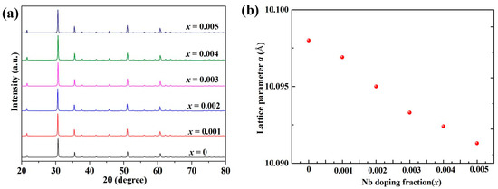
Figure 1.
(a) X-Ray Diffraction Profiles and (b) Lattice Constants of Nb-Doped Indium Oxide Thermoelectric Composites.

Table 1.
The refined results of Celref (when the Sigmas (the standard deviation) is refined to below 0.0005, the lattice parameters are supposed to be reliable).
From the electrical conductivity test curve of Nb-doped indium oxide thermoelectric materials in Figure 2a, it can be clearly observed that with the increase in Nb doping amount, the electrical conductivity of indium oxide thermoelectric materials shows an obvious upward trend. Without Nb doping, the electrical conductivity of pure indium oxide is relatively low, only about 53.42 S/cm; when the Nb doping amount reaches x = 0.005, the electrical conductivity of the material increases significantly to about 272.07 S/cm, with an increase of more than 5 times. The reasons for the improvement of electrical conductivity of indium oxide caused by Nb doping can be analyzed in depth from two aspects: the increase in carrier concentration and the change in carrier mobility. At the same time, combined with the donor effect of Nb element in the indium oxide lattice, the internal mechanism is revealed. The carrier concentration of indium oxide thermoelectric materials before and after Nb doping was characterized by Hall effect test as shown in Figure 2b. The results show that the carrier concentration of indium oxide increases significantly after Nb doping. The significant increase in carrier concentration is one of the main reasons for the increase in electrical conductivity of Nb-doped indium oxide, which is mainly attributed to the donor doping behavior of Nb element in the indium oxide lattice [18,19]. From the perspective of crystal structure, indium oxide has a cubic bixbyite structure, and In3+ ions occupy the cation positions in the lattice, forming a coordination structure with the surrounding O2− ions. The atomic number of Nb element is 41, and its common valence is +5, which is much higher than the +3 valence of In3+. When Nb element is doped into the indium oxide lattice, due to the similar ionic radius of Nb and In (the ionic radius of Nb is about 0.064 nm, and the ionic radius of In is about 0.080 nm), Nb can smoothly replace the In ions in the lattice, forming substitutional doping. During the substitution process, in order to maintain the electrical neutrality of the lattice, each Nb ion will release 2 free electrons into the lattice (because Nb carries 2 more positive charges than In, and 2 free electrons need to be released to balance the charge). These free electrons become carriers in the material, significantly increasing the number of carriers, thus greatly improving the carrier concentration. For Nb-doped In2O3, the NbIn** defects formed by Nb5+ substituting In3+ are typical donor defects. When Nb5+ is doped with In2O3, it will replace In3+ in the lattice. Due to the fact that Nb5+ has 2 more valence electrons than In3+, the excess electrons break free and become free electrons (donor state ionization), which act as carriers and directly increase the overall carrier concentration of the material.
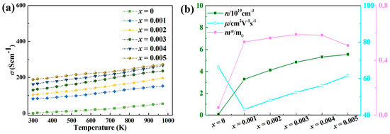
Figure 2.
(a) Electrical Conductivity Test Results and (b) Carrier Characteristic Detection Outcomes of Nb-Doped Indium Oxide Thermoelectric Composites (The green line represents the carrier concentration (n), the blue line represents the carrier mobility (μ), and the pink line represents the effective mass (m*)).
This equation indicates that Nb2O5, as the doping source, decomposes into 2 NbIn** defects (each carrying 2 positive charges after Nb5+ substitutes In3+), 2 free electrons (e′), and 5 lattice oxygen atoms (OOx, electrically neutral) in the In2O3 lattice. From the perspective of charge conservation, each Nb5+ ion has 2 more valence electrons than In3+; thus, each NbIn** defect can donate 2 free electrons to the conduction band. This process does not require breaking the covalent bonds of the host lattice, only overcoming the energy difference between the donor level and the conduction band edge. The donor effect is a common doping effect in semiconductor materials. When donor impurities (impurities that can provide free electrons to the semiconductor lattice) are doped into the semiconductor material, they ionize and release free electrons into the lattice, thereby increasing the carrier concentration in the material and improving its conductivity. In Nb doped indium oxide thermoelectric materials, Nb element serves as a typical donor impurity, and its donor effect is the core mechanism that leads to an increase in indium oxide carrier concentration and conductivity. From the perspective of electronic energy levels, indium oxide, as an n-type semiconductor material, has a certain bandgap width (approximately 3.5–3.7 eV) between the bottom of the conduction band and the top of the valence band [16,20,21]. In pure indium oxide, due to thermal excitation and other reasons, a small number of electrons will transition from the valence band to the conduction band, becoming free electrons, while leaving holes in the valence band. However, due to the large bandgap, the number of free electrons generated by thermal excitation is relatively small, resulting in a low carrier concentration and low conductivity of pure phase indium oxide. When Nb element is doped into the indium oxide lattice, Nb ions will form donor energy levels in the bandgap of indium oxide. The energy position of the donor energy level is close to the bottom of the conduction band, and the energy difference (donor ionization energy) between them is small. At lower temperatures, electrons at the donor level can absorb external energy (such as thermal energy) and ionize, transitioning into the conduction band and becoming free electrons. Each Nb ion can provide 2 free electrons, and a large number of Nb ions ionize and inject a large number of free electrons into the conduction band, significantly increasing the number of charge carriers in the conduction band. Different from the significant increase in carrier concentration, the carrier mobility of indium oxide thermoelectric materials shows a slight downward trend after Nb doping. The carrier mobility mainly depends on the scattering effect on the carriers when they move in the material lattice. The stronger the scattering effect, the lower the carrier mobility. The main reasons for the slight decrease in carrier mobility of indium oxide caused by Nb doping include the following aspects. First, there is a certain difference in ionic radius between Nb ions and In ions. Although substitutional doping can be formed between them, the difference in ionic radius will lead to local lattice distortion. This lattice distortion will form an additional potential field, which scatters the movement of carriers, thereby increasing the scattering probability of carriers and reducing the carrier mobility. Second, with the increase in Nb doping amount, the number of Nb ions in the lattice increases, and the Coulomb scattering between carriers and Nb ions also increases accordingly. Nb ions carry positive charges, while carriers (free electrons) carry negative charges, and there is a Coulomb attractive force between them. This Coulomb attractive force will interfere with the movement direction of carriers, causing the movement trajectory of carriers to deflect, increasing the number of scattering of carriers, and thus leading to the decrease in carrier mobility. Although Nb doping leads to a slight decrease in the carrier mobility of indium oxide, the increase range of carrier concentration is much larger than the decrease range of carrier mobility. According to the electrical conductivity formula σ = neμ, the contribution of carrier concentration increase to electrical conductivity dominates, so the overall electrical conductivity of indium oxide still shows a significant upward trend. Figure 3 and Figure 4 present comprehensive electronic property profiles of indium oxide before and after niobium (Nb) doping, including band structures, total density of states (DOS), and partial density of states (PDOS). These results clearly reveal the critical role of Nb doping in tailoring the electronic behavior of indium oxide, with the most prominent change being the narrowing of the band gap. In undoped indium oxide, the band gap exhibits a typical width corresponding to its intrinsic semiconductor characteristics, which imposes limitations on carrier excitation—only high-energy photons or external stimuli can overcome the band gap to promote electrons from the valence band (VB) to the conduction band (CB). However, after Nb doping, the band gap of the modified indium oxide is significantly reduced. This narrowing effect is highly beneficial for carrier excitation: it lowers the energy barrier required for electron transition between the VB and CB, enabling more electrons to be excited into the CB even under milder conditions (e.g., lower-energy light irradiation or moderate thermal activation). Concurrently, the increase in carrier concentration is a direct consequence of band gap narrowing. With a reduced energy barrier, a greater number of electrons are excited to the CB, while the VB leaves behind more holes. Both the elevated electron population in the CB and hole population in the VB contribute to a higher overall carrier concentration, which is crucial for enhancing the electrical conductivity of indium oxide. Another notable observation from the DOS profiles is the increased density of states near the Fermi level after Nb doping. The Fermi level, which represents the highest energy state occupied by electrons at absolute zero, serves as a critical reference for electronic behavior. The elevated DOS near Fermi level indicates a higher number of available electronic states around this energy level, facilitating more efficient electron transport. Collectively, the band gap narrowing and enhanced DOS near the Fermi level induced by Nb doping synergistically optimize the carrier excitation efficiency and carrier concentration, laying a solid foundation for its improved performance in optoelectronic and electronic devices.
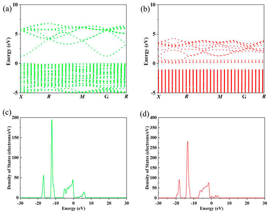
Figure 3.
Comparison of Electronic Band Diagrams (a,b) and Density of States (c,d) Between Undoped and Nb-Doped Indium Oxide ((a,c) for undoped; (b,d) for Nb doped).
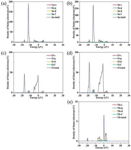
Figure 4.
Partial Density of States for Pure Indium Oxide (a,c) and Nb-Doped Indium Oxide (b,d,e).
The Seebeck coefficient (S) is one of the key parameters for evaluating the energy conversion efficiency of thermoelectric materials. Its value is closely related to the transport characteristics of carriers inside the material and directly affects the figure of merit (ZT) of thermoelectric materials. For indium oxide (In2O3)-based thermoelectric materials, the Seebeck coefficient is relatively low in the pure phase, which limits the improvement of their thermoelectric conversion performance. Previous studies have confirmed that Nb doping can significantly improve the electrical conductivity of indium oxide, and there is a complex coupling relationship between the Seebeck coefficient, electrical conductivity, carrier concentration, and mobility. Based on the Seebeck coefficient test results of Nb-doped indium oxide thermoelectric materials in Figure 5a, combined with the existing data of electrical conductivity, carrier concentration, and mobility, this paper systematically analyzes the internal mechanism of the increase in Seebeck coefficient caused by Nb doping from the perspective of donor effect regulating carrier transport, providing theoretical support for optimizing the comprehensive performance of In2O3-based thermoelectric materials. It can be clearly observed from the Seebeck coefficient test curve in Figure 5a that the regulation of Nb doping on the absolute value of the Seebeck coefficient of indium oxide shows a significant downward trend. The absolute value of the Seebeck coefficient of pure indium oxide at room temperature (300 K) is relatively high, about −185.24 μV/K, the negative sign indicates its n-type semiconductor characteristics; with the increase in Nb doping amount, the absolute value of the Seebeck coefficient gradually decreases. When the Nb doping amount reaches x = 0.005, the absolute value of the room-temperature Seebeck coefficient drops to −120.12 μV/K, with a decrease of more than 30%. This downward trend persists throughout the entire test temperature range, and with the increase in temperature, the difference in the absolute value of the Seebeck coefficient between the Nb-doped sample and the pure phase sample further expands. It is worth noting that the decrease in the absolute value of the Seebeck coefficient occurs simultaneously with the increase in electrical conductivity. This phenomenon of “increasing electrical conductivity-decreasing absolute value of Seebeck coefficient” is essentially a direct manifestation of the reduction in energy difference during carrier transport after the rapid increase in carrier concentration, and the donor effect plays a core regulatory role in this process. With the increase in Nb doping, the ionization degree of donor impurities continues to improve, and the carrier concentration increases exponentially. The Seebeck coefficient is negatively correlated with the carrier concentration. When the carrier concentration approaches the effective density of states in the conduction band, this change has a much greater inhibitory effect on the absolute value of the Seebeck coefficient than the positive contribution brought by the Fermi level shift. At the same time, a large number of free electrons are filled into the conduction band, causing the energy distribution of electrons to become more concentrated (most electrons are in the low-energy region of the conduction band), significantly reducing the energy difference between charge carriers and further leading to a decrease in the absolute value of the Seebeck coefficient.
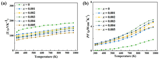
Figure 5.
(a) Seebeck Coefficient Test Data and (b) Power Factor Characterization Results of Nb-Doped Indium Oxide-Based Thermoelectric Materials.
After Nb doping, although the increase in carrier concentration leads to a slight decrease in the absolute value of the Seebeck coefficient, the decrease range of the square of the Seebeck coefficient is far smaller than the increase range of electrical conductivity. Under the synergistic effect of the two, the power factor still shows a significant upward trend as shown in Figure 5b. In addition, the negative impact of the slight decrease in mobility on the power factor is negligible: the decrease in mobility only slightly narrows the growth range of electrical conductivity, but does not change the overall trend of the multiple-order growth of electrical conductivity, and does not cause obvious negative interference to the Seebeck coefficient. At the same time, in the medium-and high-temperature range, the electrical conductivity of the Nb-doped sample changes gently with temperature, and the decrease range of the absolute value of the Seebeck coefficient is smaller than that of the pure phase sample, so that the power factor still maintains a high level at high temperatures with the highest value of ~5.10 μW/(cm·K2), while that of the pure phase sample is only ~1.83 μW/(cm·K2). This high-temperature stability further highlights the optimization effect of Nb doping on the power factor, providing a guarantee for the application of In2O3.
In the pure phase state, indium oxide (In2O3)-based thermoelectric materials have a regular lattice structure, weak phonon scattering, and high lattice thermal conductivity, resulting in high overall thermal conductivity, which limits the improvement of the ZT value. Previous studies have confirmed that Nb doping can improve the power factor, electrical conductivity, and carrier concentration of indium oxide through the donor effect, accompanied by a slight decrease in mobility. Based on the thermal conductivity and lattice thermal conductivity test data of Nb-doped indium oxide in Figure 6a,b, combined with the above-mentioned variation laws of electrical properties, this paper systematically reveals the internal mechanism of the decrease in thermal conductivity and lattice thermal conductivity from the perspective of phonon scattering regulation and the synergistic effect of electronic thermal conductivity, providing theoretical support for further optimizing the ZT value of In2O3-based thermoelectric materials. It can be clearly observed from the thermal conductivity test curve in Figure 6 that Nb doping has a significant reducing effect on both the overall thermal conductivity (κ) and lattice thermal conductivity (κ1) of indium oxide. The thermal conductivity of indium oxide is jointly determined by electronic thermal conductivity and lattice thermal conductivity. The regulation of thermal conductivity by Nb doping is the result of the synergistic effect of the significant decrease in lattice thermal conductivity and the slight change in electronic thermal conductivity. When Nb is substitutionally doped in the indium oxide lattice, there is a significant difference in ionic radius between Nb and In3+ (the ionic radius of Nb is about 0.064 nm, and the ionic radius of In3+ is about 0.080 nm). This mismatch in ionic radius could lead to local lattice distortion [22,23]. In pure indium oxide, the lattice atoms are arranged regularly, the scattering effect on phonons during transport is weak, the average phonon mean free path is long, and the lattice thermal conductivity is high; after Nb replaces In3+, lattice distortion could form additional potential field disturbance, which strongly scatters the transport of phonons. Nb doping significantly increases the carrier concentration of indium oxide. The electronic thermal conductivity in Figure 6c increases with the increase in doping amount, which should be caused by the increase in conductivity.
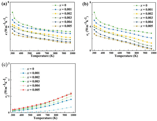
Figure 6.
(a) Thermal Conductivity Test Spectra and (b) Lattice Thermal Conductivity Characterization Results of Nb-Doped Indium Oxide-Based Thermoelectric Materials and (c) Electrical Thermal Conductivity.
Based on the ZT value test data of Nb-doped indium oxide in Figure 7, combined with the above-mentioned variation laws of electrical and thermal properties, this paper systematically reveals the internal mechanism of ZT value increase, providing key theoretical and experimental basis for the performance optimization of In2O3-based thermoelectric materials. t can be clearly observed from the ZT value test curve in Figure 7 that Nb doping has a significant and temperature-dependent effect on improving the ZT value of indium oxide. At room temperature (300 K), the ZT value of pure indium oxide is extremely low, only 3.99138 × 10⁻⁵; with the increase in Nb doping amount, the ZT value shows a continuous upward trend. When the Nb doping amount reaches x = 0.005, the room-temperature ZT value increases to 0.009. In the medium-and high-temperature range, the improvement effect of ZT value is more significant: the ZT value of pure indium oxide increases slowly with temperature, only 0.055 at 973 K; while the ZT value of the Nb-doped sample with x = 0.004 increases rapidly with temperature, reaching 0.302 at 973 K, which is over 5 times higher than that of the pure phase sample, but also much higher than the ZT value at room temperature, and higher than 0.18 for Ge doping [14], 0.09 for Mo doping [10], but lower than 0.42 for V doping [11].
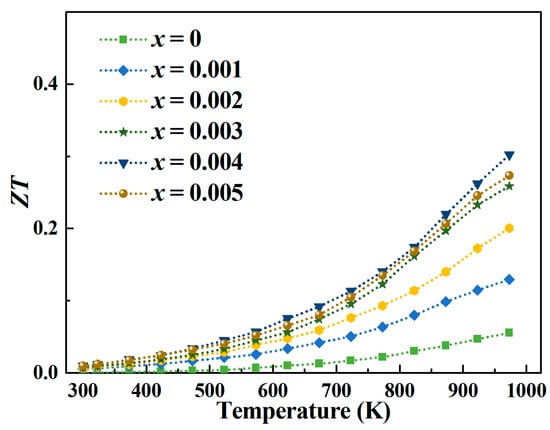
Figure 7.
ZT Characteristic Test Results of Niobium-Doped Indium Oxide Thermoelectric Material.
The Vickers hardness (HV) is a key indicator for evaluating the mechanical properties of materials, reflecting the material’s ability to resist local plastic deformation. Its value is closely related to the material’s lattice structure, chemical bond strength, defect concentration, and atomic arrangement density. For indium oxide (In2O3)-based thermoelectric materials, excellent thermoelectric performance (such as high ZT value) needs to be matched with good mechanical properties to meet the requirements for material mechanical stability in practical applications. Pure indium oxide has a low Vickers hardness score due to its relatively loose lattice structure and weak interatomic bonding, which limits its application in wear-resistant and impact-resistant scenarios. Based on the Vickers hardness test data of Nb-doped indium oxide in Figure 8, combined with the variation laws of thermoelectric performance parameters such as thermal conductivity, power factor, and electrical conductivity, this paper systematically reveals the internal mechanism of the increase in Vickers hardness caused by Nb doping, providing theoretical and experimental support for the “synergistic optimization of thermoelectric-mechanical properties” of In2O3-based thermoelectric materials. t can be clearly observed from the Vickers hardness test curve in Figure 8 that Nb doping has a significant and dose-dependent effect on improving the Vickers hardness of indium oxide. The essence of the Vickers hardness is the material’s lattice resistance to external pressure, and its value depends on the interatomic bonding strength, lattice density, and the inhibitory effect of defects on plastic deformation. When Nb is substitutionally doped in the indium oxide lattice, the difference in ionic radius between Nb and In3+ (Nb is about 0.064 nm, In is about 0.080 nm) will cause significant lattice distortion-after the smaller Nb replaces the larger In3+, the coordination environment of the surrounding O2− ions changes, and O2− will slightly shift towards Nb, forming a locally “compact” lattice region. This lattice distortion will lead to the shortening of the interatomic bond length, and the shortening of the bond length directly enhances the bonding strength of the ionic bond (according to Coulomb’s law, the shorter the bond length, the stronger the electrostatic force between ions). In pure indium oxide, the longer In-O bond leads to weak interatomic bonding force, and lattice slip is easy to occur under external pressure, showing low hardness; after Nb doping, the introduction of Nb-O short bonds and the “stress field” generated by lattice distortion will hinder the occurrence of lattice slip-the slip plane needs to overcome stronger interatomic forces to move, thereby significantly improving the material’s resistance to plastic deformation, manifested as an increase in Vickers hardness. In addition, there is a direct correlation between lattice distortion and the decrease in thermal conductivity: the distorted lattice strongly scatters phonons, and this structural feature also provides a structural basis for hardness improvement, realizing the synergistic regulation of “thermal-mechanical properties”. Nb doping releases free electrons. The introduction of a large number of free electrons will change the distribution state of the electron cloud in the lattice—the density of the electron cloud around the ion nucleus increases, forming a more “dense” electron cloud barrier. On the one hand, electron cloud densification enhances the metallic bond component between atoms (although indium oxide is mainly composed of ionic bonds, the increase in carrier concentration will increase the contribution of metallic bonds), and the high-ductility and high-strength characteristics of metallic bonds can further improve the material’s deformation resistance; on the other hand, the dense electron cloud will inhibit the movement of dislocations-when dislocations migrate in the lattice, they need to break through the “energy barrier” formed by the electron cloud, and the increase in dislocation migration resistance directly reduces the plastic deformation ability of the material, thereby improving the Vickers hardness. It is worth noting that the increase in carrier concentration occurs synchronously with the optimization of electrical conductivity and power factor: the increase in free electrons not only enhances conductivity but also helps reduce lattice thermal conductivity through electron-phonon scattering, and the mechanical strengthening effect brought by electron cloud densification further improves the synergistic optimization mechanism of “thermoelectric-mechanical properties”.
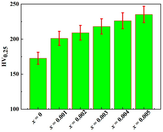
Figure 8.
Vickers Hardness Characterization Results of Nb-Doped Indium Oxide-Based Thermoelectric Material.
3. Experimental Part
High-purity indium oxide (In2O3, 99.99%, Sinopharm Group, Beijing, China) and niobium pentoxide (Nb2O5, 99.99%, Sinopharm Group) powders were selected as raw materials. A planetary ball mill was utilized for mechanical alloying to fabricate Nb-doped In2O3 powder (In2-xNbxO3, x = 0.001, 0.002, 0.003, 0.004, 0.005). Stoichiometric quantities of In2O3 and Nb2O5 powders corresponding to preset molar ratios of Nb doping were thoroughly blended. The stainless steel ball mill jar is used, and it is thoroughly dried with sawdust and alcohol beforehand. Put the weighed powder into a ball milling tank for 10 h with the speed of 450 rpm and the ball/material ratio of 20:1, then add anhydrous ethanol, ball milling with a planetary ball mill (QM-2SP12, Nanjing University Instrument Factory, Nanjing, China) for 1 h with the speed of 300 rpm, and then dry the obtained powder for more than 48 h at the temperature of 373 K. Then place the obtained powder into a quartz tube, fill it with argon gas for protection, and seal it. Put it into a muffle furnace and calcine at high temperature of 1473 K for 8 h. Crush the obtained sample and then perform discharge plasma sintering at the temperature of 1273 K with 30 min of insulation and a pressure of 60 MPa [24]. Diffractometer is used to characterize the phase structure of the material, and the equipment is Bruker AXS D8 diffractometer (Bruker AXS GmbH, Karlsruhe, Germany). The diffraction analysis adopts Cu & rays with a wavelength of 1.5406 Å. Nickel plates was used as the substrate on the XRD sample stage with a diffraction angle range of 10–80°, a step size of 0.02°, a tube current of 20 mA, and a tube voltage of 40 kV. The electrical conductivity and Seebeck coefficient were tested using an electrical performance tester (ZEM-3, ULVAC KIKO, Tokyo, Japan). The carrier concentration and mobility at room temperature were measured by the van der Pauw method using the Hall-effect measurement system (HMS-5500, Ekopia, Seoul, Republic of Korea). The volume density was measured by the Archimedes method. The relative densities were 97.13%, 97.25%, 97.36%, 97.29%, 97.27%, and 97.32% for x = 0, 0.001, 0.002, 0.003, 0.004, and 0.005, respectively. The flash thermal conductivity tester used was LFA457 (Netzsch, Berlin, Germany), Germany, for thermal conductivity testing. And the specific heat capacity (Cp) was determined by differential scanning calorimetry (DSC 404C, Netzsch, Berlin, Germany) under Inert atmosphere. All the specimens were polished with two parallel planes and the plane close to the central part was utilized for Vickers hardness (HV) measurement, which were conducted on HV-10008 with a load of 25 g and a loading time of 15 s. Every sample was tested with 5 data points, and the average HV was used for characterizing mechanical properties. The uncertainty of the Vickers hardness is estimated to be within 5%. The uncertainty of the Seebeck coefficient and electrical conductivity measurements was 5%. The uncertainty of the thermal conductivity is estimated to be within 8%, considering the uncertainties regarding thermal diffusion coefficient, specific heat, and density. The combined uncertainty for all measurements involved in the calculation of ZT is less than 15%. The density functional calculation used here is the CASTEP software package in the materials studio software 8.0, and the constructed 2 × 2 × 1 unit cell is calculated. The cut-off energy in plane wave expansion is 550 eV, the total energy is converged to less than 2.0 × 10⁻⁵ eV/atom. The maximum stress, maximum force were converged to less than 0.05 GPa and 0.3 eV/nm. The tolerance in the self-consistent field (SCF) calculation was set to 10−6 eV/atom.
4. Conclusions
This study systematically investigated the regulatory mechanism of Nb doping on the structure, thermoelectric properties, and mechanical properties of indium oxide (In2O3) thermoelectric materials, with the main conclusions as follows: Firstly, phase analysis showed that the XRD peaks of Nb-doped In2O3 samples prepared by mechanical alloying and spark plasma sintering (SPS) were consistent with the In2O3 standard card. With the increase in Nb doping concentration, the lattice constant decreased gradually due to the ionic radius difference between Nb (64 pm) and In3+ (80 pm). Secondly, in terms of thermoelectric properties, Nb significantly improved the electrical conductivity of the material. When the Nb doping concentration x = 0.005, electrical conductivity reached 272.07 S/cm, which was more than 5 times higher than that of pure In2O3 (53.42 S/cm). This was due to the free electrons released when Nb replaced In3+, resulting in a substantial increase in carrier concentration, and the increase in the amplitude of carrier concentration was much larger than the slight decrease in the amplitude of carrier mobility. Although Nb doping reduced the absolute value of the Seebeck coefficient (from −185.24 μV/K to −120.12 μV/K when x = 0.005), the significant increase in electrical conductivity dominated the power factor, which reached a maximum of 5.10 μW/(cm·K2), which is much higher than that of the pure phase (1.83 μW/(cm·K2)). The sample with x = 0.004 had a ZT value of 0.302 at 973 K, which was more than 5 times higher than that of the pure phase (0.055 at 973 K). Thirdly, in terms of mechanical properties, Nb doping increased the Vickers hardness of the material, which was attributed to lattice distortion shortening the bond length and enhancing ionic bond strength, thus realizing the synergistic optimization of thermoelectric and mechanical properties.
Author Contributions
Conceptualization, W.L. and T.T.; methodology, T.X.; software, R.R.; validation, P.J., G.Z. and H.Z. (Haitao Zhang); formal analysis, B.F.; investigation, H.Z. (Heng Zhao); resources, B.F.; data curation, H.Z. (Haitao Zhang); writing—original draft preparation, H.Z. (Haitao Zhang); writing—review and editing, T.X.; visualization, T.T.; supervision, T.X.; project administration, H.Z. (Heng Zhao); funding acquisition, T.X. All authors have read and agreed to the published version of the manuscript.
Funding
This research is supported by the Sichuan Key Laboratory of Smart Grids (2023-IEPGKLSP-KFYB04); the Hubei Provincial Key Laboratory for Operation and Control of Cascaded Hydropower Stations (China Three Gorges University, 2023KJX02); the Doctoral Initiation Fund Project of Hubei University of Science and Technology (BK202335); the Research on Monitoring System Based on Gear Transmission Vibration Signals (2025HX026); the Research and development of environmentally friendly coating surface gloss powder (2024HX161); the Research Fund for the Key Laboratory of Geological Hazards in the Three Gorges Reservoir Area (China Three Gorges University); the Ministry of Education Fund Project [2023KDZ08]; the Guiding Project of the Scientific Research Plan of the Hubei Provincial Department of Education in 2024 (B2024159); and the Science and Technology Talents Serving Enterprises Project of the Hubei Provincial Department of Science and Technology (2025DJB057).
Data Availability Statement
The original contributions presented in this study are included in the article. Further inquiries can be directed to the corresponding author.
Conflicts of Interest
The authors declare no conflict of interest.
References
- Jan, R.; Fayaz, M.; Ayoub, N.; Islam, I.; Ghosh, S.; Rubab, S.; Khandy, S.A. Oxide thermoelectric materials: A review of emerging strategies for efficient waste heat recovery. J. Power Sources 2025, 654, 237806. [Google Scholar] [CrossRef]
- Liu, Y.; Zhi, J.; Li, W.; Yang, Q.; Zhang, L.; Zhang, Y. Oxide materials for thermoelectric conversion. Molecules 2023, 28, 5894. [Google Scholar] [CrossRef] [PubMed]
- Zhao, Z.; Zhang, X.; Zhao, L.D. Strategies for manipulating thermoelectric properties of layered oxides. Matter 2023, 6, 3274–3295. [Google Scholar] [CrossRef]
- Tang, W.; Qian, W.; Jia, S.; Li, K.; Zhou, Z.; Lan, J.; Yang, X. BiCuSeO based thermoelectric materials: Innovations and challenges. Mater. Today Phys. 2023, 35, 101104. [Google Scholar] [CrossRef]
- Sulaiman, S.; Sudin, I.; Al-Naib, U.M.B.; Omar, M.F. Review of the nanostructuring and doping strategies for high-performance ZnO thermoelectric materials. Crystals 2022, 12, 1076. [Google Scholar] [CrossRef]
- Song, X.; Wang, G.; Zhou, L.; Yang, H.; Li, X.; Yang, H.; Wang, N. Oxide perovskite BaSnO3: A promising high-temperature thermoelectric material for transparent conducting oxides. ACS Appl. Energy Mater. 2023, 6, 9756–9763. [Google Scholar] [CrossRef]
- Ge, B.; Li, R.; Wang, G.; Zhu, M.; Zhou, C. Oxide semiconductors for thermoelectric: The challenges and future. J. Am. Ceram. Soc. 2024, 107, 1985–1995. [Google Scholar] [CrossRef]
- Zhang, P.; Lou, Z.; Gong, L.; Wu, Z.; Chen, X.; Xu, W.; Wang, Y.; Xu, J.; Dachevsky, Z.; Gao, F. Development and applications of thermoelectric oxide ceramics and devices. Energies 2023, 16, 4475. [Google Scholar] [CrossRef]
- Caballero-Calero, O.; Ares, J.R.; Martín-González, M. Environmentally friendly thermoelectric materials: High performance from inorganic components with low toxicity and abundance in the earth. Adv. Sustain. Syst. 2021, 5, 2100095. [Google Scholar] [CrossRef]
- Klich, W.; Ohtaki, M. Thermoelectric properties of Mo-doped bulk In2O3 and prediction of its maximum ZT. Ceram. Int. 2021, 47, 18116–18121. [Google Scholar] [CrossRef]
- Ahmad, A.; Hussain, M.; Zhou, Z.; Liu, R.; Lin, Y.H.; Nan, C.W. Thermoelectric performance enhancement of vanadium doped n-type In2O3 ceramics via carrier engineering and phonon suppression. ACS Appl. Energy Mater. 2019, 3, 1552–1558. [Google Scholar] [CrossRef]
- Tie, J.; Hu, Y.; Ma, Z.; Zhang, F. Optimizing Carrier Concentration and Phonon ScatteringSynergistically to Enhance Thermoelectric Performance in Cu2Se-Based Materials. J. Alloys Compd. 2025, 10, 183787. [Google Scholar] [CrossRef]
- Song, C.; Zhou, H.; Gu, Y.; Pan, L.; Chen, C.; Wang, Y. Enhanced thermoelectric properties of Bi2O2Se by Bi2Te2.7Se0.3 addition. J. Alloys Compd. 2023, 930, 167439. [Google Scholar] [CrossRef]
- Combe, E.; Guilmeau, E.; Savary, E.; Marinel, S.; Cloots, R.; Funahashi, R.; Boschini, F. Microwave sintering of Ge-doped In2O3 thermoelectric ceramics prepared by slip casting process. J. Eur. Ceram. Soc. 2015, 35, 145–151. [Google Scholar] [CrossRef]
- Wu, H.; Chen, L.; Ning, S.; Zhao, X.; Deng, S.; Qi, N.; Ren, F.; Chen, Z.; Tang, J. Extremely low thermal conductivity and enhanced thermoelectric performance of porous Gallium-doped In2O3. ACS Appl. Energy Mater. 2021, 4, 12943–12953. [Google Scholar] [CrossRef]
- Liu, Y.; Lin, T.; Huang, R.; Shi, J.; Chen, S. Analysis of the Effect of Copper Doping on the Optoelectronic Properties of Indium Oxide Thin Films and the Thermoelectric Properties of an In2O3/Pt Thermocouple. Crystals 2024, 14, 78. [Google Scholar] [CrossRef]
- Hsin, C.L.; Hsiao, J.C.; Chen, Y.M.; Lee, S.W. Thermoelectric properties of Zn-and Ce-alloyed In2O3 and the effect of SiO2 nanoparticle additives. Nanotechnology 2022, 33, 135712. [Google Scholar] [CrossRef] [PubMed]
- Feng, B.; Xu, Y.; Yang, S.; Ruan, R.; Zhang, R.; Xiong, T.; Xu, B.; Zheng, Z.; Zhao, G.; Zhang, Y.; et al. Correlation-based influence mechanism of aluminum doping on the thermoelectric properties of In2O3-based materials. J. Mater. Sci. Mater. Electron. 2025, 36, 253. [Google Scholar] [CrossRef]
- Korotcenkov, G.; Brinzari, V.; Ham, M.H. In2O3-based thermoelectric materials: The state of the art and the role of surface state in the improvement of the efficiency of thermoelectric conversion. Crystals 2018, 8, 14. [Google Scholar] [CrossRef]
- Nielsen, I.G.; Sommer, S.; Iversen, B.B. Phase control for indium oxide nanoparticles. Nanoscale 2021, 13, 4038–4050. [Google Scholar] [CrossRef]
- Gautam, R.; Singh, A.; Verma, A.; Nautiyal, V.K.; Yadav, B.C.; Chaudhary, V. A novel nanoparticles spilled-over In2O3 microcubes-enabled sustainable chemiresistor for environmental carbon dioxide monitoring. Nanotechnology 2024, 35, 435502. [Google Scholar] [CrossRef]
- Lo, S.H.; He, J.; Biswas, K.; Kanatzidis, M.G.; Dravid, V.P. Phonon scattering and thermal conductivity in p–type nanostructured PbTe–BaTe bulk thermoelectric materials. Adv. Funct. Mater. 2012, 22, 5175–5184. [Google Scholar] [CrossRef]
- Ortiz, B.R.; Peng, H.; Lopez, A.; Parilla, P.A.; Lany, S.; Toberer, E.S. Effect of extended strain fields on point defect phonon scattering in thermoelectric materials. Phys. Chem. Chem. Phys. 2015, 17, 19410–19423. [Google Scholar] [CrossRef] [PubMed]
- Zhao, H.; Feng, B.; Yang, S.; Ruan, R.; Zhang, R.; Xiong, T.; Xu, B.; Zheng, Z.; Zhao, G.; Zhang, Y.; et al. Analysis of the Influence Mechanism of Ti Doping on the Properties of In2O3 Thermoelectric Materials. Ceram. Int. 2025, 15, 42897. [Google Scholar] [CrossRef]


Disclaimer/Publisher’s Note: The statements, opinions and data contained in all publications are solely those of the individual author(s) and contributor(s) and not of MDPI and/or the editor(s). MDPI and/or the editor(s) disclaim responsibility for any injury to people or property resulting from any ideas, methods, instructions or products referred to in the content. |
© 2025 by the authors. Licensee MDPI, Basel, Switzerland. This article is an open access article distributed under the terms and conditions of the Creative Commons Attribution (CC BY) license (https://creativecommons.org/licenses/by/4.0/).