A Novel Design of Optical Switch Based on Guided Mode Resonances in Dielectric Photonic Crystal Structures

 ,
,  ,
, 
 ,
,  and
and 
Abstract
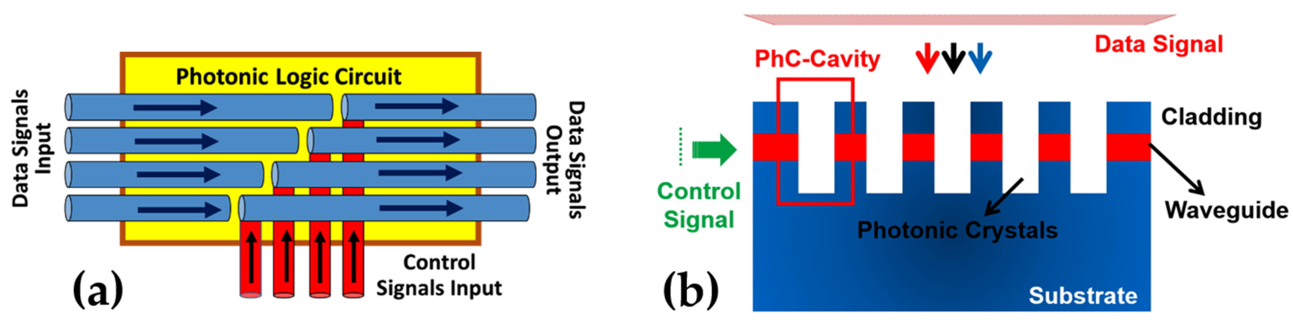
:1. Introduction
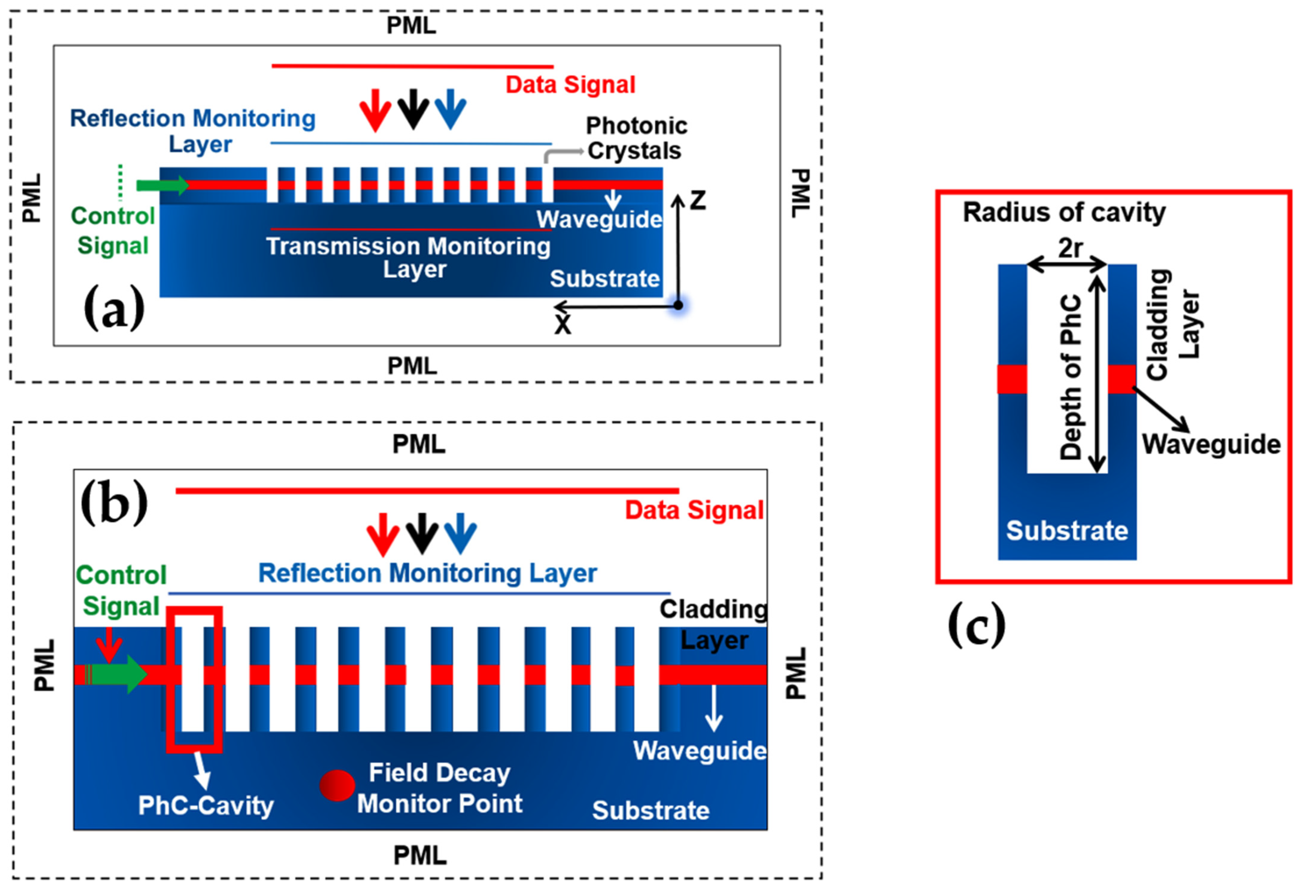
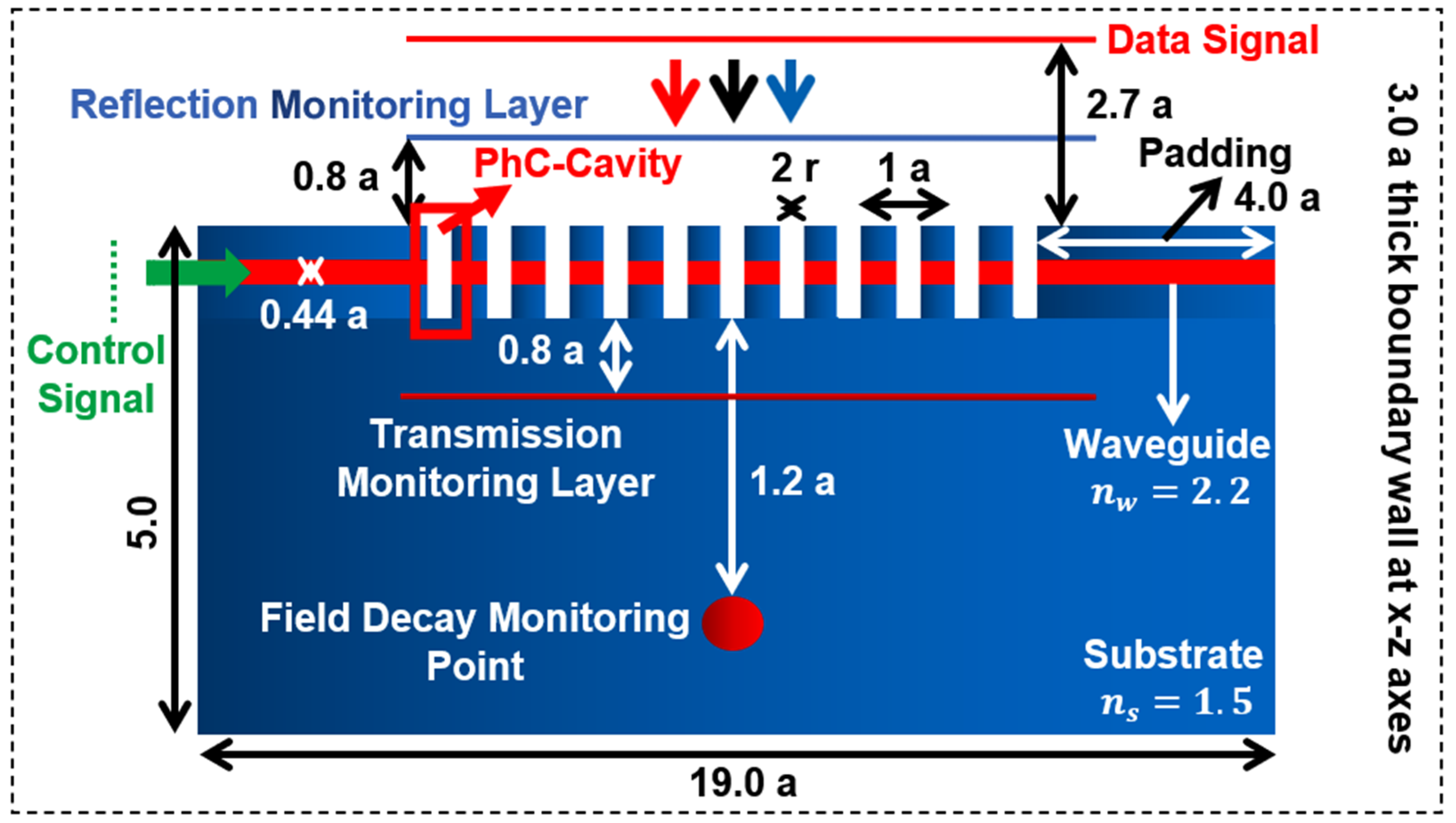
2. Simulation Approach
3. Designing Parameters
4. Results
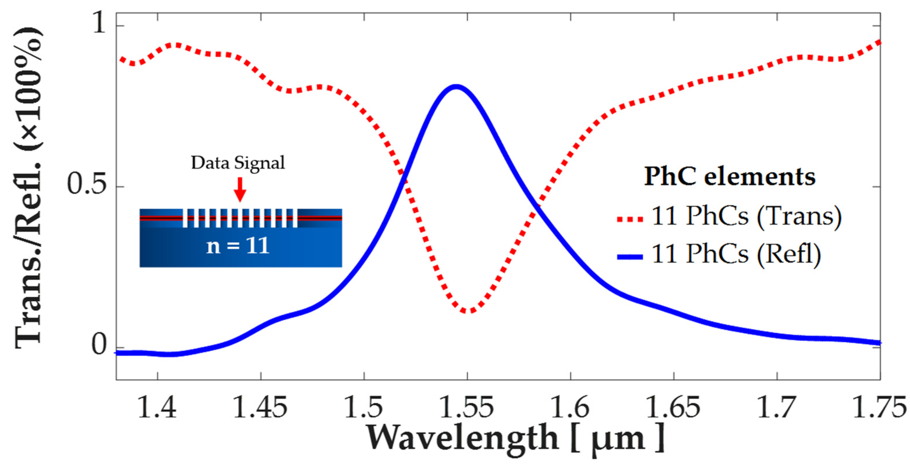
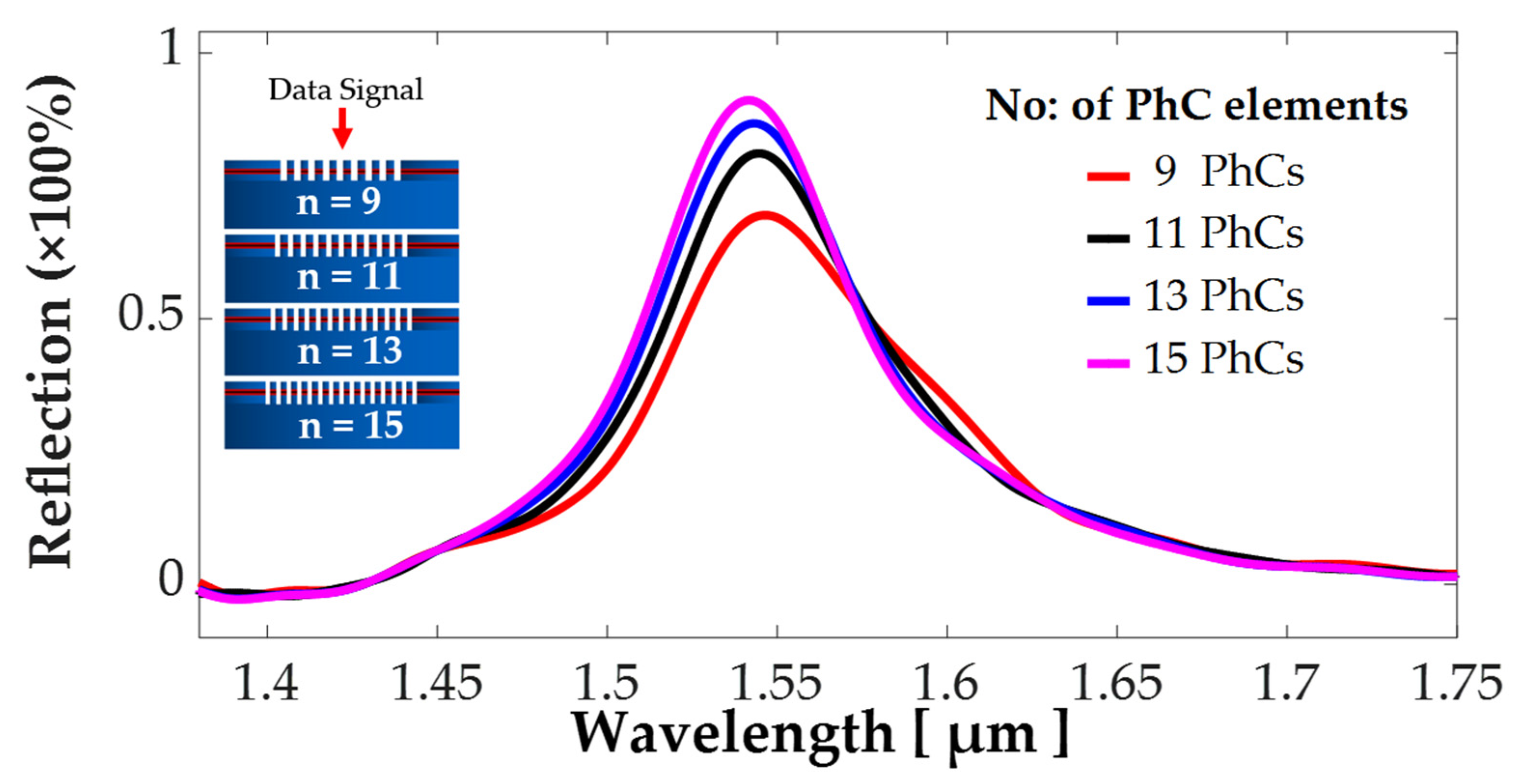
4.1. Effect of the Number of PhC Elements on A Data Signal
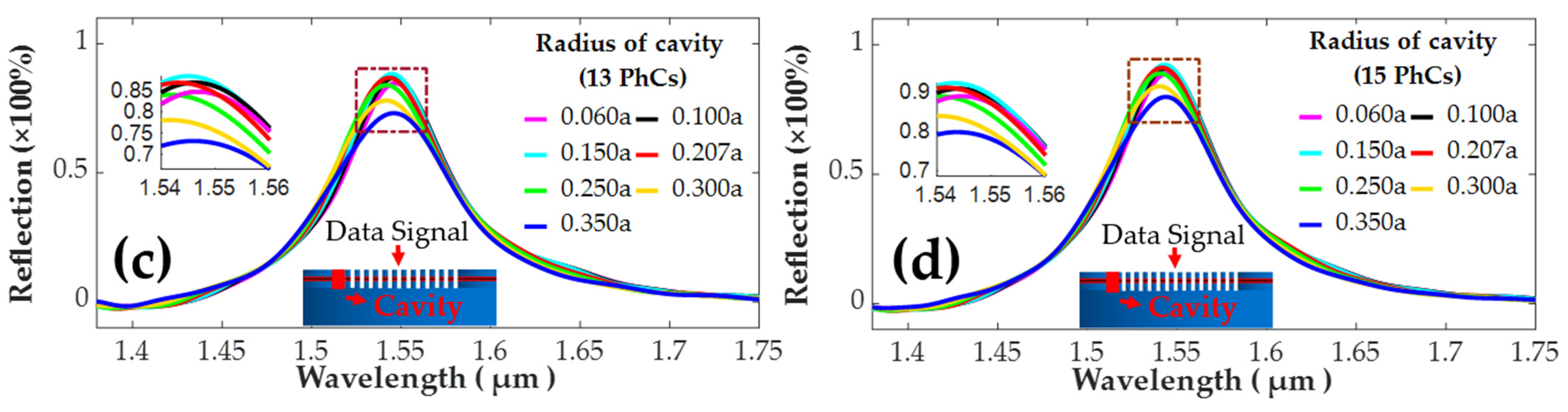
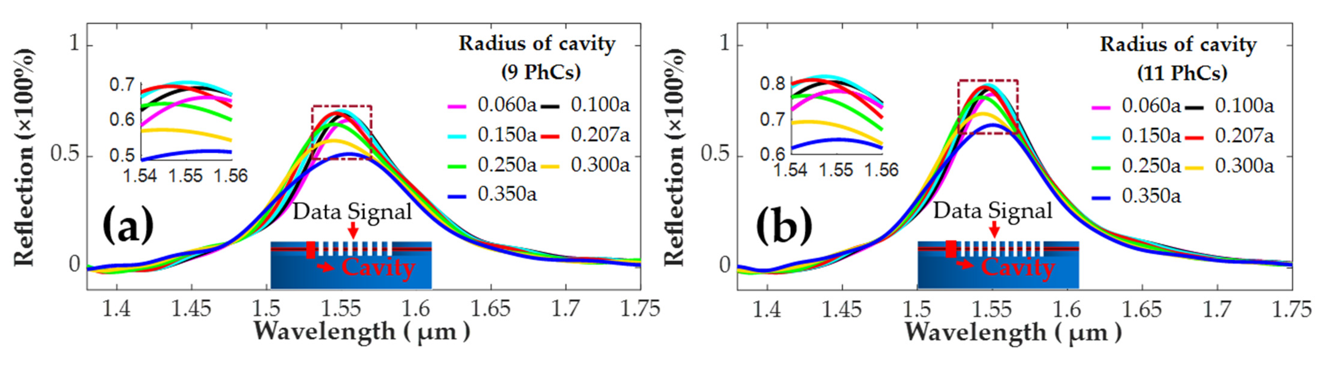
4.2. Effect of the Radius of PhC-Cavity with A Data Signal
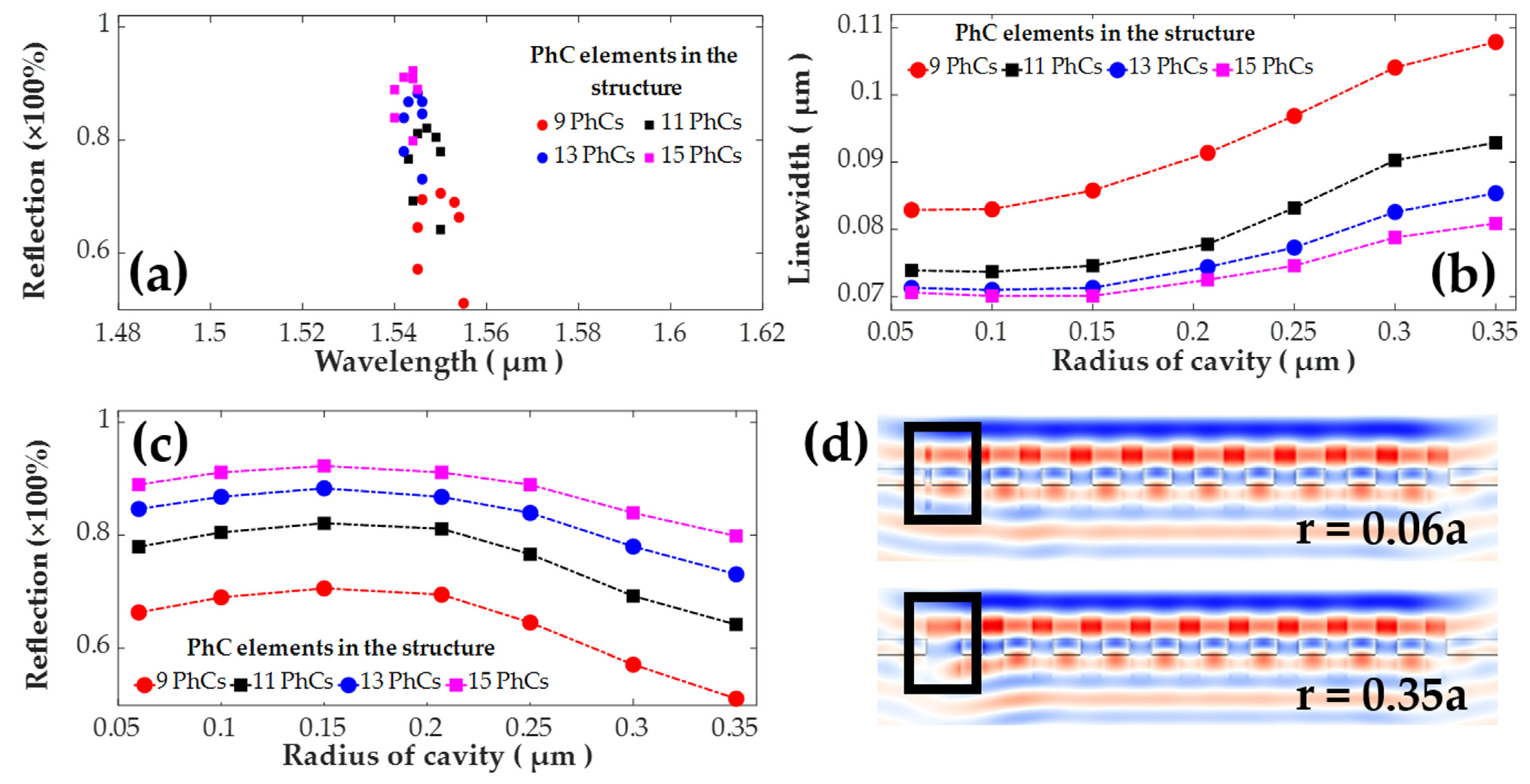
4.3. Comparative Analysis of Spectral Properties for Variation in the Number of PhC-Elements and Radius of PhC-Cavity for Data Source
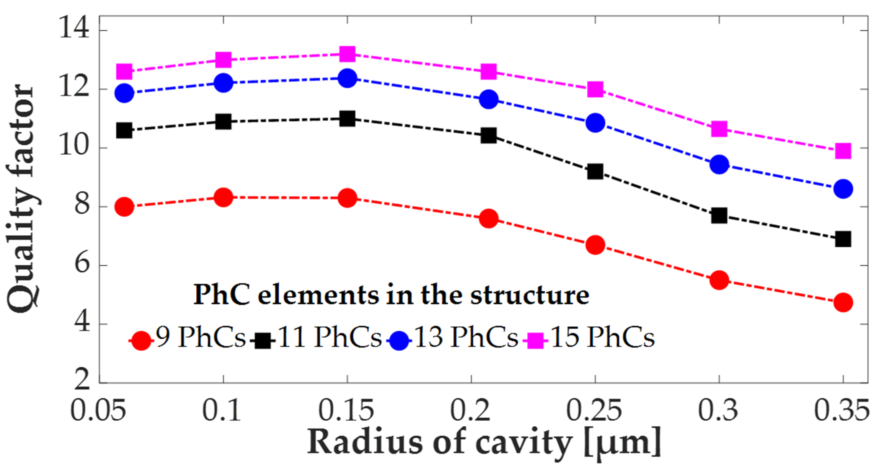
4.4. Analysis of the Quality Factor for the Variation in the Number of PhC-Elements and Radius of PhC-Cavity for Data Source
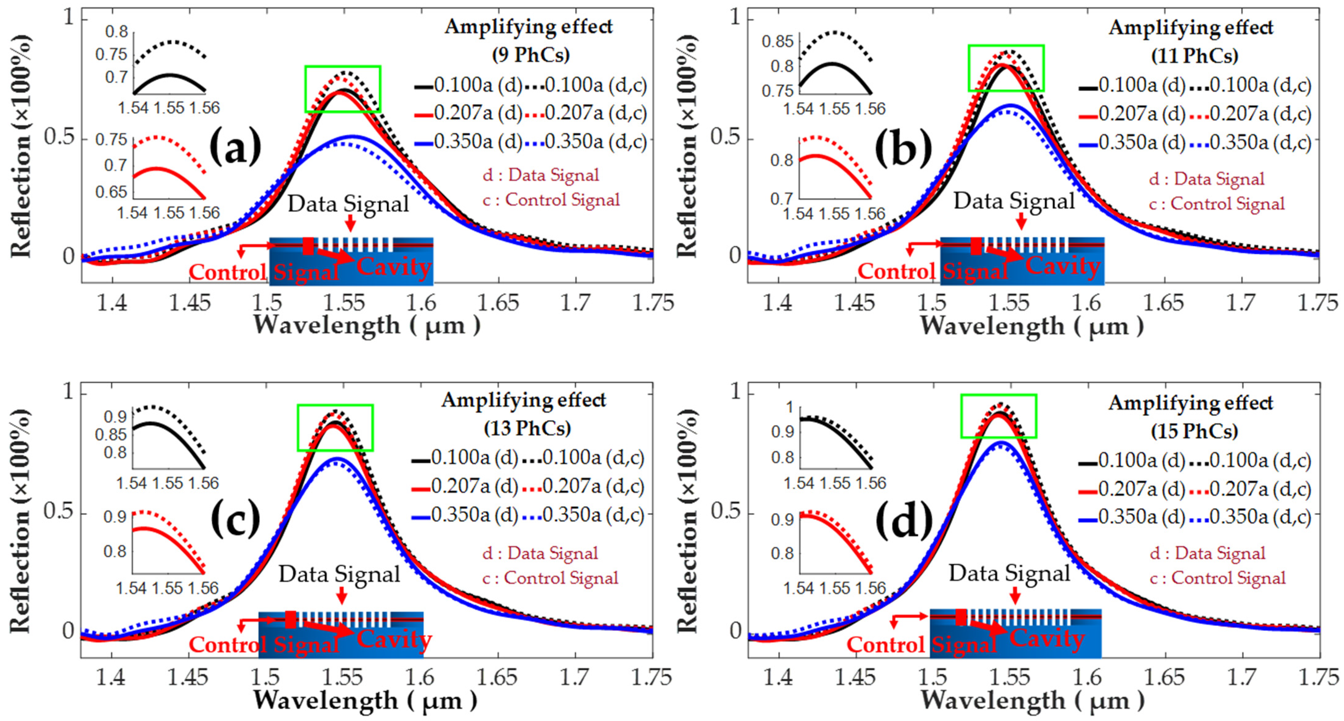
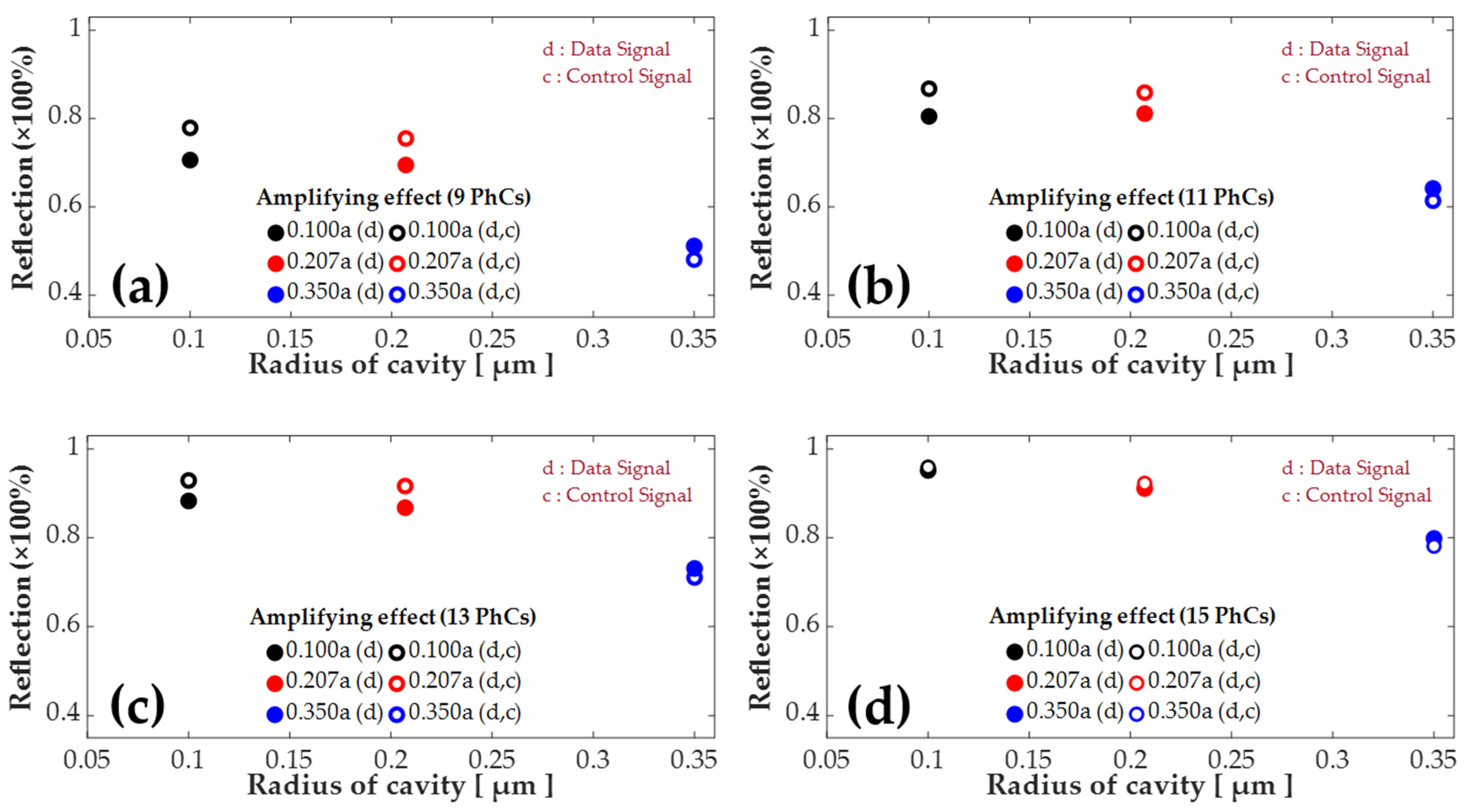
4.5. Transistor Action in Different PhCs Structures Using Both the Signals (Data and Control)
4.6. Comparative Analysis of Reflection Peak against Variation in the Number of PhC Elements for Optical Switching Action
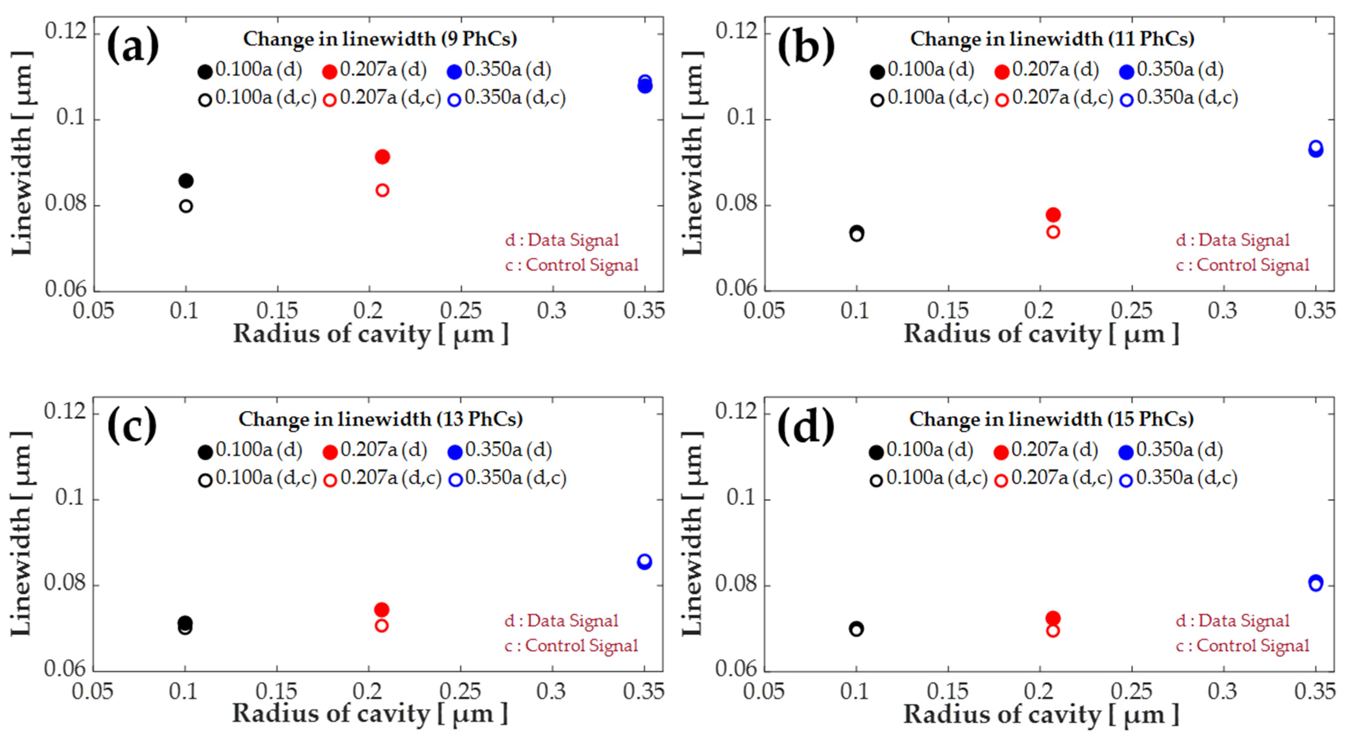
4.7. Comparative Analysis of the Linewidth against Variation in the Number of PhC Elements for Optical Switching Action
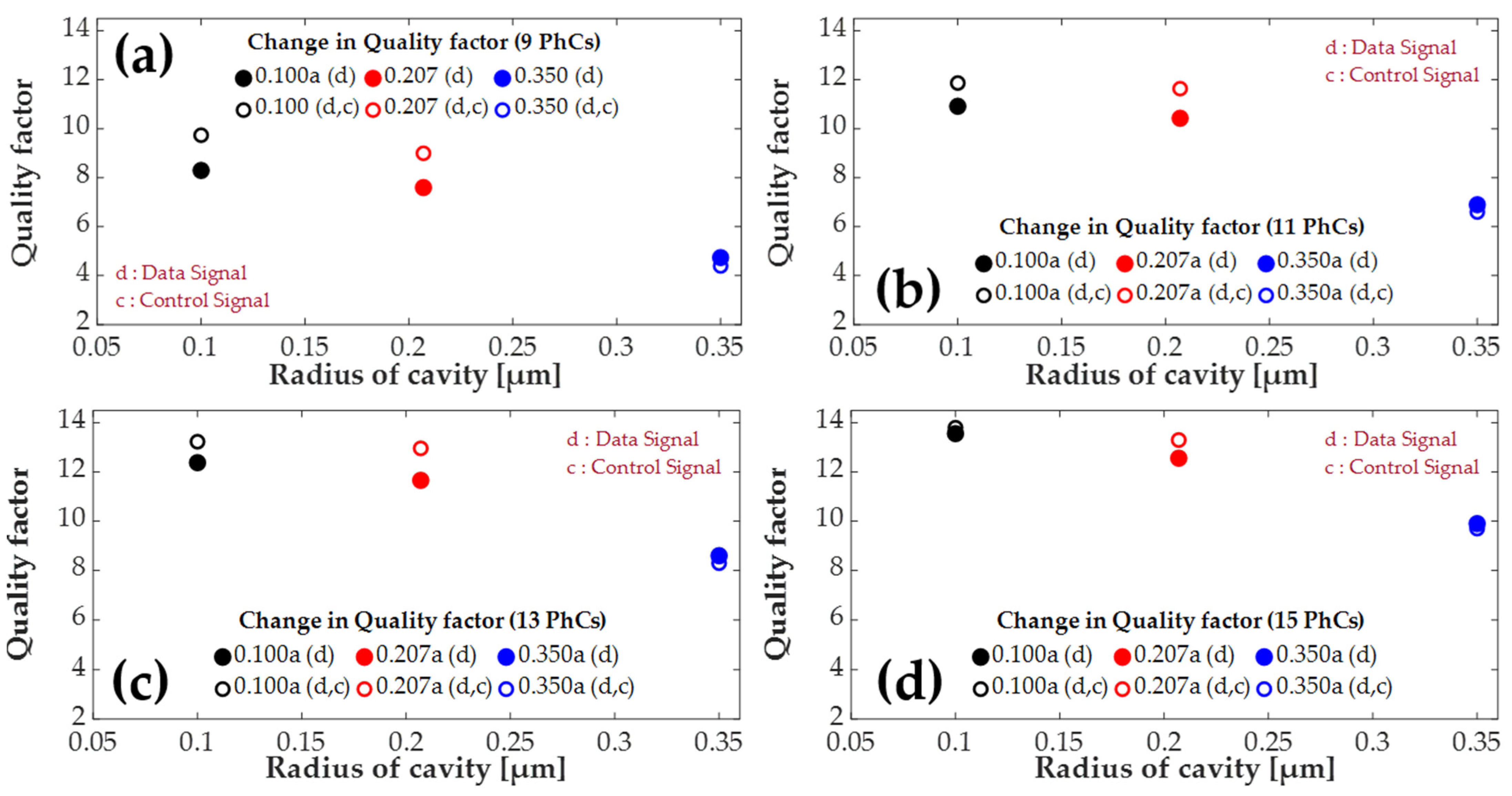
4.8. Comparative Analysis of Quality Factor against Variation in the Number of PhC Elements and Radius of PhC-Cavity for Optical Switching Action

| Radius of Cavity (9 PhCs) | Resonant Wavelength (µm) | Reflection Peaks (×100%) | Linewidth (µm) | |||
| Single Sour | Two Sources | Single Source | Two Sources | Single Source | Two Sources | |
| 0.100a | 1.55 | 1.551 | 0.706 | 0.779 | 0.0858 | 0.0799 |
| 0.207a | 1.546 | 1.546 | 0.695 | 0.755 | 0.0914 | 0.0836 |
| 0.350a | 1.556 | 1.549 | 0.5116 | 0.4806 | 0.1079 | 0.1090 |
| Radius of Cavity (11 PhCs) | Resonant Wavelength (µm) | Reflection Peaks (×100%) | Linewidth (µm) | |||
| Single Source | Two Sources | Single Source | Two Sources | Single Source | Two Sources | |
| 0.100a | 1.549 | 1.55 | 0.805 | 0.8677 | 0.0737 | 0.0731 |
| 0.207a | 1.545 | 1.545 | 0.8114 | 0.859 | 0.0778 | 0.0738 |
| 0.350a | 1.55 | 1.547 | 0.6419 | 0.614 | 0.0929 | 0.0937 |
| Radius of Cavity (13 PhCs) | Resonant Wavelength (µm) | Reflection Peaks (×100%) | Linewidth (µm) | |||
| Single Source | Two Sources | Single Source | Two Sources | Single Source | Two Sources | |
| 0.100a | 1.545 | 1.546 | 0.883 | 0.929 | 0.0713 | 0.0702 |
| 0.207a | 1.543 | 1.543 | 0.8678 | 0.9165 | 0.0744 | 0.0707 |
| 0.350a | 1.546 | 1.545 | 0.731 | 0.7107 | 0.0854 | 0.0854 |
| Radius of Cavity (15 PhCs) | Resonant Wavelength (µm) | Reflection Peaks (×100%) | Linewidth (µm) | |||
| Single Source | Two Sources | Single Source | Two Sources | Single Source | Two Sources | |
| 0.100a | 1.542 | 1.544 | 0.9518 | 0.9592 | 0.0701 | 0.0697 |
| 0.207a | 1.542 | 1.543 | 0.9112 | 0.9228 | 0.0725 | 0.0696 |
| 0.350a | 1.544 | 1.543 | 0.7985 | 0.7811 | 0.0809 | 0.0803 |
5. Discussion
6. Conclusions
Author Contributions
Funding
Data Availability Statement
Acknowledgments
Conflicts of Interest
References
- Wang, Y.; Yang, J.; Wang, Z.; Kong, X.; Sun, X.; Tian, J.; Zhang, X.; Zhao, X.; Liu, Y.; Li, H.; et al. The Development and Progression of Micro-Nano Optics. Front. Chem. 2022, 10, 916553. [Google Scholar] [CrossRef] [PubMed]
- Demkov, A.A.; Bajaj, C.; Ekerdt, J.G.; Palmstrøm, C.J.; Ben Yoo, S.J. Materials for Emergent Sili-con-Integrated Optical Computing. J. Appl. Phys. 2021, 130, 070907. [Google Scholar] [CrossRef] [PubMed]
- Bogaerts, W.; Pérez, D.; Capmany, J.; Miller, D.A.; Poon, J.; Englund, D.; Morichetti, F.; Melloni, A. Programmable Photonic Circuits. Nature 2020, 586, 207–216. [Google Scholar] [CrossRef] [PubMed]
- Ji, X.; Liu, J.; He, J.; Wang, R.N.; Qiu, Z.; Riemensberger, J.; Kippenberg, T.J. Compact, Spa-tial-Mode-Interaction-Free, Ultralow-Loss, Nonlinear Photonic Integrated Circuits. Commun. Phys. 2022, 5, 84. [Google Scholar] [CrossRef]
- Masilamani, S.; Punniakodi, S. Photonic Crystal Ring Resonator Based Optical MUX/DEMUX Design Structures: A Survey and Comparison Study. J. Opt. 2020, 49, 168–177. [Google Scholar] [CrossRef]
- Yanik, M.F.; Fan, S.; Soljačić, M.; Joannopoulos, J.D. All-optical transistor action with bistable switching in a photonic crystal cross-waveguide geometry. Opt. Lett. 2003, 28, 2506–2508. [Google Scholar] [CrossRef]
- Krishnamurthy, V.; Chen, Y.; Ho, S.-T. Photonic Transistor Design Principles for Switching Gain ≥ 2. J. Light. Technol. 2013, 31, 2086–2098. [Google Scholar] [CrossRef]
- Butt, M.; Khonina, S.; Kazanskiy, N. Recent advances in photonic crystal optical devices: A review. Opt. Laser Technol. 2021, 142, 107265. [Google Scholar] [CrossRef]
- Tavana, S.; Bahadori-Haghighi, S.; Sheikhi, M.H. High-performance electro-optical switch using an anisotropic graphene-based one-dimensional photonic crystal. Opt. Express 2022, 30, 9269. [Google Scholar] [CrossRef]
- Xu, H.; Lin, Z.; Dai, X. MoTe Quantum Dots-Based All-Optical Switching. Opt. Commun. 2022, 506, 127573. [Google Scholar] [CrossRef]
- Daghooghi, T.; Soroosh, M.; Ansari-Asl, K. Low-power all-optical switch based on slow light photonic crystal. Photonics Netw. Commun. 2022, 43, 177–184. [Google Scholar] [CrossRef]
- Khan, Y.; Rehman, A.U.; Batool, B.A.; Noor, M.; Butt, M.A.; Kazanskiy, N.L.; Khonina, S.N. Fabrication and Investigation of Spectral Properties of a Dielectric Slab Waveguide Photonic Crystal Based Fano-Filter. Crystals 2022, 12, 226. [Google Scholar] [CrossRef]
- Joannopoulos, J.D.; Villeneuve, P.R.; Fan, S. Photonic Crystals: Putting a new twist on Light: A Review. Nature 1997, 386, 143–149. [Google Scholar] [CrossRef]
- Hu, X.; Gong, Q.; Liu, Y.; Cheng, B.; Zhang, D. All-optical switching of defect mode in two-dimensional nonlinear organic photonic crystals. Appl. Phys. Lett. 2005, 87, 231111. [Google Scholar] [CrossRef]
- Khan, Y.; Butt, M.A.; Kazanskiy, N.L.; Khonina, S.N. Numerical Study of Fabrication-Related Effects of the Structural-Profile on the Performance of a Dielectric Photonic Crystal-Based Fluid Sensor. Materials 2022, 15, 3277. [Google Scholar] [CrossRef]
- Hu, X.; Jiang, P.; Ding, C.; Yang, H.; Gong, Q. Picosecond and low-power all-optical switching based on an organic photonic-bandgap microcavity. Nat. Photonics 2008, 2, 185–189. [Google Scholar] [CrossRef]
- Heuck, M.; Kristensen, P.T.; Elesin, Y.; Moerk, J. Improved switching using Fano resonances in photonic crystal structures. Opt. Lett. 2013, 38, 2466–2468. [Google Scholar] [CrossRef]
- Dong, H.M.; Bang, N.H.; Khoa, D.X.; Van Doai, L. All-optical switching via spontaneously generated coherence, relative phase and incoherent pumping in a V-type three-level system. Opt. Commun. 2021, 507, 127731. [Google Scholar] [CrossRef]
- Dhama, R.; Panahpour, A.; Pihlava, T.; Ghindani, D.; Caglayan, H. All-optical switching based on plasmon-induced Enhancement of Index of Refraction. Nat. Commun. 2022, 13, 3114. [Google Scholar] [CrossRef]
- Rebhi, S.; Najjar, M. Hourglass Nonlinear Photonic Crystal Cavity for Ultra-Fast All-Optical Switching. Optik 2018, 180, 858–865. [Google Scholar] [CrossRef]
- Belotti, M.; Galisteo-López, J.F.; De Angelis, S.; Galli, M.; Maksymov, I.; Andreani, L.C.; Peyrade, D.; Chen, Y. All-optical switching in 2D silicon photonic crystals with low loss waveguides and optical cavities. Opt. Express 2008, 16, 11624–11636. [Google Scholar] [CrossRef] [PubMed]
- Pezeshki, H.; Darvish, G. Design of photonic crystal microcavity based optical switches using Fano resonance effect. Optik 2015, 126, 4202–4205. [Google Scholar] [CrossRef]
- Zhou, H.; Qiu, C.; Jiang, X.; Zhu, Q.; He, Y.; Zhang, Y.; Su, Y.; Soref, R. Compact, submilliwatt, 2 × 2 silicon thermo-optic switch based on photonic crystal nanobeam cavities. Photonics Res. 2017, 5, 108–112. [Google Scholar] [CrossRef]
- Granpayeh, A.; Habibiyan, H.; Parvin, P. Photonic Crystal Directional Coupler for All-Optical Switching, Tunable Multi/Demultiplexing and Beam Splitting Applications. J. Mod. Opt. 2018, 66, 359–366. [Google Scholar] [CrossRef]
- Takiguchi, M.; Shinya, A.; Notomi, M.; Takemura, N.; Tateno, K.; Nozaki, K.; Sasaki, S.; Sergent, S.; Kuramochi, E.; Wasawo, T.; et al. All-Optical Switching using a III-V Nanowire Integrated Si Photonic Crystal Nanocavity. In Proceedings of the 2019 IEEE Photonics Conference (IPC), San Antonio, TX, USA, 29 September–3 October 2019; pp. 1–2. [Google Scholar] [CrossRef]
- Bekele, D.A.; Marchevsky, A.; Saudan, Q.; Yu, Y.; Galili, M.; Oxenlowe, L.K.; Yvind, K.; Mork, J. Towards High-Speed Fano Photonic Switches. In Proceedings of the 2019 21st International Conference on Transparent Optical Networks (ICTON), Angers, France, 9–13 July 2019; pp. 1–4. [Google Scholar] [CrossRef]
- Zhang, X.; Yang, J. Ultrafast Plasmonic Optical Switching Structures and Devices. Front. Phys. 2019, 7, 190. [Google Scholar] [CrossRef]
- Azizpour, M.R.J.; Soroosh, M.; Dalvand, N.; Seifi-Kavian, Y. All-Optical Ultra-Fast Graphene-Photonic Crystal Switch. Crystals 2019, 9, 461. [Google Scholar] [CrossRef]
- Rutckaia, V.; Schilling, J. Ultrafast low-energy all-optical switching. Nat. Photonics 2019, 14, 4–6. [Google Scholar] [CrossRef]
- Eid, M.M.; Rashed, A.N.Z. High speed optical switching gain based EDFA model with 30 Gb/s NRZ modulation code in optical systems. J. Opt. Commun. 2020, 1–6. [Google Scholar] [CrossRef]
- Kuttruff, J.; Garoli, D.; Allerbeck, J.; Krahne, R.; De Luca, A.; Brida, D.; Caligiuri, V.; Maccaferri, N. Ultrafast all-optical switching enabled by epsilon-near-zero-tailored absorption in metal-insulator nanocavities. Commun. Phys. 2020, 3, 114. [Google Scholar] [CrossRef]
- Nguyen, H.A.; Grange, T.; Malik, N.S.; Dupuy, E.; Tumanov, D.; de Assis, P.L.; Yeo, I.; Fratini, F.; Gregersen, N.; Auffèves, A.; et al. Ultra-Low Power Optical Transistor Using a Single Quantum Dot. In Proceedings of 2017 Conference on Lasers and Electro-Optics Europe & European Quantum Electronics Conference (CLEO/Europe-EQEC), Munich, Germany, 25–29 June 2017. [Google Scholar]
- Goodarzi, A.; Ghanaatshoar, M. Coherent all-optical transistor based on frustrated total internal reflection. Sci. Rep. 2018, 8, 5069. [Google Scholar] [CrossRef]
- Moradi, M.; Mohammadi, M.; Olyaee, S.; Seifouri, M. Design and Simulation of a Fast All-Optical Modulator Based on Photonic Crystal Using Ring Resonators. Silicon 2021, 14, 765–771. [Google Scholar] [CrossRef]
- Rani, P.; Kalra, Y.; Sinha, R. Design of all optical logic gates in photonic crystal waveguides. Optik 2015, 126, 950–955. [Google Scholar] [CrossRef]
- Goudarzi, K.; Mir, A.; Chaharmahali, I.; Goudarzi, D. All-optical XOR and OR logic gates based on line and point defects in 2-D photonic crystal. Opt. Laser Technol. 2016, 78, 139–142. [Google Scholar] [CrossRef]
- Younis, R.M.; Areed, N.F.F.; Obayya, S.S.A. Fully Integrated AND and OR Optical Logic Gates. IEEE Photonics Technol. Lett. 2014, 26, 1900–1903. [Google Scholar] [CrossRef]
- Mondal, H.; Goswami, K.; Sen, M.; Khan, W.R. Design and Analysis of All Optical Logic NOR Gate Based on Linear Optics. Opt. Quantum Electron. 2022, 272, 272. [Google Scholar] [CrossRef]
- Sharma, A.; Goswami, K.; Mondal, H.; Datta, T.; Sen, M. A review on photonic crystal based all-optical logic decoder: Linear and nonlinear perspectives. Opt. Quantum Electron. 2022, 54, 90. [Google Scholar] [CrossRef]
- Saudan, Q.; Bekele, D.A.; Dong, G.; Yu, Y.; Yvind, K.; Mørk, J.; Galili, M. Crosstalk-free all-optical switching enabled by Fano resonance in a multi-mode photonic crystal nanocavity. Opt. Express 2022, 30, 7457. [Google Scholar] [CrossRef]
- Khan, Y. Design and Numerical Simulation of Dielectric Photonic Crystal Devices and Investigation of an Optical Charac-terization Method. Ph.D Thesis, University of Kassel, Kassel, Germany, 2017. [Google Scholar]
- MEEP Tutorial. Available online: http://ab-initio.mit.edu/wiki/index.php/Meep_tutorial (accessed on 15 June 2022).
- Oskooi, A.F.; Roundy, D.; Ibanescu, M.; Bermel, P.; Joannopoulos, J.D.; Johnson, S.G. Meep: A Fexible Free-Software Package for Electromagnetic Simulations by the FDTD Method. Comput. Phys. Commun. 2010, 181, 687–702. [Google Scholar] [CrossRef]
- Kassa-Baghdouche, L. Optical properties of a point-defect nanocavity-based elliptical-hole photonic crystal for mid-infrared liquid sensing. Phys. Scr. 2019, 95, 015502. [Google Scholar] [CrossRef]
- Kassa-Baghdouche, L.; Boumaza, T.; Bouchemat, M. Optimization of Q-factor in nonlinear planar photonic crystal nanocavity incorporating hybrid silicon/polymer material. Phys. Scr. 2015, 90, 065504. [Google Scholar] [CrossRef]


| Parameters | Symbol | Value |
|---|---|---|
| Lattice constant | ||
| Radius of the PhC-elements | ||
| Thickness of waveguide | ||
| Thickness of cladding | - | |
| Refractive index of the substrate | ||
| Refractive index of the waveguide | - | |
| Resonant wavelength | ||
| Thickness of PML layer |
| Number of PhCs Periods | Single Source (Data Signal) | |||
|---|---|---|---|---|
| Reflection % | Finesse | Linewidth (µm) | FSR (µm) | |
| 09 PhC-elements | 60 | 6.08 | 0.073 | 0.444 |
| 11 PhC-elements | 70 | 8.763 | 0.07 | 0.613 |
| 13 PhC-elements | 71 | 9.129 | 0.066 | 0.603 |
| 15 PhC-elements | 79 | 13.298 | 0.061 | 0.811 |
Publisher’s Note: MDPI stays neutral with regard to jurisdictional claims in published maps and institutional affiliations. |
© 2022 by the authors. Licensee MDPI, Basel, Switzerland. This article is an open access article distributed under the terms and conditions of the Creative Commons Attribution (CC BY) license (https://creativecommons.org/licenses/by/4.0/).
Share and Cite
Rehman, A.U.; Khan, Y.; Irfan, M.; Butt, M.A.; Khonina, S.N.; Kazanskiy, N.L. A Novel Design of Optical Switch Based on Guided Mode Resonances in Dielectric Photonic Crystal Structures. Photonics 2022, 9, 580. https://doi.org/10.3390/photonics9080580
Rehman AU, Khan Y, Irfan M, Butt MA, Khonina SN, Kazanskiy NL. A Novel Design of Optical Switch Based on Guided Mode Resonances in Dielectric Photonic Crystal Structures. Photonics. 2022; 9(8):580. https://doi.org/10.3390/photonics9080580
Chicago/Turabian StyleRehman, Atiq Ur, Yousuf Khan, Muhammad Irfan, Muhammad A. Butt, Svetlana N. Khonina, and Nikolay L. Kazanskiy. 2022. "A Novel Design of Optical Switch Based on Guided Mode Resonances in Dielectric Photonic Crystal Structures" Photonics 9, no. 8: 580. https://doi.org/10.3390/photonics9080580
APA StyleRehman, A. U., Khan, Y., Irfan, M., Butt, M. A., Khonina, S. N., & Kazanskiy, N. L. (2022). A Novel Design of Optical Switch Based on Guided Mode Resonances in Dielectric Photonic Crystal Structures. Photonics, 9(8), 580. https://doi.org/10.3390/photonics9080580