Article

Ultra-Low-Loss and Broadband All-Silicon Dielectric Waveguides for WR-1 Band (0.75–1.1 THz) Modules

Graduate School of Engineering Sciences, Osaka University, Toyonaka City 560-8531, Japan
*
Authors to whom correspondence should be addressed.
Photonics 2022, 9(8), 515; https://doi.org/10.3390/photonics9080515
Submission received: 28 June 2022 / Revised: 18 July 2022 / Accepted: 21 July 2022 / Published: 24 July 2022
(This article belongs to the Special Issue Terahertz (THz) Science in Advanced Materials, Devices and Systems)

Abstract

:
This study presents ultra-low-loss and broadband all-silicon dielectric waveguides for the WR-1 band (0.75–1.1 THz). The waveguides are built in high-resistivity silicon (10 kΩ-cm) and integrated with supportive frames fabricated from the same silicon wafer in a single etch process to achieve a compact design. We pursued low-loss, broadband, substrateless, unclad and effective medium waveguides. Smaller propagation losses of 0.3 dB/cm and 0.1 dB/cm were achieved for the unclad and effective medium waveguides, respectively. The 3 dB bandwidth was not encountered in the frequency range of interest and was as broad as 350 GHz. An unclad waveguide was employed to devise a Y-junction to demonstrate its practical applications in terahertz imaging. An integrated circuit card was successfully scanned. In addition, we developed unclad waveguide, effective medium waveguide, and Y-junction modules. The modules incorporated an input/output interface compatible with a standard WR-1 flange (254 μm × 127 μm). Unlike the conventional hollow waveguide modules, the unclad waveguide and effective medium waveguide modules reported total loss improvements of 6 dB and 8 dB, respectively, across the operation band. Our results provided a systematic way of achieving low-loss, compact, and versatile modules in the WR-1 band based on all-dielectric-waveguide platforms.

1. Introduction

The terahertz (THz) range has recently attracted a lot of interest among researchers, with a substantial amount of research effort being dedicated to exploring the frequencies from 100 GHz to 10 THz that are covered by the terahertz range. Recent efforts have been accelerated by nanophotonics [1], which have enabled a broad range of applications, including high-data-rate wireless communications [2] and high-resolution imaging [3]. Until recently, existing systems were designed to operate in the lower end of the terahertz band, spanning frequencies up to 0.3 THz [4] and 0.6 THz [5]. This has restricted the assessment of the full potential of the THz range. The development of more sophisticated and capable THz systems requires current research to focus on higher frequencies targeting the frequencies in the WR-1 band (0.75–1.1 THz). These ultrahigh frequencies could contribute to accelerating future applications such as space exploration [6], non-invasive and non-destructive super-resolution imaging [7,8], sensing [9,10], and ultrafast wireless communications [11]. At higher frequencies, higher data rates can be achieved owing to increased bandwidth [12]. Indeed, higher frequencies lead to higher channel capacities, as stated by Shannon’s theorem. Hence, data rates as high as one terabits/s in wireless communications can be achievable [13]. A noticeable advantage of higher frequencies for THz components and systems built on all-silicon (Si) materials is the reduction in the propagation loss determined by the absorption loss of the Si material. With increase in frequency, the absorption loss due to free carriers in Si decreases [14]. A few issues still remain unaddressed in terms of taking advantage of the THz range. The lack of high-power sources and high-sensitivity detectors at high frequencies is a noticeable hindrance. For instance, the output power of commercially available signal generators decreases from ~5 dBm at 0.3 THz to −23 dBm at 1 THz; the sensitivity of a zero bias diode decreases from ~1.8 V/W at 0.3 THz to 0.75 V/W at 1 THz [1] because of the inherent difficulty in generating THz waves with artificial sources [15]. It is desirable to seek efficient integration with diverse components and sources to compensate for the decrease in available power, which will require THz-range interconnects.
Waveguides are fundamental components in electronics that can serve as interconnects with external power sources, signal probers, and various components essential for the generation and manipulation of THz waves. Hollow waveguides have become standard owing to extensive research on metallic rectangular and circular waveguides in the microwave region, where they yield good performance. These waveguides rely on guided waves based on the metallic media principle; that is, the waves are confined within the metallic walls of the waveguides. Hollow metallic waveguides have been the preferred interconnects in the THz range. However, at THz frequencies, the ohmic loss associated with the metal increases. In addition, metallic hollow waveguides are unsuitable to integrate with most THz-range components that are made of thin planar Si because of their non-planar profile as well as their relatively large physical size compared to the wavelength in the THz range. In addition, metal-based interconnects such as hollow waveguides have led to THz systems that are bulky, with numerous individual components that exacerbate insertion and ohmic losses.
Meanwhile, the development of low-loss THz-range waveguides has been accelerated by the progress in Nanophotonics. All-Si waveguide platforms are current focus of research because they have reported losses as low as 0.1 dB/cm owing to the low absorption loss of high-resistivity Si material. Various all-Si waveguides exist depending on the technology employed for their implementation. Photonic crystal waveguides are fundamental components built by perforating an array of through-holes into a silicon slab. These waveguides rely on the photonic bandgap effect to confine a THz wave in the waveguide track and achieve a reported low loss <0.1 dB/cm [16,17,18]. Photonic crystal waveguides have enabled many applications, including hybrid integration with active components [4,19,20] and the realization of efficient communication links employing THz fibers with achieved data rates of 10 Gbps at 0.33 THz [21]. However, these waveguides suffer from a limited bandwidth of approximately 20 GHz [16]. Subsequent to the photonic crystal waveguides, effective medium (EM) waveguides were implemented based on the effective-medium principle. EM waveguides have reported low loss and a broader bandwidth of >120 GHz [22], enabling novel applications in high-data-rate wireless communications. Despite the increased bandwidth, EM waveguides are difficult to implement because of the small size and high density of holes. More recent waveguides have further reduced waveguide loss while maintaining the broader bandwidth of effective medium waveguides [22] by excavating a portion of the effective medium section of the waveguide, leaving only the waveguide track [23]. These are unclad waveguides and they have reported extremely low losses, and have recently been employed for novel applications in hybrid integration and terahertz-range communications. Another advantage of the unclad waveguides is their versatility. Indeed, essential components, such as bends and splits, can be easily implemented using unclad waveguides with very little loss [23].
In this study, we propose ultra-low-loss and broadband unclad and EM dielectric waveguide interconnects for the WR-1 band, covering THz frequencies in 0.75–1.1 THz. The proposed waveguides were used to implement a packaged, unclad waveguide module and an EM waveguide module with an input/output (I/O) interface compatible with a standard WR-1 flange. In addition, we have developed a Y-junction based on an unclad waveguide to demonstrate THz imaging applications.

2. Materials and Method—All-Si Dielectric Waveguides
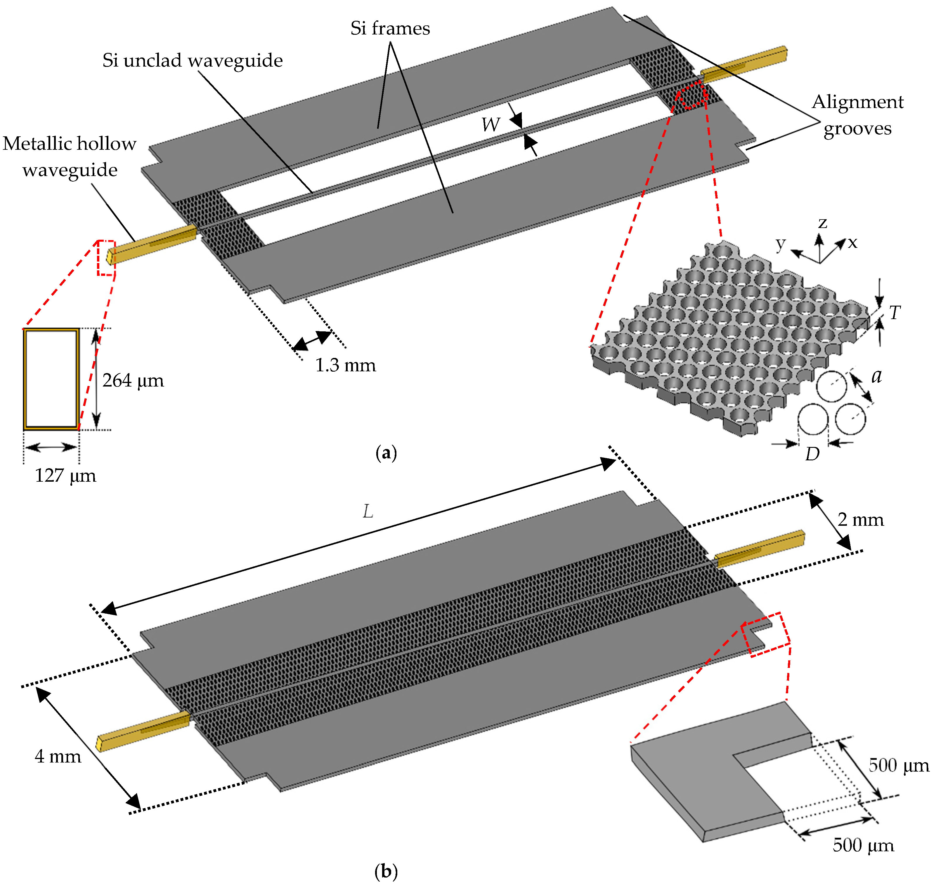
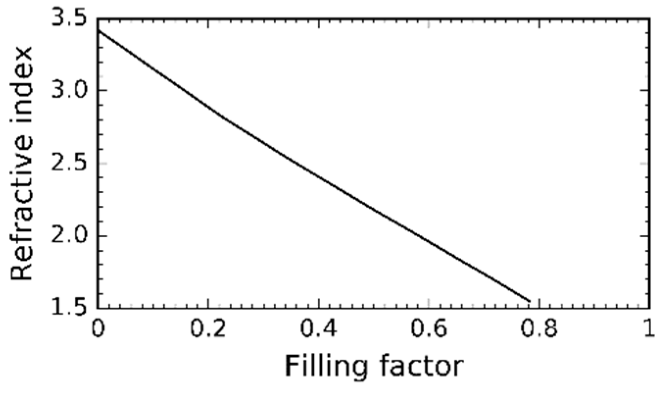
2.1. Design

Figure 1a,b shows the designs of the unclad waveguide and the EM waveguide, respectively. Both waveguides proposed in this study rely on EM theory, which allows for the engineering of novel materials whose properties are inherited from the constituent composite materials. The EM waveguide has two main sections: the waveguide core and the EM section. The EM section was realized by introducing an array of through-holes in an 80 μm-thick silicon slab with a relative permittivity ε S i of 11.68, which corresponds to a refractive index of 3.418 and a resistivity of >10 kΩ-cm. The holes have a diameter D = 35 μm and were perforated following an equilateral lattice with a period a = 45 μm. Introducing the array of through-holes makes it possible to obtain a novel material with a refractive index between that of intrinsic silicon and that of air. The resulting refractive index is strongly dependent on a and D, and the values of a and D were obtained after a careful parameter sweep on these values. The waveguide core is therefore cladded in-plane by the EM section and out-of-plane by air, creating an index contrast between the waveguide core and cladding, which can be confined by total internal reflection (TIR). Consequently, the waveguides support a transverse electric (TE) mode that is parallel to the slab. This mode is associated with an in-plane electric field in which the relative permittivity can be approximated using Maxwell–Garnett approximations following the equation [24]:
ε x = ε S i ( ε 0 + ε S i ) + ( ε 0 ε S i ) ζ ( ε 0 + ε S i ) ( ε 0 ε S i ) ζ
where ε 0 and ε S i are the permittivities of air and Si, respectively, and ζ represents the filling factor of the air in silicon.
The unclad waveguide is built upon the EM waveguide owing to the difficulty associated with the fabrication of EM waveguides. Owing to the small size of the holes, higher-precision machining is required to manufacture subwavelength hole diameters. This motivated the removal, or at least the reduction in the cladding section with small holes, to achieve substrateless designs that are entirely cladded by air. This allows for a simpler design with reduced complexity and ease of fabrication. Nevertheless, for ease of handling and practicality, a small portion of EM cladding was maintained. The EM section of the unclad waveguide is identical to that of the EM waveguides, that is, a = 45 μm and D = 35 μm. The waveguides were also built on 80 μm-thick high-resistivity intrinsic silicon. Both the EM and unclad waveguides have an EM section that is 1.3 mm-long in the case of the unclad waveguide, and a length of L that corresponds to the length of the entire waveguide in the case of the EM waveguide. In both cases, the EM section is 2 mm-wide. For both waveguides, the waveguide core is 100 μm-wide and of thickness 80 μm. Frames are implemented in both waveguides for practicality and ease of handling, as well as to facilitate integration with metallic packaging. Alignment grooves of 0.5 × 0.5 mm2 are implemented into the frames to help align the waveguides within the metal packaging. Each frame is 1.5 mm wide, which renders the total width of each waveguide to 5 mm. The waveguides are terminated at both ends with 1.2 mm-long linear tapers. The waveguides were evaluated by a three-dimensional finite-integral time-domain electromagnetic simulation (CST Studio Suite 2021), and the electric field distributions at the center frequency of the WR-1 band (0.925 THz) are shown in Figure 2a,b for the unclad waveguide and EM waveguide, respectively. The electric-field distributions reveal strong confinement of THz waves within the waveguide core.
The waveguides previously reported for the WR-2.8 band (0.26–0.39 THz) achieved good performance, with hole pitches of 100 μm and 120 μm, as reported in [22,23], respectively, while maintaining a minimum manufacturable limitation of 10 μm for hole diameters of 90 μm and 110 μm, respectively. Following a simple scaling of [22,23] to (0.75–1.1 THz) would render a hole pitch of ~35.7 μm and ~42.8 μm, respectively; the scaling hole diameter would be 32.1 μm and 39.2 μm. This would lead to 3.2 μm and 3.6 μm clearance between two consecutive holes. However, such small distances are not manufacturable. Therefore, additional considerations were made to increase the minimum distance between two adjacent holes. This could be achieved by decreasing the refractive index. The EM theory requires that the hole pitch should be chosen to be smaller than the quarter wavelength in the EM. Given that the minimum wavelength in WR-1 is ~270 μm, the quarter wavelength in EM is ~20 μm at 1.1 THz with a refractive index of 3.418. Choosing the correct values of D and a will help in changing the refractive index, as D and a define the filling factor. According to Equation (1), the refractive index decreases with the filling factor, as illustrated in Figure 3. For example, a refractive index of 2, which corresponds to D = 35 μm and a = 45 μm, would yield a quarter wavelength in EM ~35 μm. This should satisfy the minimum manufacturability condition. However, considering air cladding in the plane perpendicular to the waveguide, the 3D index should be further reduced. A study of the waveguide performance for different values of W and T, as shown in Figure 4, revealed that the waveguide width W has a larger impact on the improvement of the transmittance. Figure 4a,b show that the thickness of the waveguide has no impact on the transmittance, whereas Figure 4c reveals that the transmittance is improved from ~1 dB at 0.75 THz when the waveguide width is increased from 80 μm to 100 μm for the unclad waveguide. Figure 4d reveals similar improvement of ~1 dB at 0.75 THz.

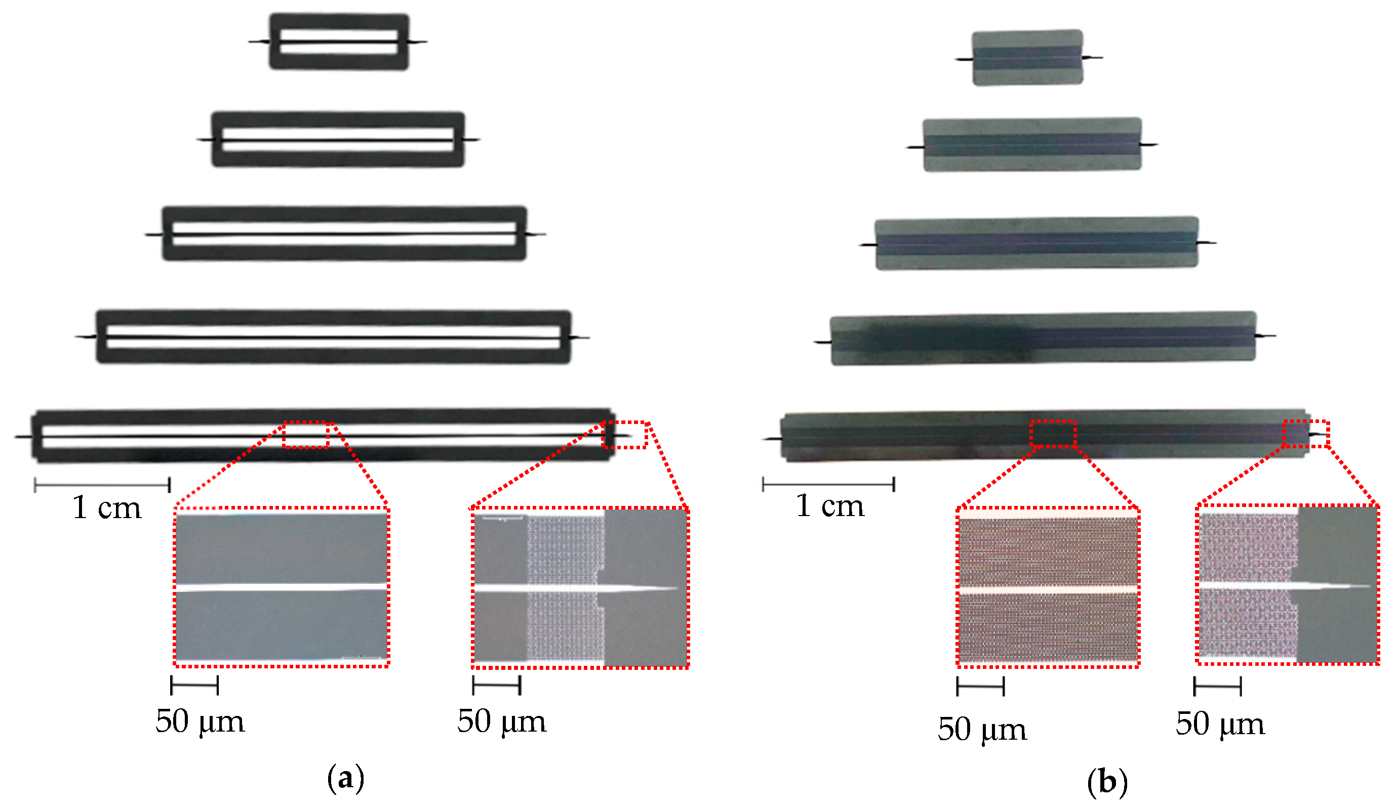
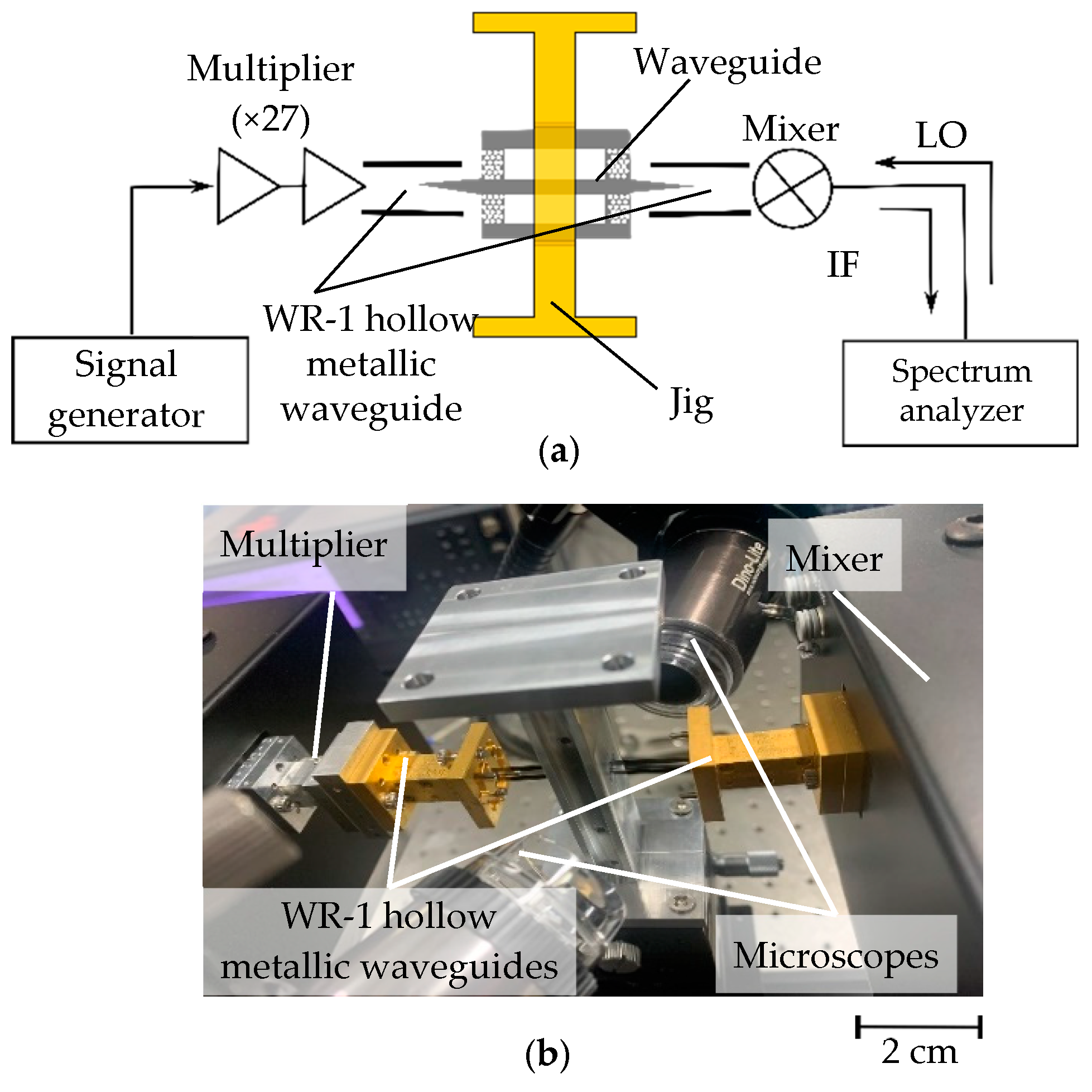
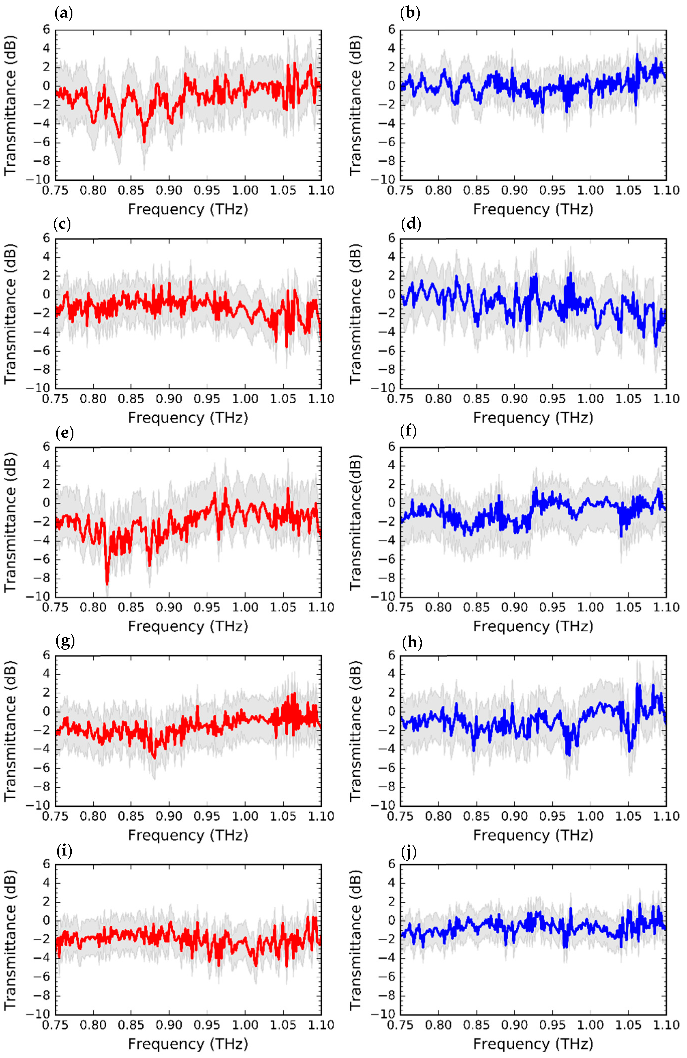
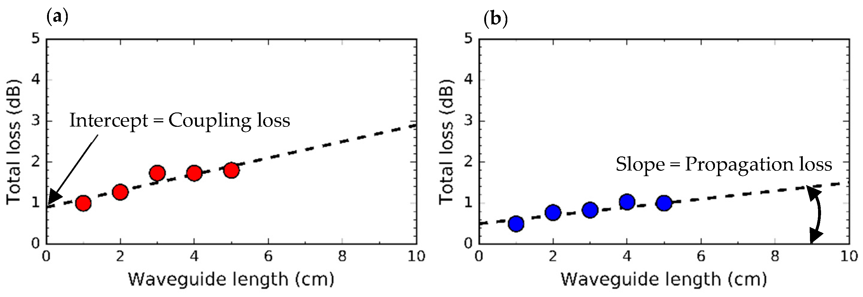
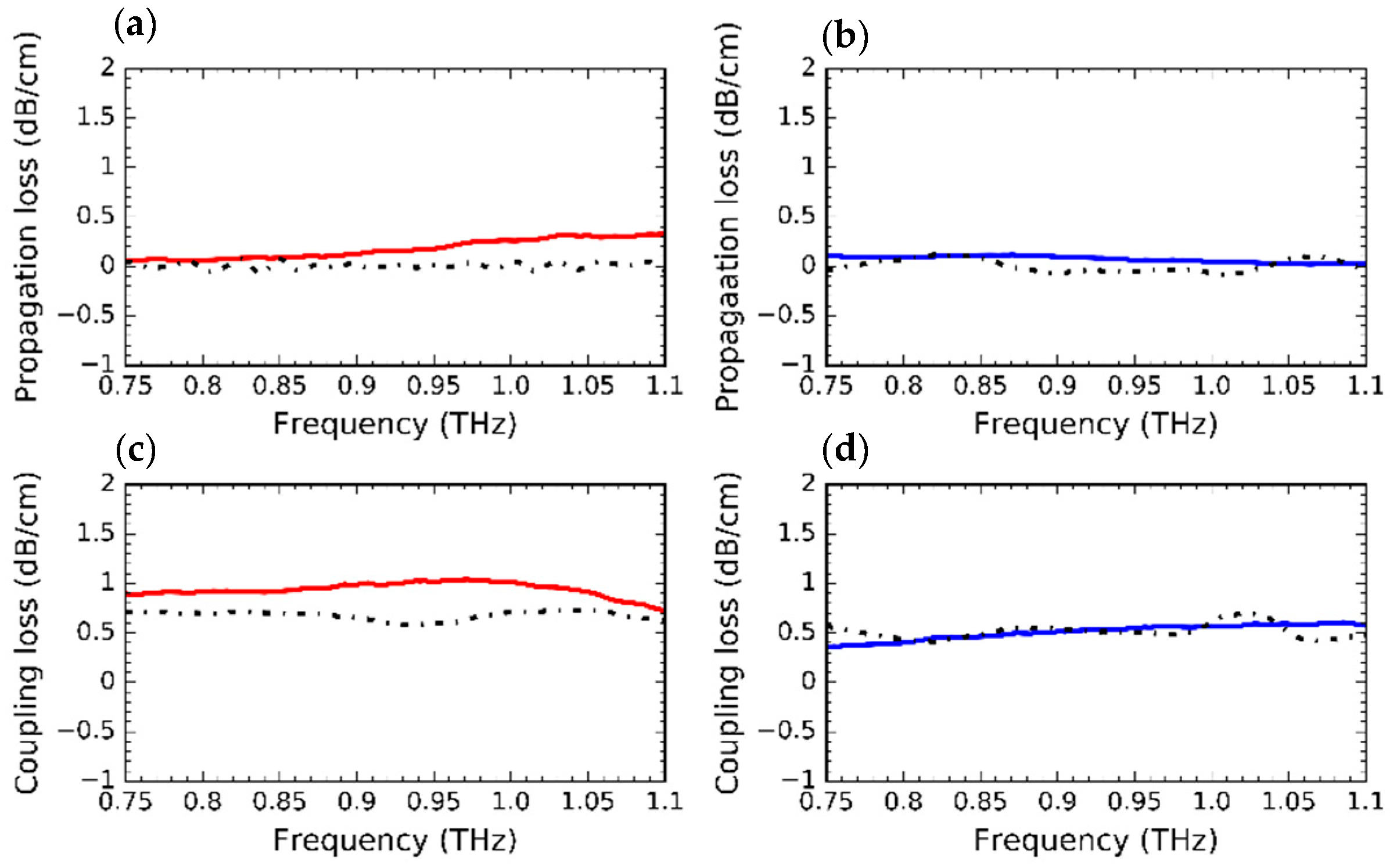
2.2. Fabrication and Experimental Validation

We fabricated unclad and EM waveguides with different lengths L (1, 2, 3, 4, and 5 cm). For the fabrication of the waveguides, we prepared an 80 μm-thick, 4-inch float-zone silicon wafer with the resistivity >10 kΩ∙cm. The samples were fabricated by photolithography and deep reactive ion etching (DRIE) using the manufacturing process of microelectromechanical systems foundry with a minimum guaranteed dimension of 10 microns. The resulting unclad and EM waveguides are shown in Figure 5a and 5b, respectively. Micrographs are shown to highlight key sailing features such as EM sections and coupling linear tapers.
We measured the power transmission of these waveguides using the experimental setup shown in Figure 6. As shown in Figure 6a, the power transmission was probed by inserting linear tapers of the waveguides into metallic hollow waveguides. For the WR-1 band, the physical dimensions of the rectangular hollow waveguide are 127 μm × 254 μm, which targets the frequencies in 0.75–1.1 THz. The small dimensions of this waveguide can hinder accurate measurements in experiments and may pose a challenge in general for higher frequencies. To overcome this issue, we employed commercially available microscopes (DINO Lite), as shown in Figure 6b, to obtain a better view of the opening of the metallic hollow waveguides for the insertion of Si tapers. In addition, we have devised supporting jigs to help position the waveguide devices, assuring vertical alignment and 0-tilt, which has helped reduce imperfect alignment, the main cause of coupling losses. The metallic hollow waveguides interface with commercially available signal generators coupled with a multiplier to deliver THz signals in the 0.75–1.1 THz range; that is, the signal generator delivers millimeter waves into a 27-times multiplier which in turn delivers the THz waves into the waveguides. A THz-range mixer was employed at the detection side to perform frequency down-conversion, producing microwave signals that were then processed by a spectrum analyzer.
Figure 7 shows the measured transmittances for the unclad (red) and EM (blue) waveguides. Each waveguide was measured five times, and for each measurement, the linear taper of the waveguide was removed from the hollow metallic waveguide on both the transmitter and receiver sides and then re-inserted. The standard deviation is used to derive error bars, which indicate the extent to which each measurement data point differs from the overall average. The error bar suggests minor differences between each measurement, which could be attributed to the positioning jigs that help secure the position of each sample between consecutive measurements. A shift in transmittance can be observed in both designs as the length of the waveguides, L, changes. For the unclad waveguides, the transmittance is shifted from a minimum of −5 dB—Figure 7i—for the longest waveguide (5 cm) to 0 dB—Figure 7a—for the shortest (1 cm). In the case of EM waveguides, the power transmission was found to be ~1 dB better than that of unclad waveguides. Specifically, the transmittance shifted from 4 dB (Figure 7j) for the longest waveguide (5 cm) to ~0 dB (Figure 7b) for the shortest (1 cm). In some cases, the transmittance was found to be >0 dB, which means that the power transmission is better when employing all-Si waveguides than when probing the reference measurement employing hollow metallic waveguides. This phenomenon has been observed previously in dielectric waveguides of this type in the WR2.8 band, and this phenomenon can be exacerbated in the WR-1 band [23]. However, this phenomenon can be possibly mitigated by averaging the measurements to derive the propagation and coupling losses.
We probed five waveguides of different lengths for both the unclad and EM designs to derive propagation and coupling losses using the difference in power transmission. Specifically, the transmittance for each waveguide length was plotted as a function of the frequency. Thereafter, for each frequency point, the transmittance data points were fitted to a curve using the least-squares method. The slope and intercept of the resulting curve are then used to estimate the propagation and coupling losses; that is, the propagation loss per unit length corresponds to the slope of the curve and the coupling loss to the Y-intercept. The deduction of the propagation and coupling losses is illustrated in Figure 8a,b for the unclad and EM waveguides, respectively.
Figure 9 shows the measured and simulated propagation losses for both the unclad waveguides (red) and effective-medium waveguides (blue). For the unclad waveguides, the simulated and measured propagation losses were in good agreement for the lower frequencies of up to ~0.9 THz. For the frequencies >0.9 THz, the measured propagation loss was found to be ~0.3 dB on average higher than simulated propagation loss. The results are shown in Figure 9a. This could be attributed to the difference in silicon properties and the limitations of the fabrication foundries. The propagation loss of the EM waveguide is presented in Figure 9b, and the measured and simulated losses are observed to be in good agreement. The coupling loss of the unclad waveguide is shown in Figure 9c. The measured coupling loss was greater than the simulated coupling loss. The difference is negligible for lower frequencies up to 0.8 THz and higher frequencies >1.05 THz with a difference of ~0.2 dB. The difference in coupling is exacerbated around the center frequency of 0.925 THz, reaching ~0.4 dB as opposed to the good agreement for the EM waveguide, as shown in Figure 9d. This can be ascribed to the coupling losses at different interfaces of the unclad waveguide. Indeed, both the unclad and EM waveguides have linear tapers that serve as coupling interfaces with the metallic hollow waveguides, but the unclad waveguide has additional interfaces at the point where the EM section is interrupted, revealing the waveguide core as a single wire. This transition from EM to air creates an additional coupling loss at both ends of the waveguide, which can be higher for the fabricated samples depending on the fabrication accuracy. With a difference in coupling loss of ~0.4 dB, we can attribute a ~0.2 dB loss to each EM-unclad transition interface. In addition, the results revealed the very broadband performance of these waveguides, as the 3-dB bandwidth was not encountered in the entire frequency range of interest, suggesting a bandwidth of ~350 GHz.

3. All-Silicon Dielectric Waveguide Modules
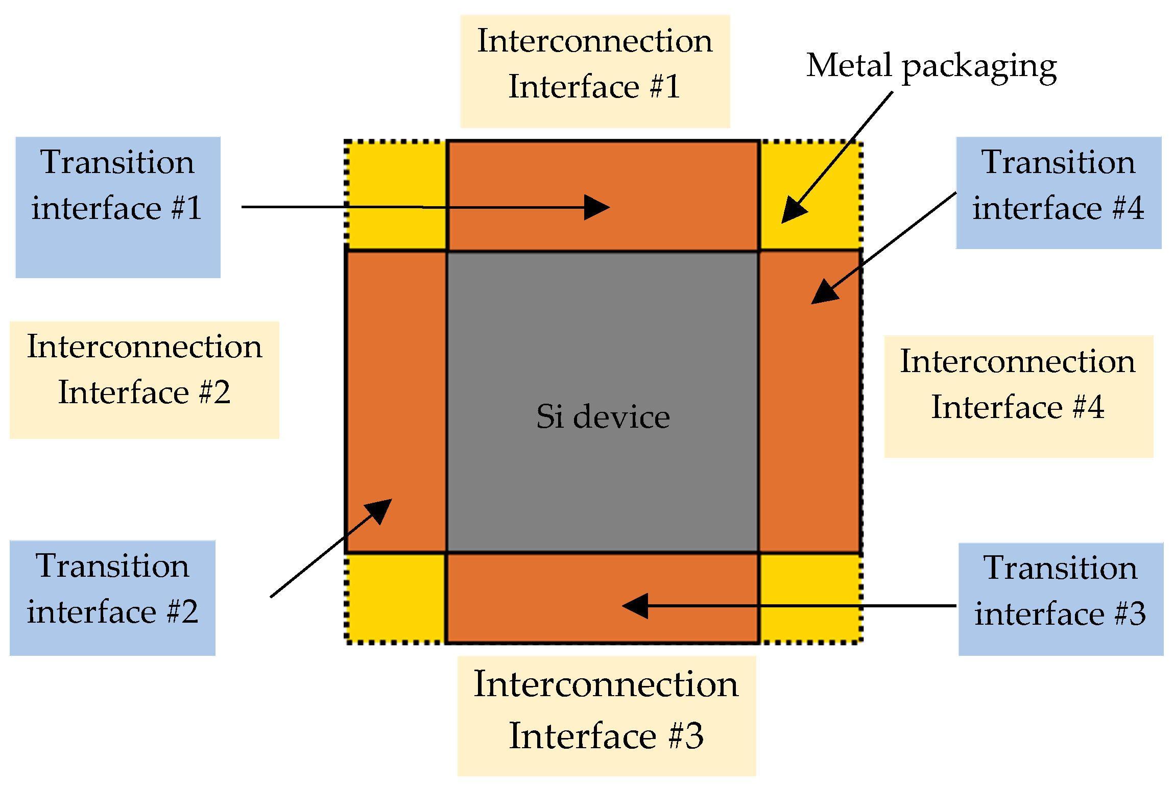
3.1. Concept

The main concept of the proposed modules is illustrated in Figure 10. An all-Si device that operates as the central component was encapsulated in metallic packaging. The Si device is terminated by transition interfaces that serve as interfaces with metallic packaging while ensuring a low insertion loss.
The transition interface also serves to secure the device onto packaging, ensuring safety and perfect alignment. Transition interfaces play a crucial role in reducing the impact of metallic packaging on the inherent behavior of the device. In practice, transition interfaces can be realized by employing photonic crystals [25] and effective mediums [26], as well as by gradual hole density [27]. Either technique can be considered while considering various performance indices of the waveguide, such as reflection, bandwidth, and fabrication limitations on the minimal manufacturable hole size. Transition interfaces usually incorporate all-Si tapered structures for smooth transitions. Among various taper shapes, linear tapers have proven to allow for the gradual transmission of THz waves with <0.2 dB coupling loss of [17] in the WR-2.8 band. For the WR-1 band, simulated coupling efficiency was found to be as high as >90% with <0.2 dB coupling loss. Linear tapers can also be implemented with a specific hole arrangement to improve matching at the interface where the taper contacts other THz-range components [28]. The transition interfaces are, in turn, terminated by interconnection interfaces that serve to interconnect the module with other terahertz-range components such as THz sources and detectors. In this study, the interconnection interface was an I/O interface compatible with the WR-1 standard flange.

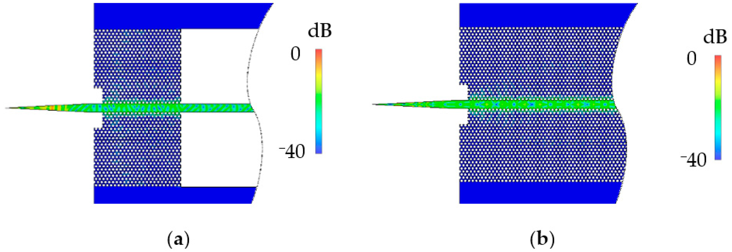
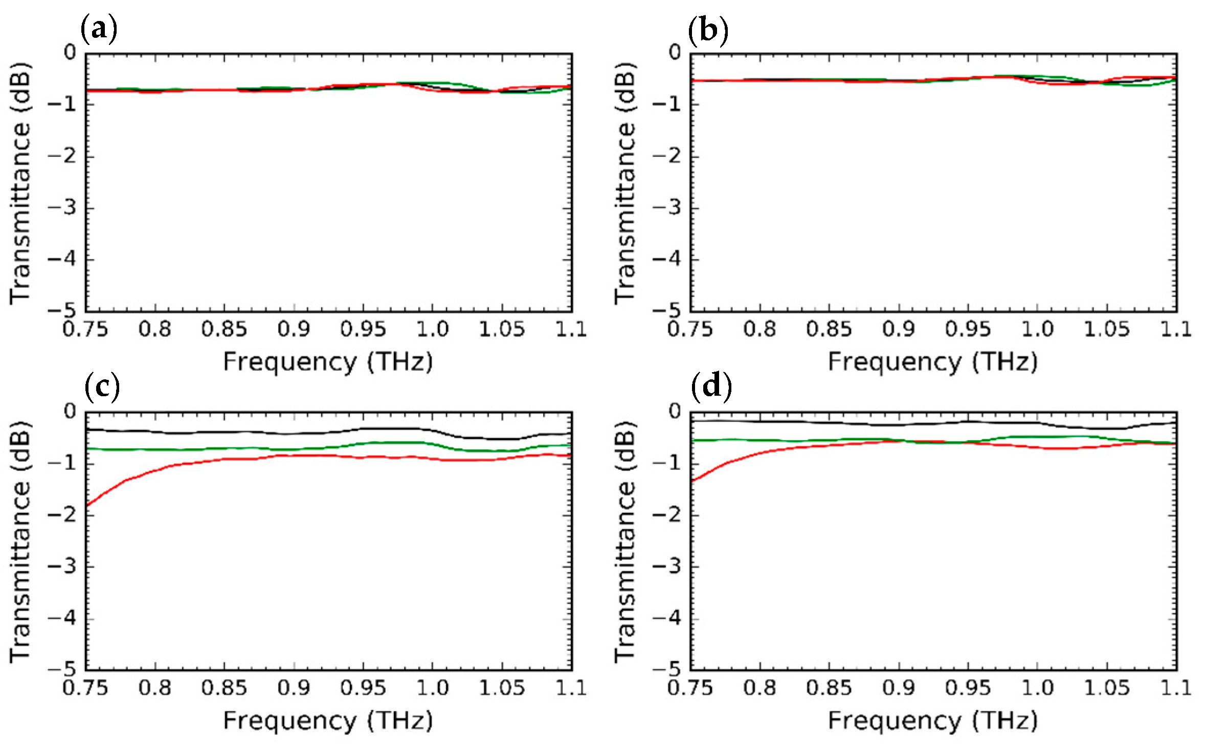
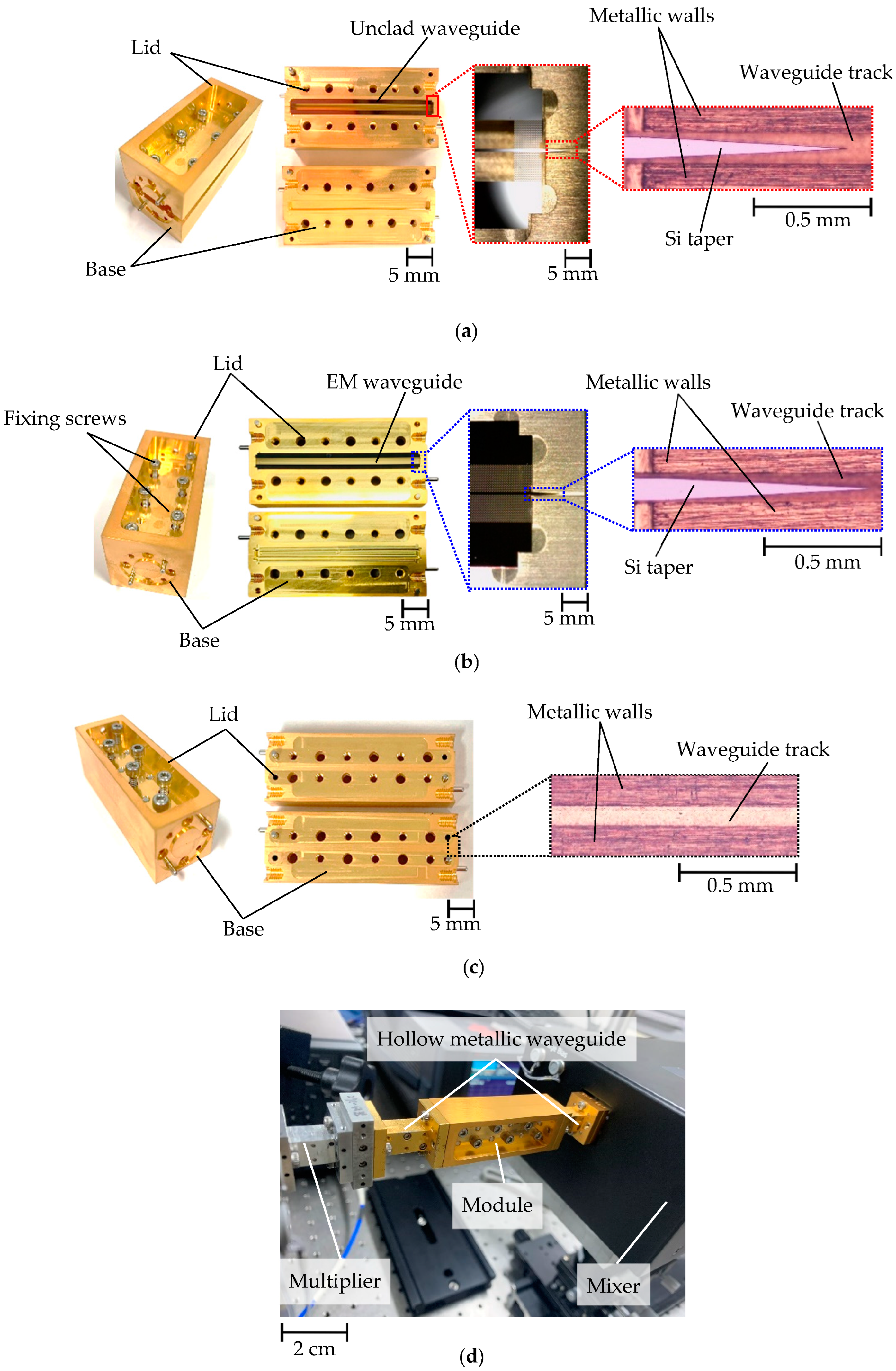
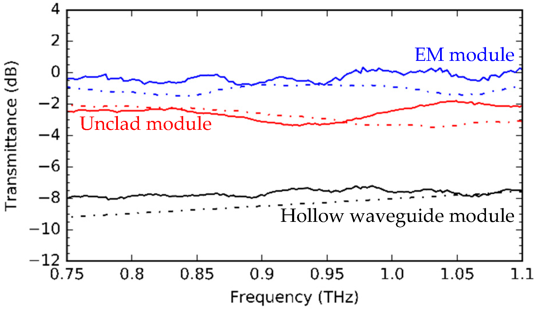
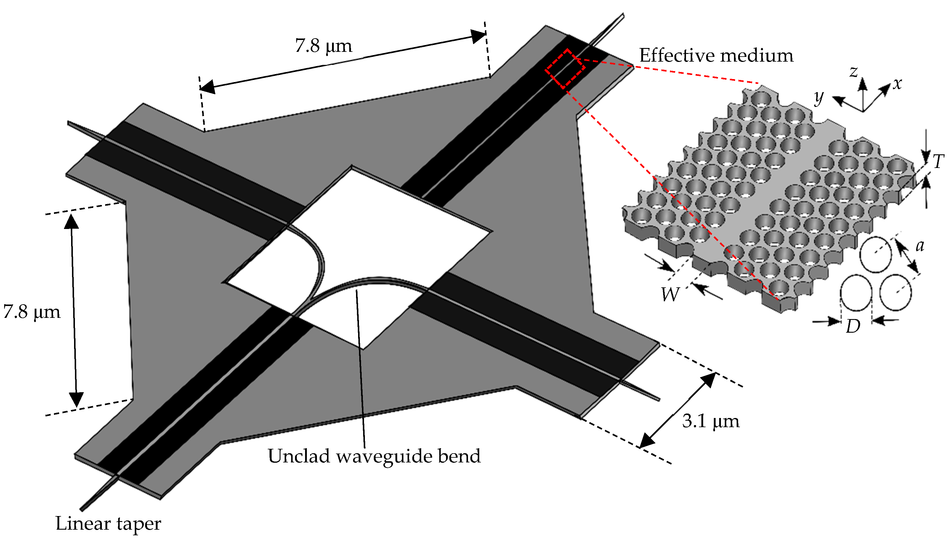
3.2. Unclad Waveguide and Effective-Medium Waveguide Modules

The modules were realized by devising metallic packaging to house the unclad and EM waveguides, as shown in Figure 1. Metallic packaging has an I/O interface that is compatible with the WR-1 standard hollow waveguide. The design of the module is illustrated in Figure 11. The packing is 56.2 mm × 26.0 mm × 26.0 mm and is made of copper with gold plating. The module comprises a base and a lid. A 2.3 mm-deep trench was carved out of the base, leaving a void wide enough to prevent the packing from impacting the inherent function of the waveguide core. The base was also designed to house the waveguide while ensuring perfect alignment with the integrated WR-1 hollow waveguide track. This was achieved by incorporating a shelf into the base on which the waveguide rested. The shelf had a depth of 40 μm, which is half the thickness of the waveguide.
This is because the lid is identical to the base; therefore, there is a 40 μm shelf in the lid as well. The width of the shelf matched that of the waveguides, including the frames, and was 5 mm. The modules also incorporate knobs that match the alignment grooves of the waveguide, thereby helping to fix the waveguide inside the module. For the assembly, each waveguide was carefully placed on the base such that the tapers sat in the hollow waveguide section of the metallic packaging. This is achieved by employing high-resolution microscopes to improve alignment accuracy. Employing microscopes was necessary because the dimensions in this band are extremely small. Once the waveguide was secured to the base, the lid was affixed with screws. The resulting module is extremely compact, lightweight, and can easily be connected to other terahertz-range components via the WR-1 band I/O interface, using screws to ensure perfect alignment, which is crucial for reducing insertion loss. We devised two metallic packaging and assembled an unclad waveguide module and an EM waveguide module, as shown in Figure 11a and Figure 11b, respectively. Micrographs are also shown, and it can be seen that the knobs of the base fit perfectly into the grooves of the waveguides. Additional micrographs are presented to show the positioning of the linear tapers within WR-1 standard hollow metallic waveguides. We also devised a 5 cm-long standard hollow metallic waveguide module, as shown in Figure 11c, to investigate its performance in comparison with the unclad waveguide module and EM waveguide module.
The power transmission of the three modules was probed using a similar system, as shown in Figure 6. A photograph of the experimental setup is shown in Figure 11d. Figure 12 shows the simulated (dashed line) and measured (solid line) transmittances of the modules. The transmittance of the unclad waveguide module is shown in red, that of the EM waveguide module in blue, and that of the metallic hollow waveguide in black. The measured and simulated transmittances of the EM waveguide module are in good agreement. In the case of the unclad waveguide module, the measured transmittance was in good agreement with the simulated transmittance for frequencies up to 0.95 THz. The transmittance is ~−2 dB for both simulated and measured across 0.75–1.1 THz. For frequencies >0.95 THz, the difference between the measured transmittance and simulated transmittance increases from 0 dB at ~0.955 THz to a maximum of ~0.8 dB at 1.05 THz, and finally, a 0.4 dB difference at 1.1 THz. For the hollow waveguide module, the trends of both simulated and measured transmittance are the same, with a performance difference of 0.4 dB at 0.75 THz, which slowly decreases to 0 dB at ~1.0 THz.
Probing the power transmission of these modules yielded results that were very close to the theoretical approximations. The unclad module has a ~6 dB loss improvement over the hollow waveguide module and a ~2 dB loss compared to the EM module. As discussed previously, this is due to the increased coupling loss of the unclad waveguide at the interface where the EM section is interrupted. The EM waveguide module has very little loss and exhibits a ~8 dB loss improvement over the hollow waveguide module. Both the unclad waveguide module and EM waveguide module demonstrate superior performance compared to the metallic hollow waveguide module.

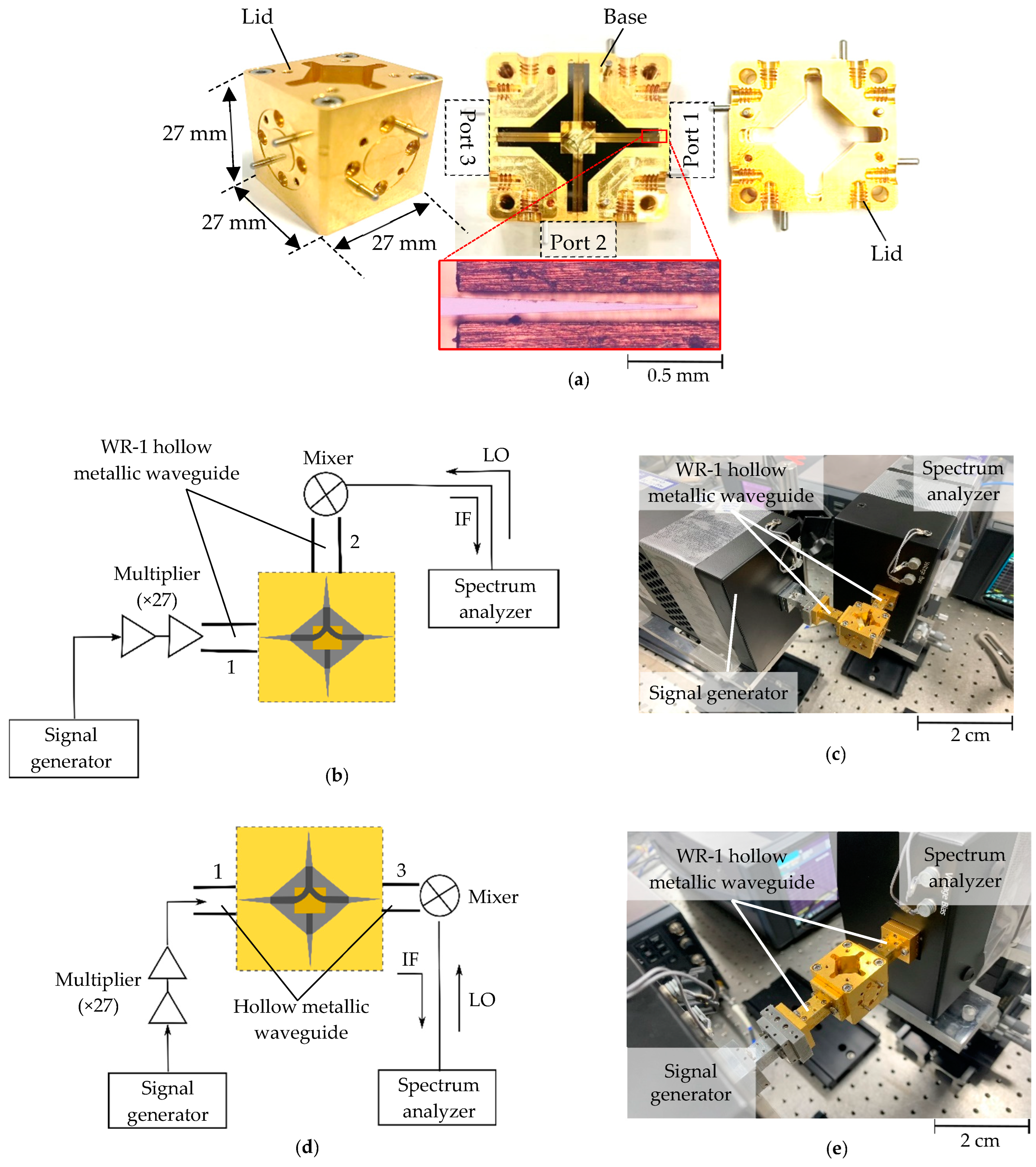
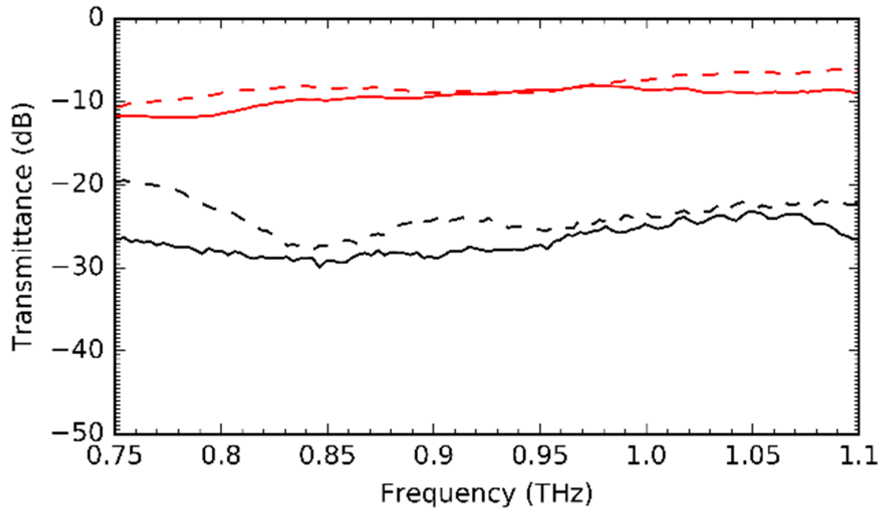
3.3. Y-Junction Module

Having validated the functionality of the developed modules, we developed passive components for the realization of integrated terahertz systems. We implemented a Y-junction, which is an elementary passive component. Y-junctions are versatile components that can serve as both splitters and combiners. The design of the proposed Y-junction is illustrated in Figure 13. This component was implemented with a 2 mm-radius 90°circular bend. The bend was symmetrically reflected to implement the third port of the component. The Y-junction is built on the unclad waveguide described in Section 2. Unclad waveguides are versatile, resemble silicon wires, and can be bent easily with very little loss [23]. However, the implementation of bend structures in EM and photonic crystal platforms has resulted in more losses [29,30]. More recent research has focused on employing VPC to decrease bending losses [2]. The EM section of the Y-junction was similar to that of the unclad waveguide. That is, the lattice is a = 45 μm and the hole diameter is D = 35 μm. For the waveguide core, the Y-branch was implemented with an 80 μm-wide waveguide track instead of 100 μm, as for the unclad waveguide, to increase the clearance between the waveguide track and the walls of the WR-1 standard metallic hollow waveguide module. The inner dimensions of the waveguide were 127 μm × 254 μm. To excite TE modes, the shorter side must be oriented vertically to the unclad waveguide plane. Consequently, having a 100 μm waveguide width leads to a ~20 μm margin left for the insertion of the unclad waveguide into the hollow waveguide via the taper. Therefore, to design the Y-junction, the waveguide track width was chosen to be smaller. Protective frames were also implemented to ensure ease of handling during the experiments and to facilitate integration with metallic packaging. The thickness of the Y-junction was kept the same (80 μm) to allow for fabrication from the same wafer using DRIE.
We fabricated the Y-junction and assembled the Y-junction module with packaging similar to that described in Section 3. The module was 27 mm × 27 mm × 27 mm and was made of copper with gold plating. The assembly was performed in a similar manner, employing tweezers to place the all-Si component onto the base of the packaging, and then the lid was affixed using screws. The assembled module is shown in Figure 14a, with a micrograph of the Si taper within the hollow metallic waveguide. Figure 14a also shows the module ports, following which we probed the transmission power using the setup shown in Figure 6. Figure 14b–e shows the experimental setup for measuring transmittance S21 and isolation S31, respectively. The results of these measurements are shown in Figure 15. Both the simulated (dashed line) and measured (solid line) transmittance and isolation are presented. The measured and simulated transmittances (red) are in good agreement, with very little discrepancy between the lower and upper ends of the entire band of interest. The measured isolation was found to be better than the simulated isolation. Theoretically, the lower the isolation, the better. When isolation is lower, very little power deviates from Port 1 to Port 2, causing most of the power to be transmitted. The isolation in the measurement is found to be approximately −26 dB at 0.75 THz, against −20 dB in simulation.
However, for frequencies >0.85 THz, the simulated and measured isolations are in acceptable agreement, mostly around −25 dB. The discrepancy for the lower frequency is attributed to minor fabricator errors in the unclad section leading to Port 3 of the module. As shown in Figure 4c,d, the unclad waveguide performance is strongly dependent on the waveguide width. A waveguide width of 100 μm has very little loss, with a transmittance of ~−0.3 dB at 0.75 THz. In comparison, a waveguide width of 80 μm has a transmittance of ~1.8 dB at 0.75 THz. This significant difference could affect the overall performance of the Y-junction. Looking at the trends for the transmittance for different values of W, it can be deduced that the transmittance worsens as the waveguide width decreases. As such, a waveguide width W < 80 μm would cause the transmittance to be <−2 dB. Because of the very small dimensions of the Y-junction, fabrication errors occurred, resulting in an increased measured loss at Port 3. In addition, as established through measurements, unclad waveguides have increased loss caused by additional coupling loss at the interface where the EM is interrupted, revealing the waveguide core. For the straight waveguide, two such interfaces exist, accounting for a loss of ~0.4 dB. In case of the Y-junction, there are three such interfaces, which theoretically should account for a total coupling loss of 0.6 dB. Considering the circular bending, these losses could have increased in the fabricated device. This phenomenon stresses the requirement for more accurate machining and is a major hindrance to the currently available techniques.

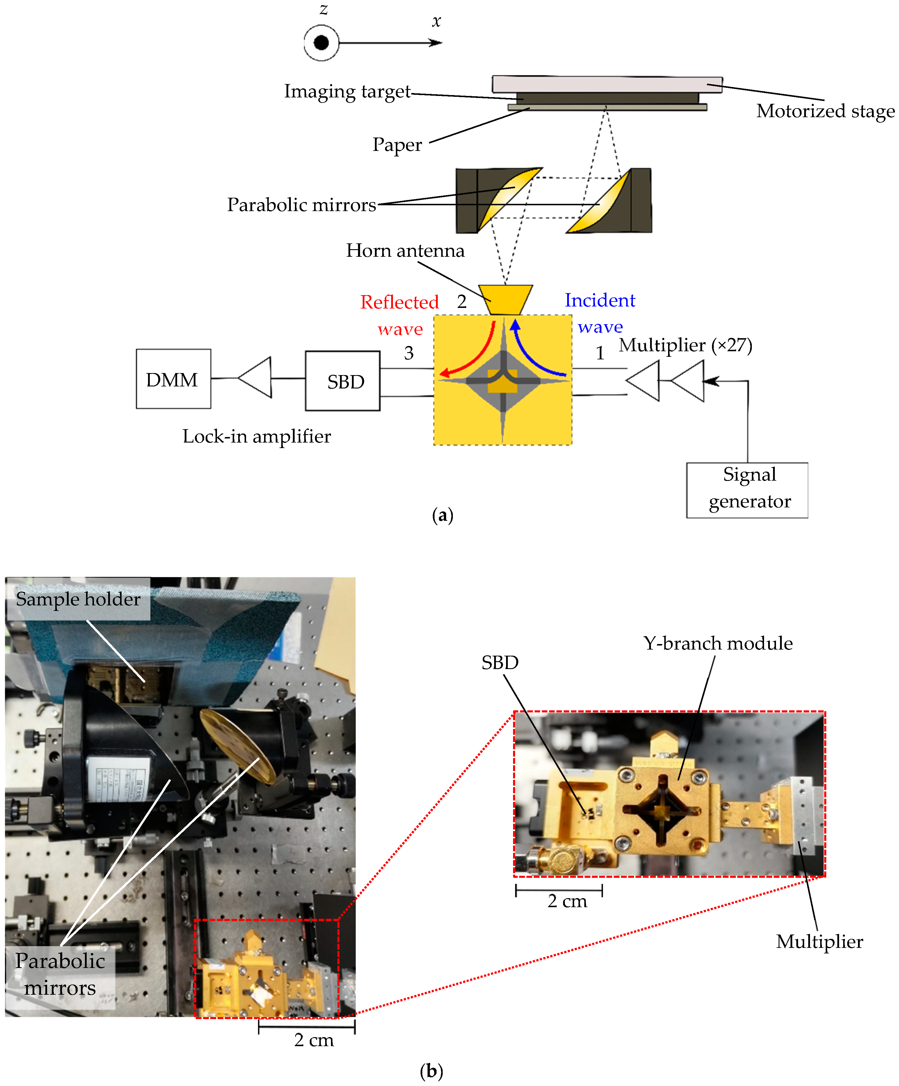
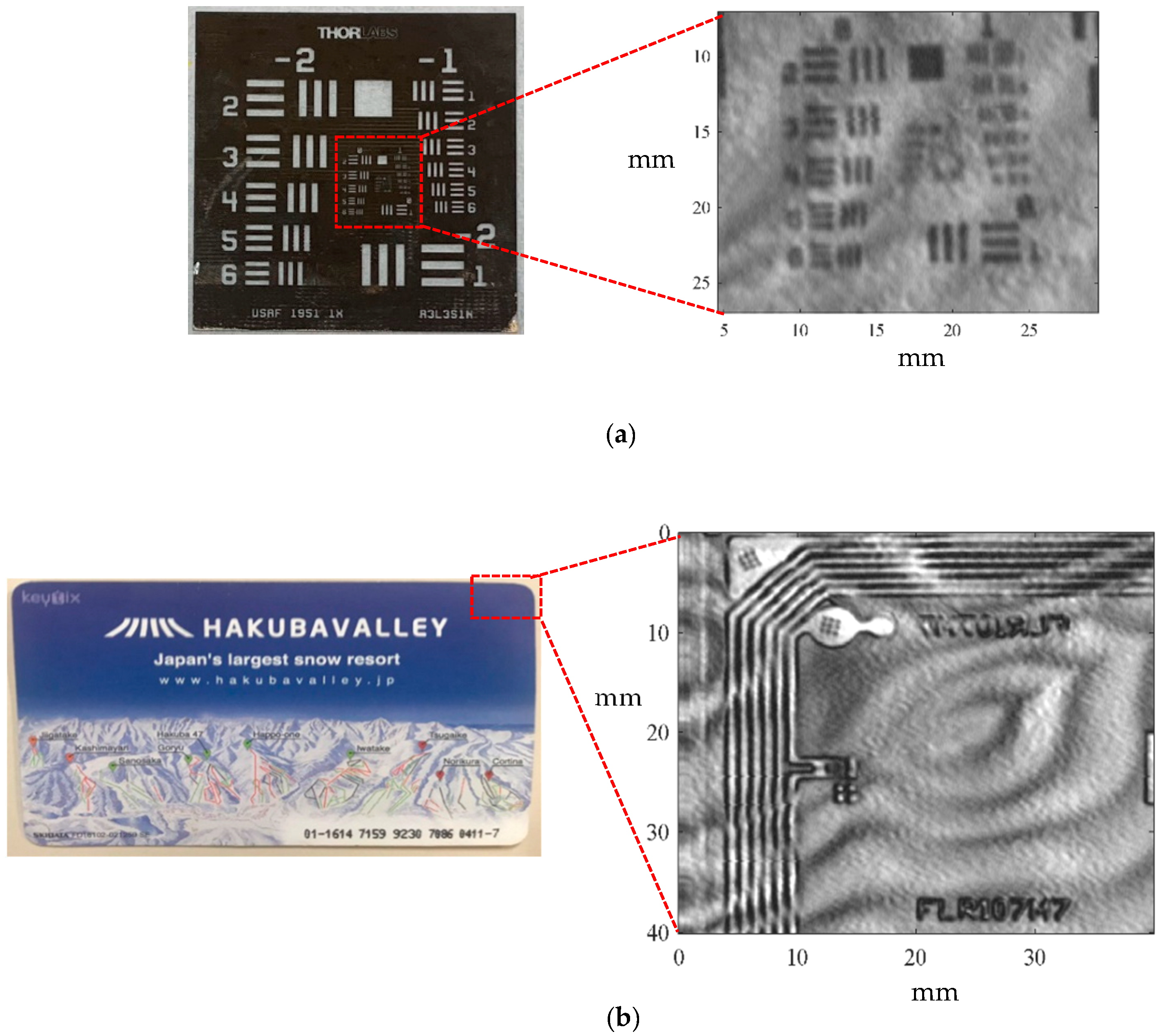
4. Imaging Application

THz waves are well-suited for imaging applications. THz waves can penetrate a wide variety of non-conducting materials such as wood, paper, cardboard, plastic, and ceramic. This has allowed for key novel applications in healthcare for single-strand DNA detection [31] and in security for enhanced non-invasive detection of concealed weapons [7]. Other notable applications have been realized in industrial inspections for the detection of defects [32]. However, imaging applications have been restricted by the physically large size of the systems because of the need for components such as splitters and lenses. Employing a large number of individual components increases the system complexity and imposes a more stringent alignment for optical paths. More practical imaging systems may require a reduction in the physical size and complexity as more compact systems can allow for large-scale hybrid integration and open the door to novel applications. Recent research has sought hybrid integration with flat optics, allowing for the realization of all-Si lenses [33,34], beam splitters [35], and filters [36]. This has significantly reduced the size and complexity of imaging systems, resulting in compact designs that can be handheld [37], enabling applications at higher terahertz frequencies and novel applications such as drone-borne technology.
Having realized and demonstrated the WR-1 band Y-junction module, we attempted to demonstrate the practical imaging applications of this module. Targeting the frequencies in the 0.75–1.1 THz range is a step towards high-resolution imaging applications. To this end, we employed the configuration shown in Figure 16a. At the transmitter side, a ~35.4 GHz millimeter wave signal that is modulated using a 100 kHz signal was injected into a ×27 multiplier to deliver THz waves in the WR-1 band. The terahertz signal was then injected into the Y-junction module through Port 1 and radiated into free space through a horn antenna attached to Port 2. Two parabolic mirrors, one that serves as a collimating mirror and the other as a galvanometer mirror, were employed. The radiated signal from the horn is collimated by the first mirror, which ricochets off the second mirror to reach the target. The target is attached to a motorized stage that allowed both x-axis and z-axis scanning. On the receiver side, the residual signal from the target was detected by a Schottky barrier diode (SBD) and measured by a digital multimeter (DMM) after lock-in detection. Figure 16b shows a photograph of the imaging experimental setup with the Y-junction module as an inset. The imaging results are shown in Figure 17. Figure 17a shows the imaging results for a commercially available test target with paper on top to reproduce a real-life obstacle. The test target was successfully scanned at a resolution of 0.28 mm. Upon successful confirmation of the imaging resolution of the system, imaging of an integrated circuit (IC) card was successful. The results are presented in Figure 17b, revealing that the internal circuit lies beneath the cover of the IC card. The imaging results indicate that THz waves can penetrate nonconducting materials.

5. Conclusions

We have presented WR-1 (0.75–1.1 THz) band dielectric waveguide modules that employ ultra-low-loss and broadband substrateless unclad waveguides and EM waveguides. Experimental validations of these modules revealed superior performance in terms of loss improvement compared to that of standard metallic hollow waveguides. We also developed a Y-branch module that was employed to successfully demonstrate imaging applications at 0.975 THz.
In this study, we have highlighted the process of realizing such waveguide modules to establish a new standard for interconnects in THz systems to replace the long-standing, lossy, hollow waveguide module. The proposed module has the potential of hybrid integration with various dielectric components that are widely employed in the terahertz range. We have demonstrated this in the case of the Y-junction; however, the packaging technique discussed in this study can be extended to interferometers, providing a sturdy, lightweight platform for more sophisticated systems that can be the center of the next generation of applications in the THz range. Building upon the success of hybrid integration between all-Si platforms and active devices such as resonant tunneling diodes and mixer circuits, this technique is not limited to passive components only but also may realize all compact modules of active components.

Author Contributions

Conceptualization, R.K. and M.F.; methodology, R.K. and M.F.; software, R.K.; validation, R.K., R.M., K.I., M.F. and T.N.; formal analysis, R.K. and M.F.; investigation, R.K., R.M. and K.I.; resources, L.Y., M.F. and T.N.; data curation, R.K.; writing—original draft preparation, R.K.; writing—review and editing, L.Y., M.F. and T.N.; visualization, R.K.; supervision, M.F. and T.N.; project administration, M.F. and T.N.; funding acquisition, M.F. All authors have read and agreed to the published version of the manuscript.

Funding

This research was funded by the Core Research for Evolutional Science and Technology (CREST) program of the Japan Science and Technology Agency (JPMJCR21C4), in part by KAKENHI Japan (20H00249), and in part by the National Institute of Information and Communications Technology (NICT), Japan, commissioned research (03001).

Institutional Review Board Statement

Not applicable.

Informed Consent Statement

Not applicable.

Acknowledgments

The authors acknowledge the contributions of Norihiko Shibata for their fruitful discussions. The authors would also like to thank Ryoko Mizuno, Ryohei Kaname and Yosuke Koyabu for their assistance with the experiments.

Conflicts of Interest

The authors declare no conflict of interest.

References

  1. Koala, R.A.S.D.; Fujita, M.; Nagatsuma, T. Nanophotonics-inspired all-silicon waveguide platforms for terahertz integrated systems. Nanophotonics 2022, 11, 1741–1759. [Google Scholar] [CrossRef]
  2. Webber, J.; Yamagami, Y.; Ducournau, G.; Szriftgiser, P.; Iyoda, K.; Fujita, M.; Nagatsuma, T.; Singh, R. Terahertz band communications with topological valley photonic crystal waveguide. J. Light. Technol. 2021, 39, 7609–7620. [Google Scholar] [CrossRef]
  3. Yi, L.; Nishida, Y.; Sagisaka, T.; Kaname, R.; Mizuno, R.; Fujita, M.; Nagatsuma, T. Towards practical terahertz imaging system with compact continuous wave transceiver. J. Light. Technol. 2021, 39, 7850–7861. [Google Scholar] [CrossRef]
  4. Shiode, T.; Mukai, T.; Kawamura, M.; Nagatsuma, T. Giga-bit wireless communication at 300 GHz using resonant tunneling diode detector. In Proceedings of the Asia-Pacific Microwave Conference Proceedings, APMC, Melbourne, VIC, Australia, 5–8 December 2011. [Google Scholar]
  5. Shibata, N.; Uemura, Y.; Kawamoto, Y.; Yi, L.; Fujita, M.; Nagatsuma, T. Silicon dielectric diplexer module for 600-GHz-band frequency-division multiplexing wireless communication. IEEE Trans. Terahertz Sci. Technol. 2022, 12, 334–344. [Google Scholar] [CrossRef]
  6. De Maagt, P.; Bolivar, P.H.; Mann, C. Terahertz science, engineering and systems-from space to earth applications. In Encyclopedia of RF and Microwave Engineering; John Wiley & Sons, Inc.: Hoboken, NJ, USA, 2005; Volume 2, pp. 3–10. [Google Scholar]
  7. Dickinson, J.C.; Goyette, T.M.; Gatesman, A.J.; Joseph, C.S.; Root, Z.G.; Giles, R.H.; Waldman, J.; Nixon, W.E. Terahertz imaging of subjects with concealed weapons. Terahertz Mil. Secur. Appl. IV 2006, 6212, 62120Q. [Google Scholar] [CrossRef] [Green Version]
  8. Siegel, P. Terahertz technology in biology and medicine. IEEE Trans. Microw. Theory Tech. 2004, 52, 2438–2447. [Google Scholar] [CrossRef]
  9. Okamoto, K.; Tsuruda, K.; Diebold, S.; Hisatake, S.; Fujita, M.; Nagatsuma, T. Terahertz sensor using photonic crystal cavity and resonant tunneling diodes. J. Infrared Millim. Terahertz Waves 2017, 38, 1085–1097. [Google Scholar] [CrossRef]
  10. Tsuruda, K.; Okamoto, K.; Diebold, S.; Hisatake, S.; Fujita, M.; Nagatsuma, T. Terahertz sensing based on photonic crystal cavity and resonant tunneling diode. In Proceedings of the 2016 Progress in Electromagnetic Research Symposium (PIERS), Shanghai, China, 8–11 August 2016; pp. 3922–3926. [Google Scholar] [CrossRef]
  11. Diebold, S.; Nishio, K.; Nishida, Y.; Kim, J.; Tsuruda, K.; Mukai, T.; Fujita, M.; Nagatsuma, T. High-speed error-free wireless data transmission using a terahertz resonant tunnelling diode transmitter and receiver. Electron. Lett. 2016, 52, 1999–2001. [Google Scholar] [CrossRef]
  12. Song, H.J.; Nagatsuma, T. Handbook of Terahertz Technologies: Devices and Applications, 1st ed.; Pan Stanford: Singapore, 2015. [Google Scholar]
  13. Yang, S.-H.; Jarrahi, M. Navigating terahertz spectrum via photomixing. Opt. Photonics News 2020, 31, 36–43. [Google Scholar] [CrossRef]
  14. Schroder, D.; Thomas, R.; Swartz, J. Free carrier absorption in silicon. IEEE J. Solid-State Circuits 1978, 13, 180–187. [Google Scholar] [CrossRef]
  15. Williams, G.P. Filling the THz gap—High power sources and applications. Rep. Prog. Phys. 2005, 69, 301–326. [Google Scholar] [CrossRef]
  16. Yu, X.; Sugeta, M.; Yamagami, Y.; Fujita, M.; Nagatsuma, T. Simultaneous low-loss and low-dispersion in a photonic-crystal waveguide for terahertz communications. Appl. Phys. Express 2019, 12, 012005. [Google Scholar] [CrossRef]
  17. Tsuruda, K.; Fujita, M.; Nagatsuma, T. Extremely low-loss terahertz waveguide based on silicon photonic-crystal slab. Opt. Express 2015, 23, 31977–31990. [Google Scholar] [CrossRef]
  18. Withayachumnankul, W.; Fujita, M.; Nagatsuma, T. Integrated silicon photonic crystals toward terahertz communications. Adv. Opt. Mater. 2018, 6, 1800401. [Google Scholar] [CrossRef] [Green Version]
  19. TorresGarcia, A.E.; Escudero, J.M.M.P.; Teniente, J.; Gonzalo, R.; Ederra, I. Silicon integrated subharmonic mixer on a photonic-crystal platform. IEEE Trans. Terahertz Sci. Technol. 2021, 11, 79–89. [Google Scholar] [CrossRef]
  20. Koala, R.; Headland, D.; Yu, X.; Nishida, Y.; Fujita, M.; Nagatsuma, T. Terahertz RTD chip backside-coupled to photonic-crystal waveguide. In Proceedings of the 2021 46th International Conference on Infrared, Millimeter and Terahertz Waves (IRMMW-THz), Chengdu, China, 29 August–3 September 2021; Volume 2021, pp. 1–2. [Google Scholar] [CrossRef]
  21. Yu, X.; Hosoda, Y.; Miyamoto, T.; Obata, K.; Kim, J.; Fujita, M.; Nagatsuma, T. Terahertz fibre transmission link using resonant tunnelling diodes integrated with photonic-crystal waveguides. Electron. Lett. 2019, 55, 398–400. [Google Scholar] [CrossRef]
  22. Gao, W.; Yu, X.; Fujita, M.; Nagatsuma, T.; Fumeaux, C.; Withayachumnankul, W.; Xiongbin, Y. Effective-medium-cladded dielectric waveguides for terahertz waves. Opt. Express 2019, 27, 38721–38734. [Google Scholar] [CrossRef] [PubMed] [Green Version]
  23. Headland, D.; Withayachumnankul, W.; Yu, X.; Fujita, M.; Nagatsuma, T. Unclad microphotonics for terahertz waveguides and systems. J. Light. Technol. 2020, 38, 6853–6862. [Google Scholar] [CrossRef]
  24. Subashiev, A.; Luryi, S. Modal control in semiconductor optical waveguides with uniaxially patterned layers. J. Light. Technol. 2006, 24, 1513–1522. [Google Scholar] [CrossRef] [Green Version]
  25. Kawamoto, Y.; Shibata, N.; Uemura, Y.; Iwamatsu, S.; Nishida, Y.; Fujita, M.; Nagatsuma, T. Integrated resonant tunneling diode with rectangular wave guide I/O using photonic crystal interface. In Proceedings of the 2021 46th International Conference on Infrared, Millimeter and Terahertz Waves (IRMMW-THz), Chengdu, China, 29 August–3 September 2021; Volume 2021, pp. 1–2. [Google Scholar] [CrossRef]
  26. Shibata, N.; Uemura, Y.; Kawamoto, Y.; Yi, L.; Fujita, M.; Nagatsuma, T. 600-GHz-band silicon dielectric waveguide module. In Proceedings of the 2021 46th International Conference on Infrared, Millimeter and Terahertz Waves (IRMMW-THz), Chengdu, China, 29 August–3 September 2021; Volume 2021, pp. 1–2. [Google Scholar] [CrossRef]
  27. Headland, D.; Fujita, M.; Nagatsuma, T. Bragg-mirror suppression for enhanced bandwidth in terahertz photonic crystal waveguides. IEEE J. Sel. Top. Quantum Electron. 2020, 26, 4900109. [Google Scholar] [CrossRef]
  28. Koala, R.A.S.D.; Headland, D.; Yamagami, Y.; Masayuki, F.; Nagatsuma, T. Broadband terahertz dielectric rod antenna array with integrated half-Maxwell fisheye lens. In Proceedings of the 2020 International Topical Meeting on Microwave Photonics (MWP), Matsue, Japan, 24–26 November 2020; pp. 54–57. [Google Scholar] [CrossRef]
  29. Chutinan, A.; Noda, S. Waveguides and waveguide bends in two-dimensional photonic crystal slabs. Phys. Rev. B 2000, 62, 4488–4492. [Google Scholar] [CrossRef]
  30. Johnson, S.G.; Villeneuve, P.R.; Fan, S.; Joannopoulos, J.D. Linear waveguides in photonic-crystal slabs. Phys. Rev. B 2000, 62, 8212–8222. [Google Scholar] [CrossRef] [Green Version]
  31. Toccafondo, V.; García-Rupérez, J.; Bañuls, M.-J.; Griol, A.; Castelló, J.G.; Peransi-Llopis, S.; Maquieira, A. Single-strand DNA detection using a planar photonic-crystal-waveguide-based sensor. Opt. Lett. 2010, 35, 3673–3675. [Google Scholar] [CrossRef] [PubMed]
  32. Quast, H.; Loffler, T. 3D-terahertz-tomography for material inspection and security. In Proceedings of the 2009 34th International Conference on Infrared, Millimeter, and Terahertz Waves, Busan, Korea, 21–25 September 2009; pp. 1–2. [Google Scholar] [CrossRef]
  33. Withayachumnankul, W.; Yamada, R.; Fujita, M.; Nagatsuma, T. All-dielectric rod antenna array for terahertz communications. APL Photonics 2018, 3, 051707. [Google Scholar] [CrossRef] [Green Version]
  34. Headland, D.; Klein, A.K.; Fujita, M.; Nagatsuma, T. Dielectric slot-coupled half-Maxwell fisheye lens as octave-bandwidth beam expander for terahertz-range applications. APL Photonics 2021, 6, 096104. [Google Scholar] [CrossRef]
  35. Lee, W.S.L.; Nirantar, S.; Headland, D.; Bhaskaran, M.; Sriram, S.; Fumeaux, C.; Withayachumnankul, W. Broadband terahertz circular-polarization beam splitter. Adv. Opt. Mater. 2018, 6, 1700852. [Google Scholar] [CrossRef]
  36. Gao, W.; Lee, W.S.L.; Fumeaux, C.; Withayachumnankul, W. Effective-medium-clad Bragg grating filters. APL Photonics 2021, 6, 076105. [Google Scholar] [CrossRef]
  37. Sagisaka, T.; Kaname, R.; Kikuchi, M.; Kukutsu, N.; Headland, D.; Yi, L.; Fujita, M.; Nagatsuma, T. Integrated terahertz optics with effective medium for 600-GHz-band imaging. In Proceedings of the 2020 International Topical Meeting on Microwave Photonics (MWP), Matsue, Japan, 24–26 November 2020. [Google Scholar] [CrossRef]
Figure 1. Designs of proposed dielectric waveguides: (a) Unclad waveguide; (b) EM waveguide; W = 100 μm, D = 35 μm, a = 45 μm and T = 80 μm.
Photonics 09 00515 g001
Figure 2. Electric field distribution at 0.925 THz: (a) Unclad waveguide; (b) EM waveguide.
Photonics 09 00515 g002
Figure 3. Refractive index of the EM section as a function of the hole diameter.
Photonics 09 00515 g003
Figure 4. Analysis of the impact of T and W on the performance of 1 cm-long unclad waveguide and EM waveguide: (a) Transmittance of unclad waveguide for T = 70 μm (green), T = 80 μm (black), T = 90 μm (red) and W is fixed at 100 μm; (b) Transmittance of EM waveguide for variable T with fixed W = 100 μm; (c) Transmittance of unclad waveguide for W = 80 μm (red), W = 90 μm (green), W = 100 μm (black) and T is fixed at 80 μm; (d) Transmittance of EM waveguide for variable W with fixed T = 80 μm.
Photonics 09 00515 g004
Figure 5. Fabricated waveguide samples with micrographs as inset: (a) Unclad waveguides; (b) EM waveguides.
Photonics 09 00515 g005
Figure 6. Experimental setup for the measurement of the transmittance: (a) Schematic of the setup; (b) Photograph of the setup.
Photonics 09 00515 g006
Figure 7. Measured transmittance of the fabricated waveguides: (a) 1 cm unclad waveguide; (b) 1 cm EM waveguide; (c) 2 cm unclad waveguide; (d) 2 cm EM waveguide; (e) 3 cm unclad waveguide; (f) 3 cm EM waveguide; (g) 4 cm unclad waveguide; (h) 4 cm EM waveguide; (i) 5 cm unclad waveguide; (j) 5 cm EM waveguide.
Photonics 09 00515 g007
Figure 8. Measured total loss at 0.925 THz as a function of waveguide length: (a) Total loss of unclad waveguide; (b) Total loss of EM waveguide. The propagation loss is defined using the slope. The coupling loss is defined using the intercept.
Photonics 09 00515 g008
Figure 9. Measured (solid) and simulated (dashed) propagation loss and coupling loss: (a) Propagation loss of unclad waveguides; (b) Propagation loss of EM waveguide; (c) Coupling loss of unclad waveguide; (d) Coupling loss of EM waveguide.
Photonics 09 00515 g009
Figure 10. Concept of the proposed module, highlighting the transition and connection interfaces.
Photonics 09 00515 g010
Figure 11. Fabricated modules and experimental setup: (a) Unclad waveguide module; (b) EM waveguide module; (c) Hollow metallic waveguide; (d) Experimental setup.
Photonics 09 00515 g011
Figure 12. Measured (solid) and simulated (dashed) transmittance of fabricated modules. The modules are 56.2 mm-long. The unclad and EM modules incorporate each 50 mm unclad and 50 mm EM waveguide, respectively.
Photonics 09 00515 g012
Figure 13. Design of proposed Y-branch with the effective medium section as inset. W = 80 μm, T = 80 μm, D = 45 μm, P = 45 μm.
Photonics 09 00515 g013
Figure 14. Y-branch measurement setup: (a) Fabricated module; (b) Block diagram for the measurement of S21; (c) Photograph of experiments setup for the measurement of S21; (d) Diagram for the measurement of S31; (e) Photograph of the experimental set up for the measurement of S31.
Photonics 09 00515 g014
Figure 15. Measured S21 (red) and S31 (black) of proposed Y-branch (dashed lines) and Y-branch module (solid lines).
Photonics 09 00515 g015
Figure 16. Imaging experimental setup: (a) Block diagram of the setup; (b) Photograph of the measurement showing the Y-branch module as inset.
Photonics 09 00515 g016
Figure 17. Imaging results at 0.957 THz: (a) Imaging of test target without paper; (b); (b) Imaging results of an IC card.
Photonics 09 00515 g017
Publisher’s Note: MDPI stays neutral with regard to jurisdictional claims in published maps and institutional affiliations.

