1. Introduction
Optical frequency comb (OFC) has wide application prospects in many fields, such as optical arbitrary waveform generation [
1], ultra-large capacity optical communication system [
2], precise measurement and sensing [
3,
4], and photonic microwave signal processing [
5], etc. In the current research literature, there are mainly the following methods for generating optical frequency comb: mode-locked laser method [
6,
7,
8], micro-ring resonator method [
9], fiber nonlinear effect method [
10,
11], external modulator method [
12,
13,
14,
15], gain-switching (GS) laser technique [
16,
17,
18] and the recirculating frequency shift (RFS) method [
19,
20,
21,
22,
23,
24,
25,
26,
27,
28]. Each of the above methods has its own advantages and disadvantages. The mode-locked laser method can generate broadband optical frequency combs, but the tunability of the frequency spacing and the flatness of the comb lines are poor. The micro-ring resonator method has an integrated structure and can generate optical frequency combs with a lot of comb lines, but the design is complex, and the spectral interval is difficult to adjust. The fiber nonlinear effect method can generate the optical frequency combs with a wide spectral bandwidth, but the flatness of the generated optical frequency combs is poor. The external modulator method can generate optical frequency combs with good flatness and tunability, but the number of comb lines is limited. The gain-switching laser technique is highly tunable and can generate high-quality comb lines, but its total bandwidth is small compared with some other methods, and increasing the bandwidth will increase the overall cost and complexity.
The RFS method has attracted much attention because the method can generate optical frequency combs with a large number of comb lines and good flatness, there are experimental reports that the number of generated comb lines is up to hundreds, and the flatness is less than 5 dB, but the noise will continue to accumulate with the number of cycles, resulting in the reduction of optical signal-to-noise ratio (OSNR) of the comb lines. The RFS method is generally based on the electro-optical modulation technique to obtain carrier suppressed single sideband (SSB) signal for recirculating frequency shift in the RFS loop. The RFS method is mainly divided into two ways: one is unidirectional circulation in a single loop [
20,
21,
22,
23,
24,
25], and the other is circulation in two directions in a double-loop [
26,
27,
28]. When the number of cycles is the same, the number of comb lines generated by the method of double-loop bidirectional recirculation frequency shift is twice that of the single-loop method. Since the noise accumulation of the generated optical frequency comb is related to the number of cycles, the method of double-loop bidirectional recirculation frequency shift has less noise accumulation; thus, it can generate flatter optical frequency combs with a better signal-to-noise ratio, but the complex structure of the double-loop system is one of its shortcomings. The Ref. [
19] proposed a scheme of bidirectional recirculating frequency shift in single loop for generating flat and broadband optical frequency combs, but the influence of the carrier on the generated OFCs cannot be ignored when the extinction ratio of the modulator is not high.
In this paper, we propose a new scheme of optical frequency comb generation system based on single-loop bidirectional recirculation frequency shifting, which can realize simultaneous circulation in two directions in one loop; that is to say, the frequency shifting of newly generated comb lines has two trends, one is frequency increasing, another is frequency decreasing. The scheme uses two pairs of dual-drive Mach–Zehnder modulators and several polarization devices. Compared with the method of using single-loop unidirectional recirculation frequency shifting, when generating the same number of comb lines, the number of cycles is halved, the noise accumulation becomes less, and better flatness is achieved. Compared with the double-loop recirculation frequency shifting scheme, the proposed optical frequency comb generation system is simpler in structure. Compared with Ref. [
19], the proposed scheme can further reduce the adverse effect of carriers on the generation of optical frequency combs.
2. The Principle of the Ultra-Flat OFC Generation Scheme
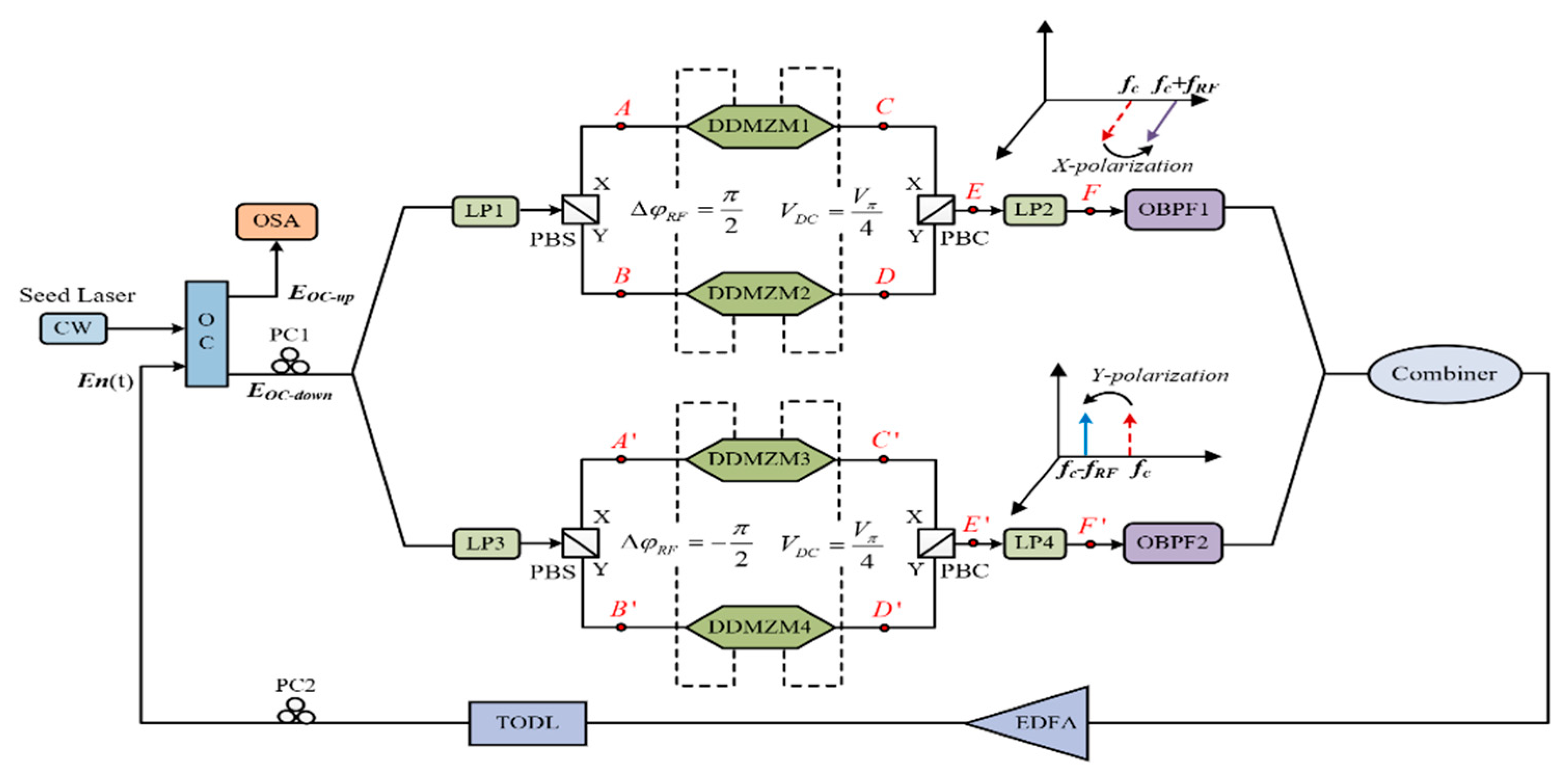
The basic structure of the proposed OFC generation system is shown in
Figure 1. The system structure mainly includes the following devices: continuous-wave laser (CW Laser), polarization controller (PC), linear polarizer (LP), polarization beam splitter (PBS), dual-drive Mach–Zehnder modulator (DDMZM), polarization beam combiner (PBC), adjustable optical band-pass filter (OBPF), erbium-doped fiber amplifier (EDFA), tunable optical delay line (TODL), and optical coupler (OC). The output OFC of the system is observed by an optical signal analyzer (OSA).
The seed optical signal generated by the CW Laser is imported into the loop through the OC, then it is equally divided into two branches; in each branch, the optical signal is divided into two orthogonal polarization signals by the PBS and separately modulated by a pair of DDMZMs, then via PBC, LP, and OBPF, only +1st-order or −1st-order modulated optical signal with one given polarization state is outputted in the branch. By reasonable setting, one branch can generate +1st-order modulated optical signal, the other branch can generate −1st-order modulated optical signal, and the polarization of the optical signals from the two branches is orthogonal. Then, the two modulated optical signals are combined, power amplified, and delay adjusted; finally, they are coupled with the seed laser by the OC. One output port of the OC connects with OSA to show the generated OFC, and the two modulated optical signals are injected into the loop for recirculation via another output port of the OC. The frequencies of the modulated optical signals shift to both sides of the center frequency (i.e., the frequency of seed laser). Two new spectral lines can be generated per cycle.
Assume that the signal of the seed laser is
,
is the amplitude of the optical signal, and
denotes its angular frequency. The transfer function of the OC in
Figure 1 can be expressed as:
Then, the output signal of the OC for the first circulation in the loop is
. Here, we firstly consider the situation of the upper branch. For the convenience of description, assuming that the input signal of the PBS is
, where
. Set the angle of LP1 to
; then, the output of the PBS at A and B points can be expressed as:
A single DDMZM is firstly analyzed by setting the modulator in push-pull mode. The DC bias voltage on each arm of the modulator is
, and the phase change caused by DC bias on each arm of the modulator is
, where
is the half-wave voltage of the modulator. The amplitude and angular frequency of the RF drive signal on the upper and lower arms of the DDMZM are
and
, respectively. The RF drive signals loaded on the upper and lower arm can be represented as
and
, where
and
are the initial phases of the two RF drive signals, so the initial phase difference is
. The modulated output signal of the DDMZM can be expressed as:
where
,
m is the modulation index of the RF signals. The right side of Equation (3) can be expanded into the Bessel function, when
m is small and
, the output signals of port
C and port
D can be expressed as:
where
represents the first-order Bessel function, and
is the order of sideband harmonics of the modulated optical signals. The signals of the port
C and port
D are input to the PBC. By setting the angle of PBC to
, then the optical signal at the E point can be expressed as:
By analyzing Equation (5), we can find that only the 1st-order sideband signal exists on the X-polarization, and the seed laser signal and quadrature component of the 1st-order sideband signal exist on the Y-polarization. Here, the X-polarization and the Y-polarization are orthogonal. By adjusting the rotation angle of linear polarizer LP2, then the signal of Y-polarization is removed, and interference of the seed laser to the SSB signal is eliminated, so the purer 1st-order SSB signal with the X-polarization can be obtained.
Similarly, we can analyze the situation of the lower branch, and finally, the optical signal at the
point can be expressed as:
From Equation (6), we can find that only the −1st-order sideband signal exists on the Y-polarization. By adjusting the rotation angle of linear polarizer LP4, then the pure −1st-order sideband signal with the Y-polarization can be obtained, and the signal of X-polarization is removed.
Finally, the optical signal at point
F and point
can be expressed as:
From Equation (7), we can see that via the upper branch, the frequency of the seed laser is shifted to a positive direction with the frequency shift of , and via the lower branch, the frequency of the seed laser is shifted to a negative direction with the frequency shift of . The polarization of the output signal of the upper branch and that of the lower branch is orthogonal.
The two polarization signals are filtered by corresponding OBPF and combined into one signal by an optical combiner, then the combined signal is amplified by EDFA for power compensation to eliminate the influence of transmission loss, and the TODL is used to compensate for the effect of delay; finally, the combined signal and the seed laser are coupled by the OC, and the first cycle is completed. After the first cycle, the optical signal with the angular frequency of and can be generated; that is to say, two new spectral lines are added to the spectrum of the output signal of the OC. In fact, in subsequent cycles, each cycle will add two new spectral lines.
The optical signal completing the first cycle in the loop at the input port of the OC can be expressed as [
19]:
where
G is the gain of the EDFA,
L represents the total loss of one cycle in the loop, and
τ denotes the delay per cycle.
h(
t) represents the response of OBPF in time domain, assuming that its frequency domain transfer function is a rectangular function, and the following conditions need to be satisfied:
M is the final number of output comb lines of the OFC generation system. Let
N is the number of cycles for generating
M-line OFC, then
M = 2
N + 1. The output optical signal of the system after
N cycles can be expressed as:
where
is the optical signal in the loop at the input port of the OC after
N cycles. From the above equation, the angular frequency components of the output optical signal of the system can be expressed as
, these frequency components constitute an optical frequency comb in the frequency domain. The frequency interval of the generated optical frequency comb is only determined by the angular frequency of the RF signal and can be adjusted.
In the loop, the delay
can affect the quality of the generated optical frequency comb, an inappropriate delay will cause phase noise of the comb lines, and the phase noise can be converted into intensity noise of the generated optical combs, thus causing power fluctuation of the comb lines. On the other hand, the delay in the loop may influence the orthogonality of the comb lines. TODL can adjust the delay in the loop when the two equations
and
are simultaneously satisfied, a better optical frequency comb can be generated. Under this condition, Equation (10) can be simplified as:
3. Numerical Simulation and Results Discussion
In order to verify the feasibility of the proposed scheme, in this section, we use the VPI TransmissionMaker software to simulate the optical frequency comb generation system. The simulation is based on the schematic shown in
Figure 1.
In the simulation, the output power, center frequency, and linewidth of the seed laser are 0 dBm, 193.1 THz, and 1 MHz, respectively. All the DDMZMs are in push–pull mode, and the half-wave voltage , the extinction ratio is set to 30 dB. The range of noise figure for an amplifier is generally 4~6 dB; in this simulation, the noise figure is set to 4 dB. Flatness is defined as the maximum power difference between the comb lines.
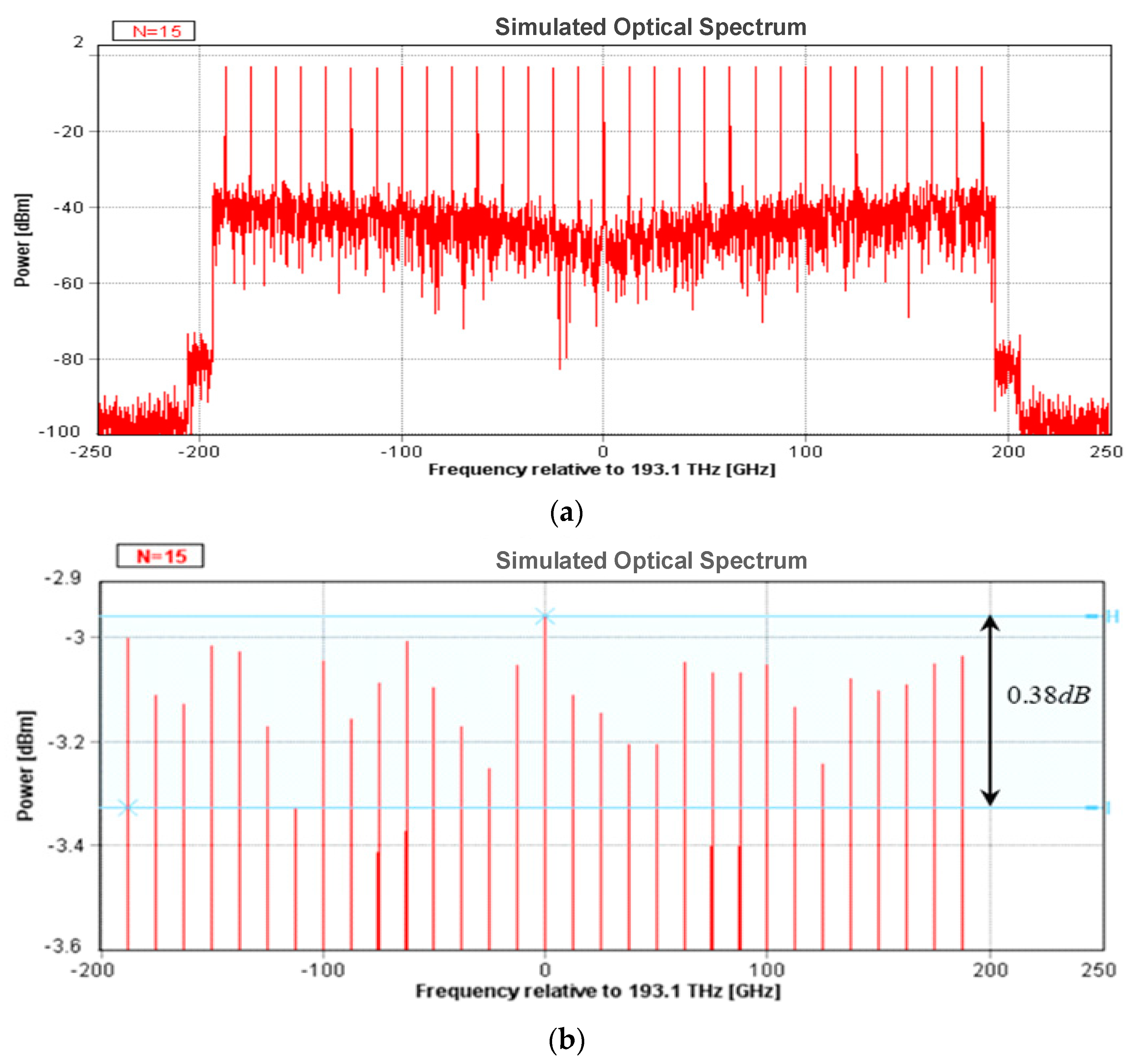
Figure 2a shows the spectrum of a 31-line optical frequency comb with the line spacing of 12.5 GHz and the flatness of about 0.38 dB after cycling 15 times. For the convenience of measuring the flatness of the optical frequency comb, the top of the optical frequency comb is enlarged, as shown in
Figure 2b. In Ref. [
19], the flatness of 31-line OFC is 0.86 dB, and the flatness is improved by about 0.48 dB by the method proposed in this paper.
According to the analysis in
Section 2, in order to obtain a flat optical comb, the delay
should satisfy the two functions
and
at the same time. The parameter
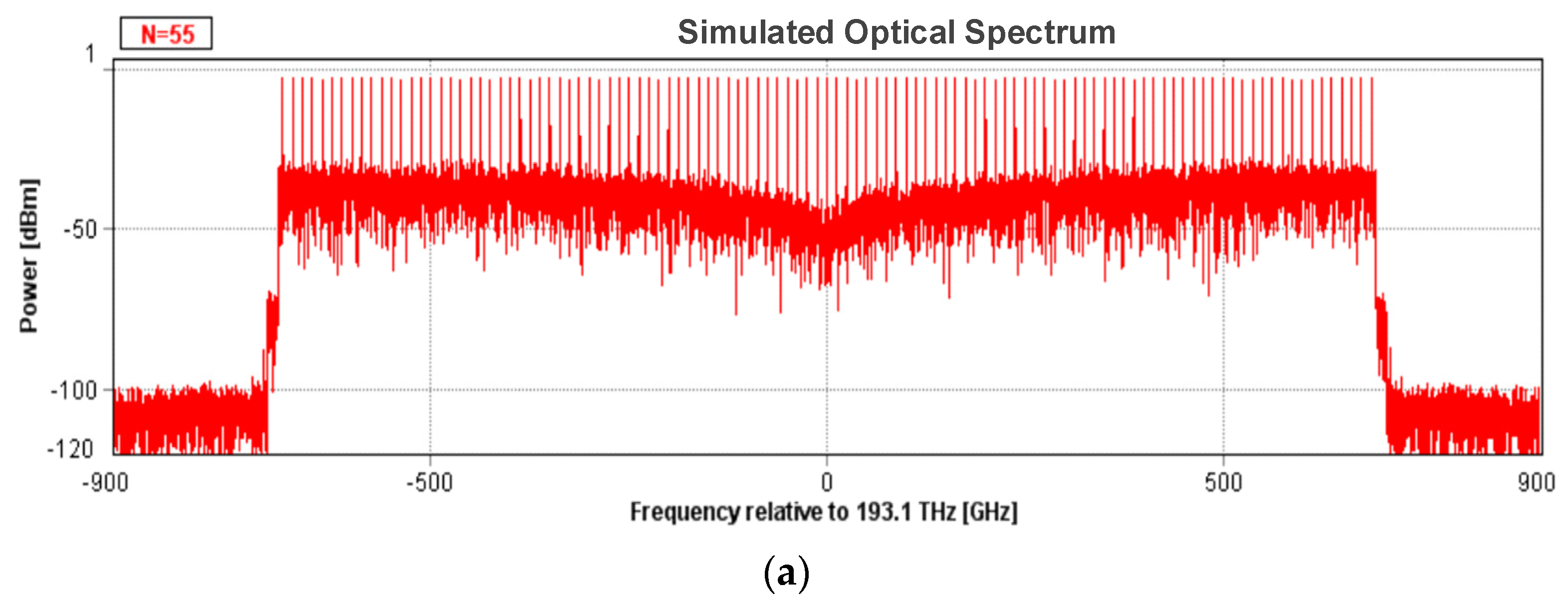
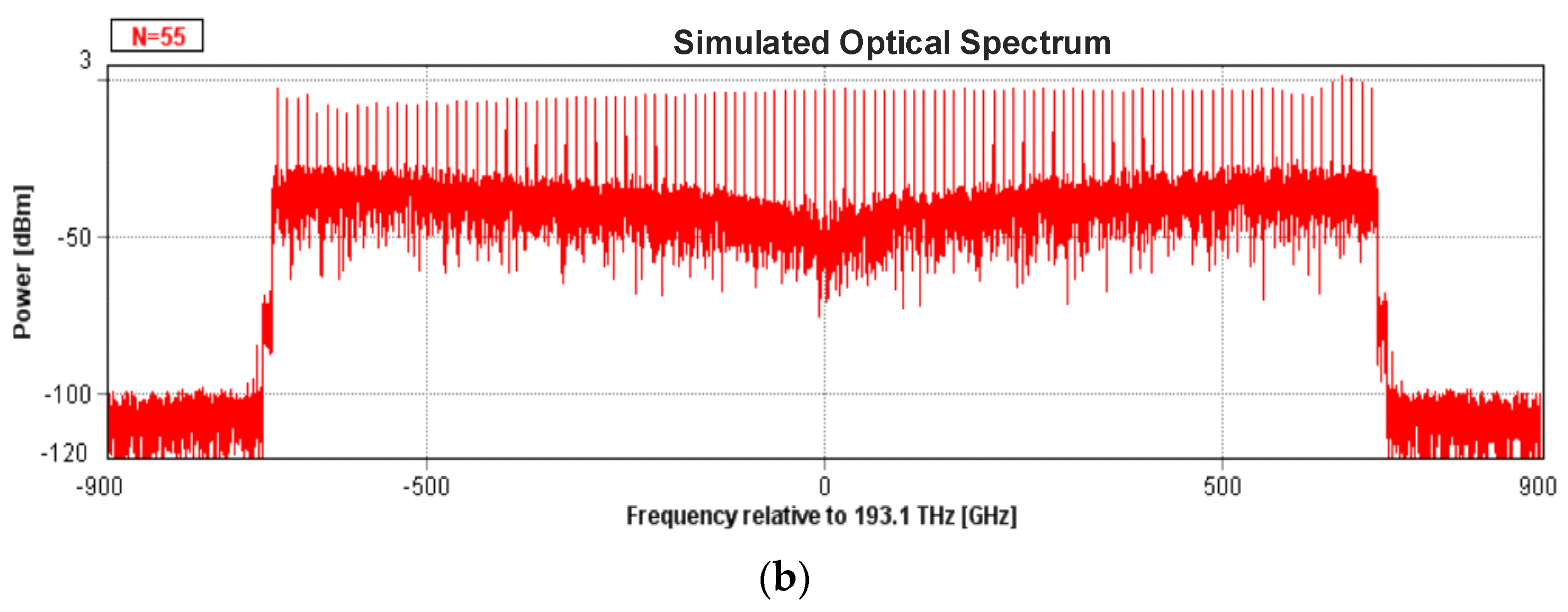
can be adjusted by TODL. Here, the effect of the TODL on the generation of optical frequency combs is studied. Assume the seed laser is cycled 55 times, then a 111-line optical frequency comb with
line spacing will be generated.
Figure 3a shows the generated optical frequency comb when TODL is used in the loop and is appropriately adjusted.
Figure 3b shows the generated 111-line optical frequency comb without the TODL in the loop.
In this case, the flatness of the optical frequency comb is measured. The flatness in
Figure 3a is 0.76 dB, while the flatness in
Figure 3b is 11.08 dB. The flatness difference is 10.32 dB, which indicates that the use of TODL in the loop can improve the flatness of the optical comb, and TODL plays an important role in the scheme. The following studies are based on the use of TODL in the loop.
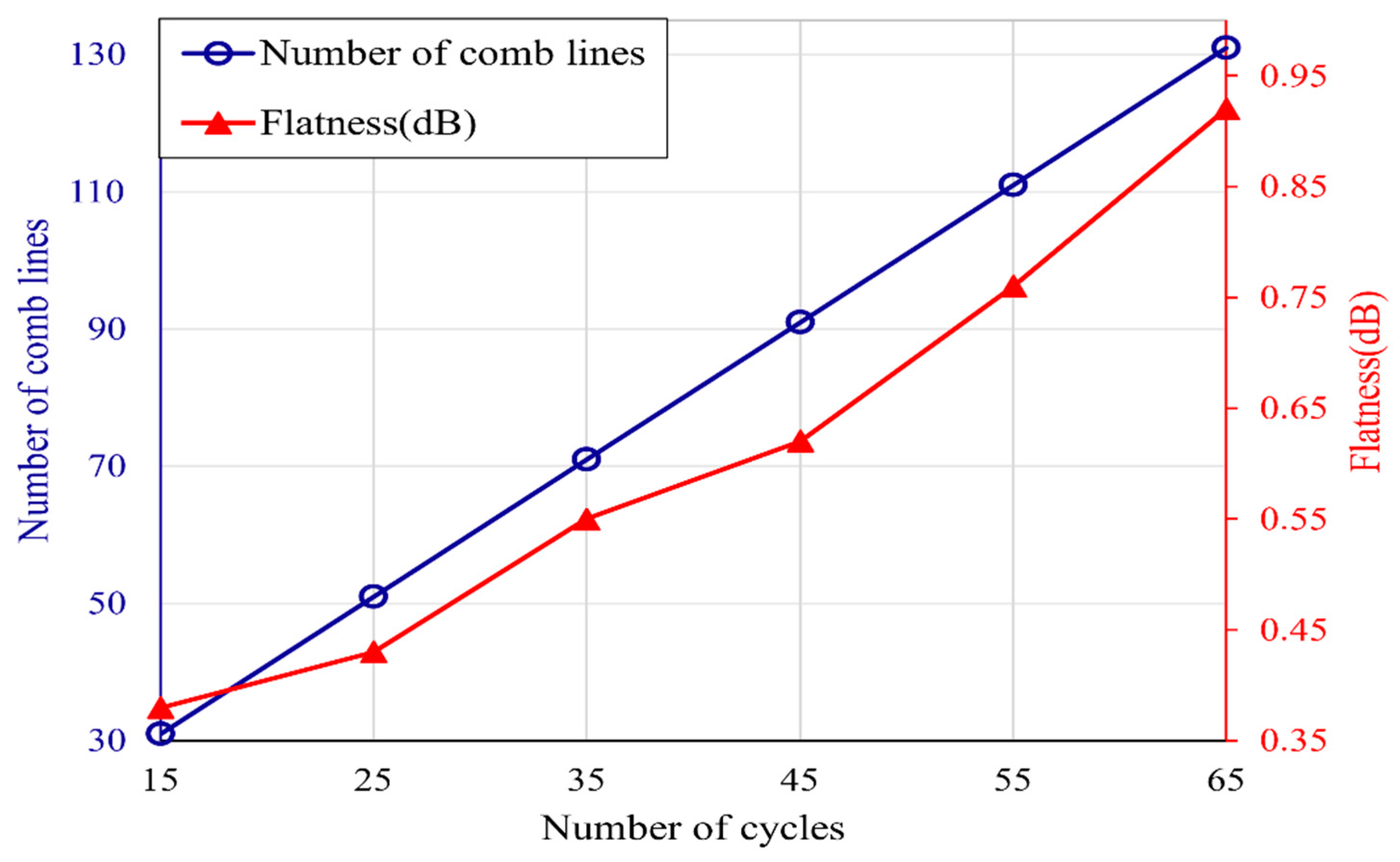
The number of comb lines is determined by the number of cycles of the seed laser in the loop; here, its effect on the flatness of comb lines is investigated by varying the number of cycles.
Figure 4 shows the flatness and the number of comb lines under different numbers of cycles. It can be seen that when the number of cycles increases, the number of comb lines increases in proportion, and the flatness becomes poor, that is because the accumulation of ASE noise of the amplifier in the loop. The more cycles in the loop, the more lines of the generated optical frequency comb, but the worse of the flatness.
Table 1 shows the comparison of flatness of the generated OFCs with Ref. [
19] for different numbers of comb lines. It can be seen that when the generated OFCs have the same number of comb lines, the OFC flatness of the proposed scheme will be better than that of Ref. [
19]. That is because the adverse influence of carrier on the generation of optical frequency combs cannot be ignored when the extinction ratio of the modulator is not high; however, the proposed scheme can eliminate the effect of carrier on the generated OFCs by adjusting the rotation angle of linear polarizer, the purer SSB signal can be obtained, and the flatness of comb lines is improved.
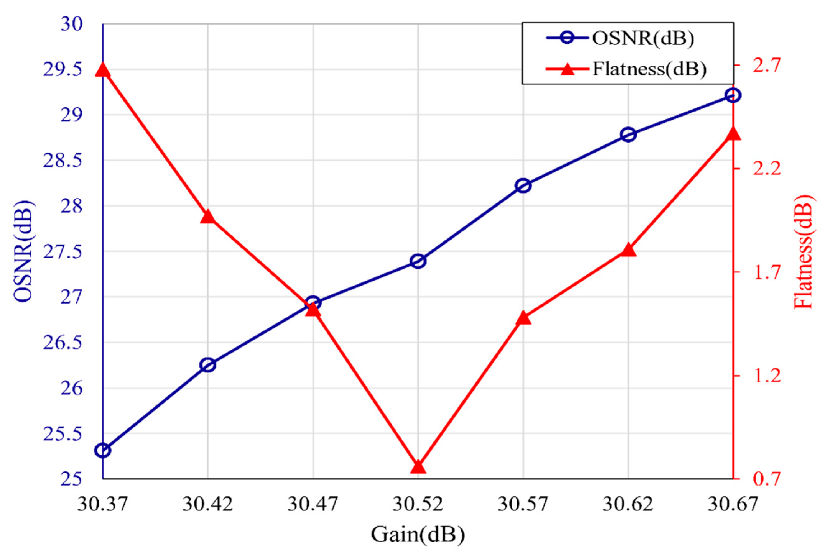
From the theory analysis in
Section 2, EDFA is used to compensate for the power loss of the seed laser in the loop; EDFA gain will influence the generated optical frequency comb.
Figure 5 shows the flatness and optical signal-to-noise ratio (OSNR) of the 111-line optical frequency comb under different EDFA gains. It can be seen that the flatness varies with the gain values, and there is an optimal gain of 30.52 dB at which the flatness is the best; the best flatness is 0.76 dB when the EDFA gain value is set less than or greater than the optimal gain, the flatness will become worse, for example, the flatness is greater than 2 dB when the gain is set to 30.37 dB and 30.67 dB. At the same time,
Figure 5 shows that the OSNR of the comb line is increasing with the EDFA gain.
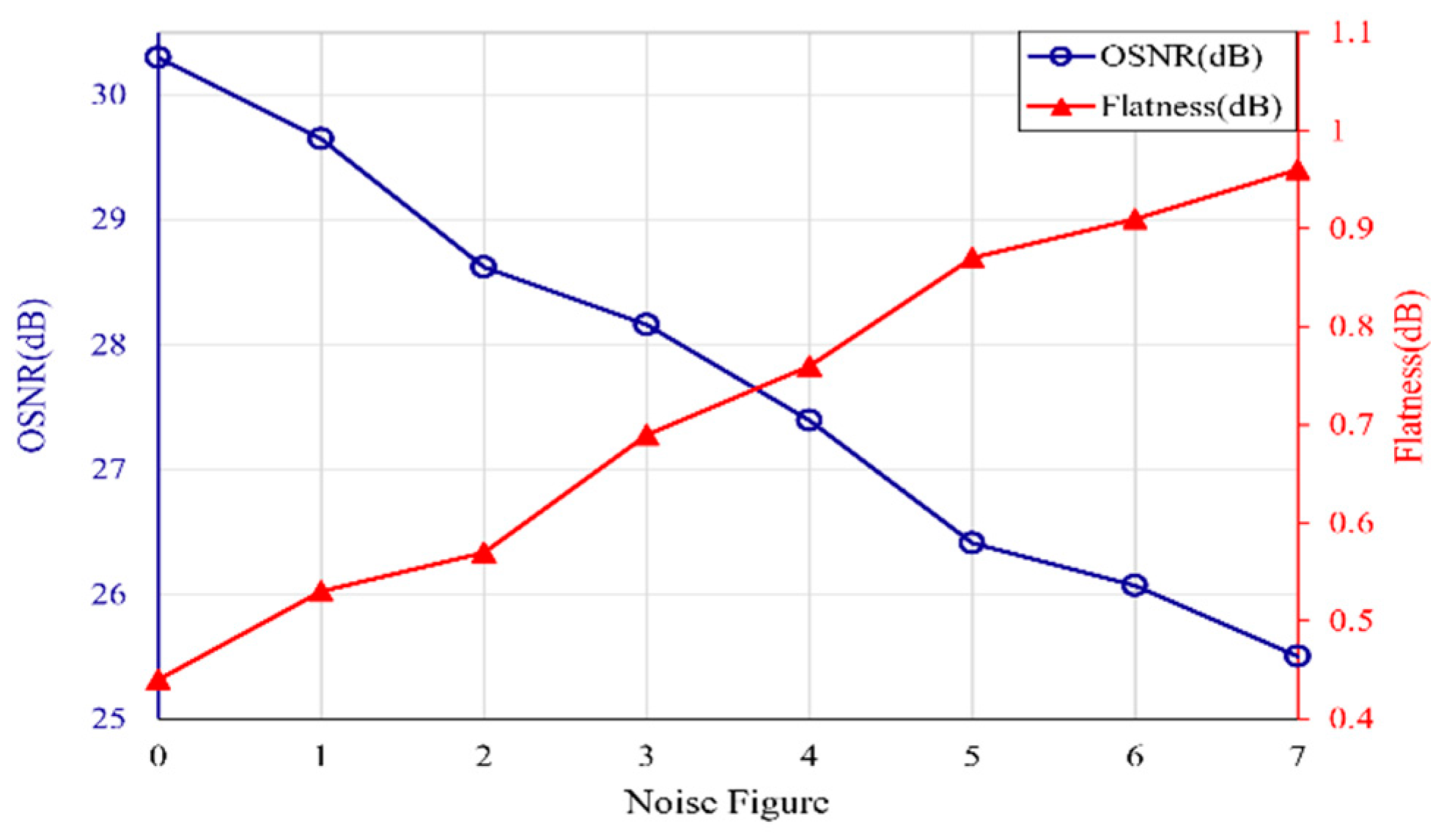
Noise figure is also an important parameter in EDFA; it has an influence on the generated optical frequency comb; here, taking the generation of 111-line optical frequency comb as an example as before to analyze the influence of noise figure on the flatness and OSNR of the generated optical frequency comb.
Figure 6 shows the variation curves of OSNR and the flatness of the comb lines under different noise figures. It can be found that with the increase in the noise figure, the OSNR of the generated optical frequency comb will decrease. The noise figure also causes power fluctuation of comb lines, which makes the flatness worse. In the simulation, when the noise figure varies from 0 to 7, the OSNR will decrease from 30.3 dB to 25.5 dB, and the flatness will become poor from 0.46 dB to 0.96 dB. Compared with Ref. [
19], when the noise figure varies from 0 to 7, the fluctuation ranges of both OSNR and flatness in this paper are relatively small, which means that the system of the proposed scheme has somewhat improved on the performance of noise-immune.
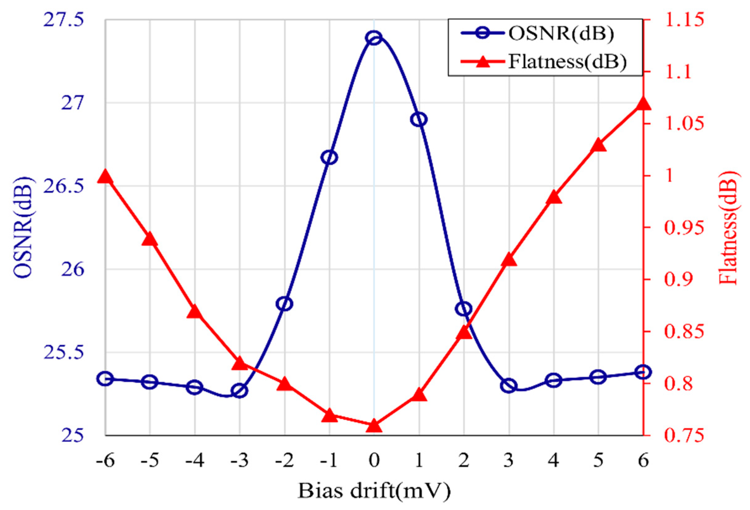
DDMZMs are important devices in the generation system, and the DC biases applied to the modulators need to be precisely controlled, but the DC bias voltages may deviate from the ideal values in the practice situation due to ambient temperature change. The above simulations are based on the ideal situation in that the DC bias voltages of the modulators are at the correct values. Therefore, it is necessary to analyze the influence of DC bias drifts on the performance of the generated OFC. For the sake of convenience, taking the generation of 111-line optical frequency comb as an example as before to analyze the influence of the DC bias drifts on the OSNR and flatness of the comb lines. In the simulation, the drift range of DC bias voltage is set to −6 mV~6 mV. The simulation result is shown in
Figure 7.
It is observed from
Figure 7 that when the bias voltage is set according to the theoretical value, i.e., the DC bias drift is 0, the OSNR of the optical frequency comb is the largest, and the flatness of the comb lines is the best. When DC biases deviate from the ideal value by 6 mV, the flatness of the comb lines is 1.07 dB, which differs from the optimal flatness by about 0.31 dB, and the OSNR falls about 2 dB. It can be seen that DC bias drifts have an effect on the performance of the generated optical frequency comb, but within a small drift range, the effect is small. In Ref. [
19], the variation of flatness and OSNR of the generated 111-line OFC is about 0.29 dB and 1.95 dB, respectively, which means that the system of the proposed scheme and the system in Ref. [
19] have similar stability.


