Double Heterojunction Crystalline Silicon Solar Cells: From Doped Silicon to Dopant-Free Passivating Contacts

Abstract

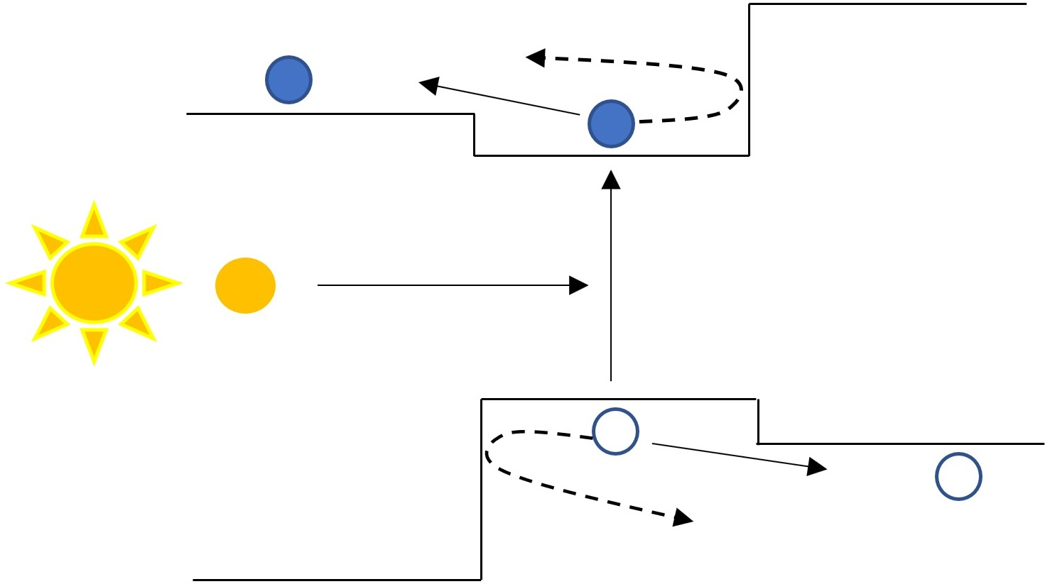
1. Introduction
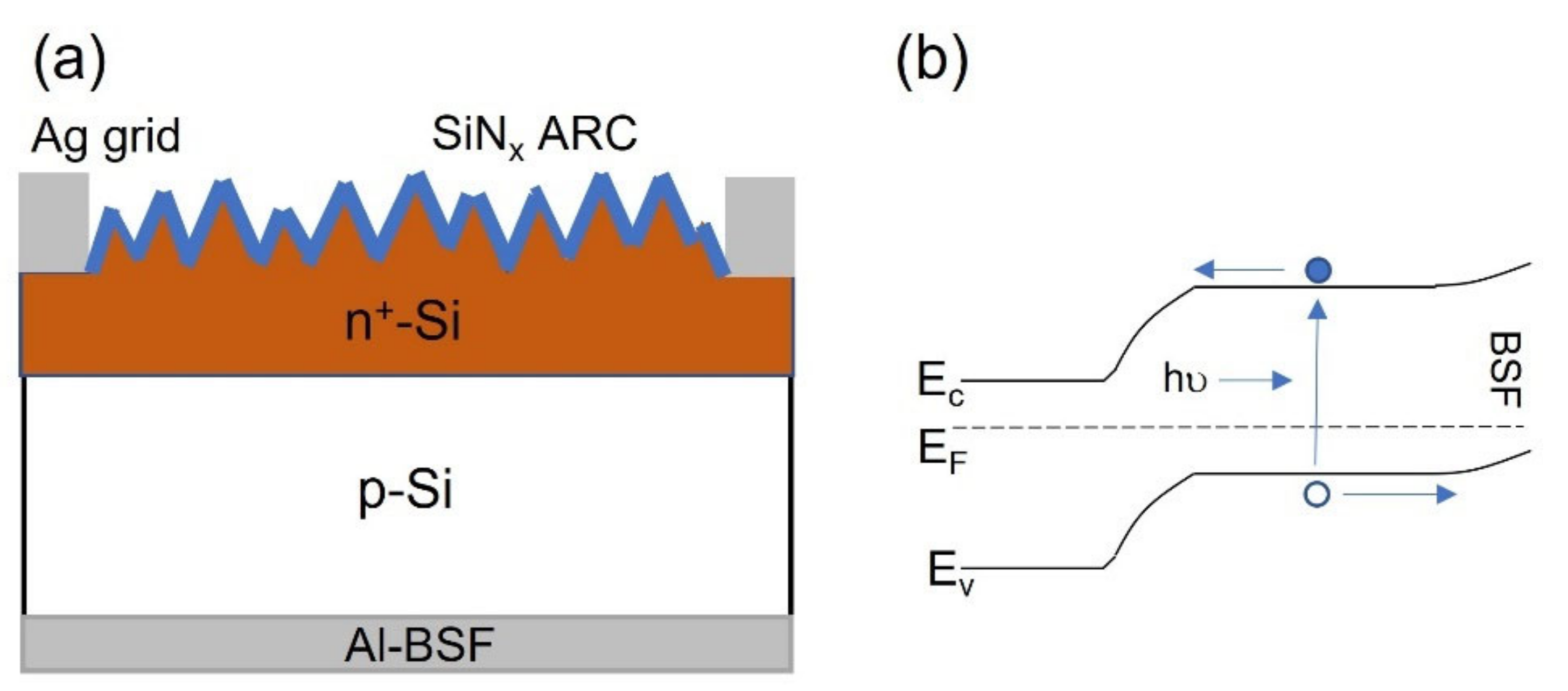
2. Diffused Homojunction Carrier Selective Contacts
3. Passivating Contacts Involving Doped Si
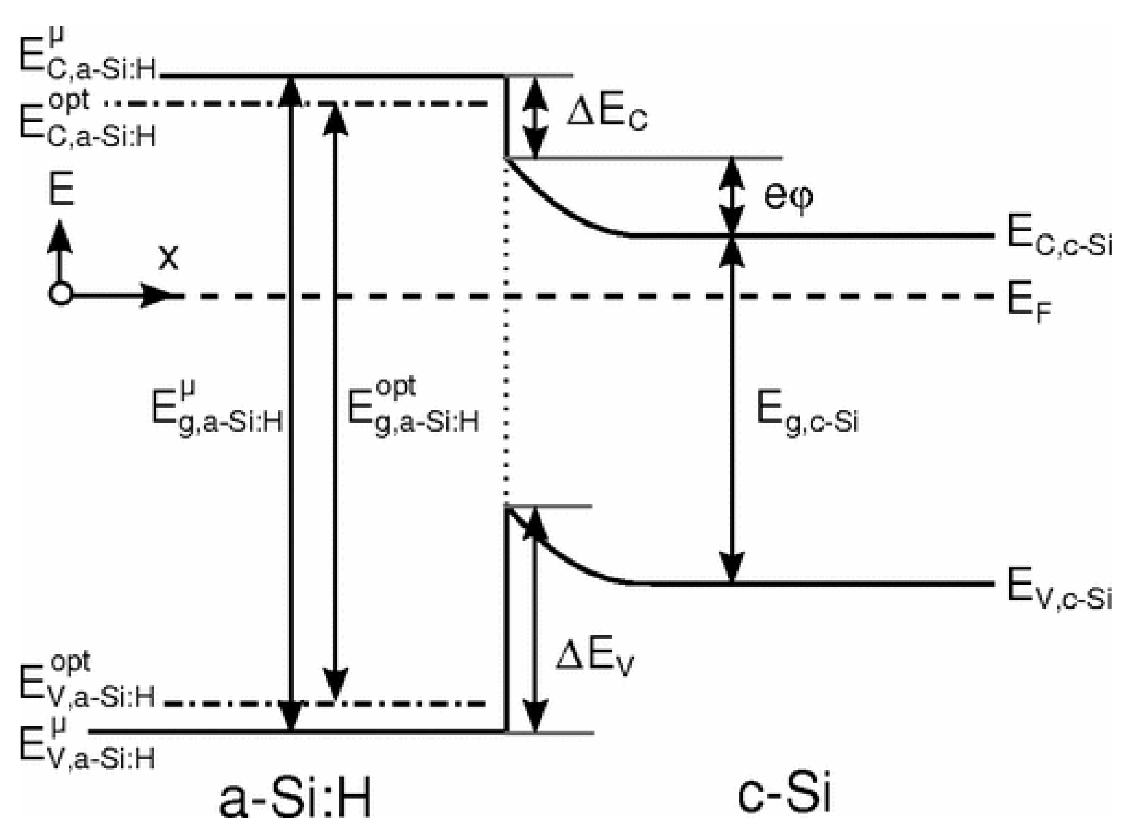
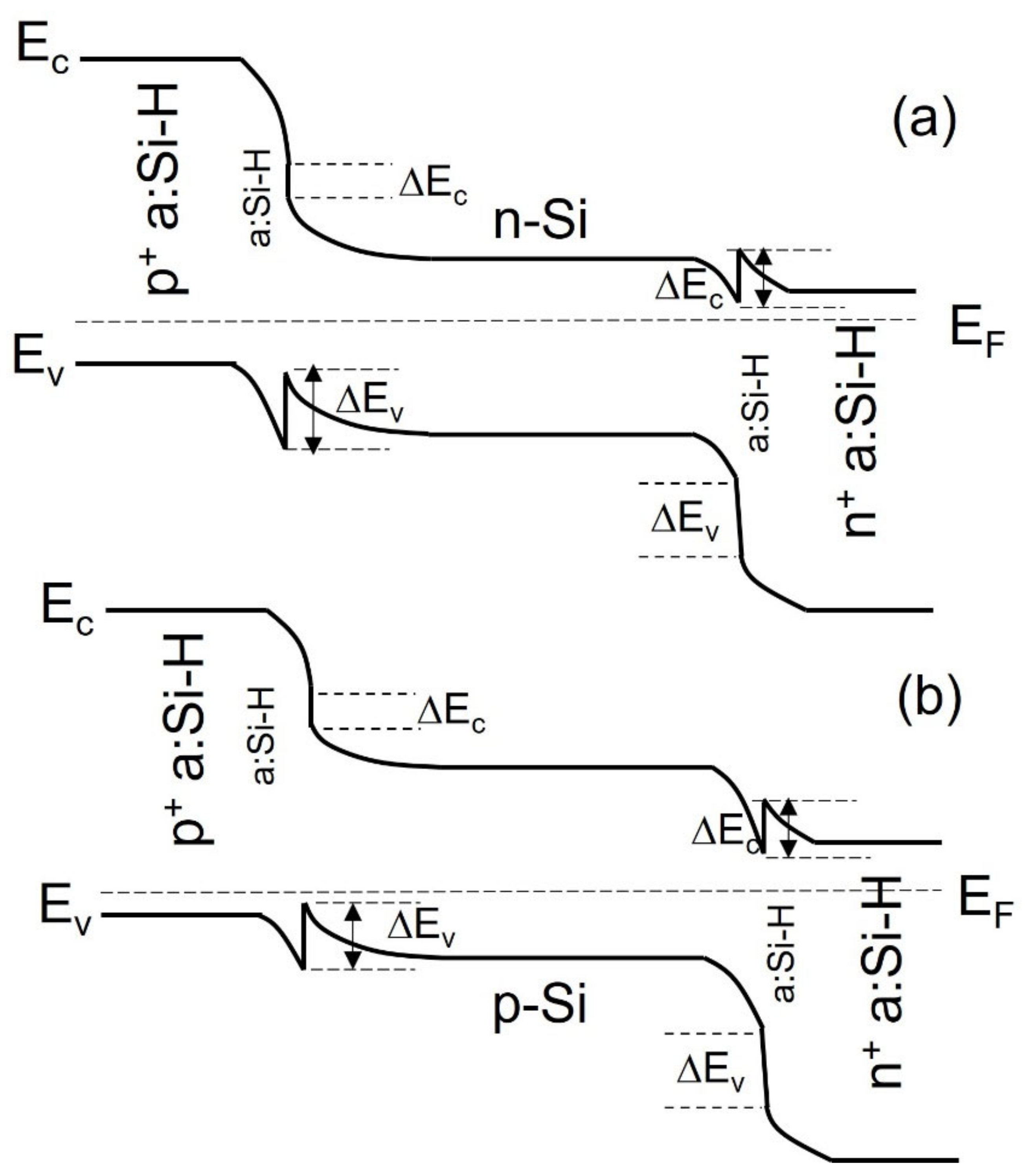
3.1. Silicon Heterojunction
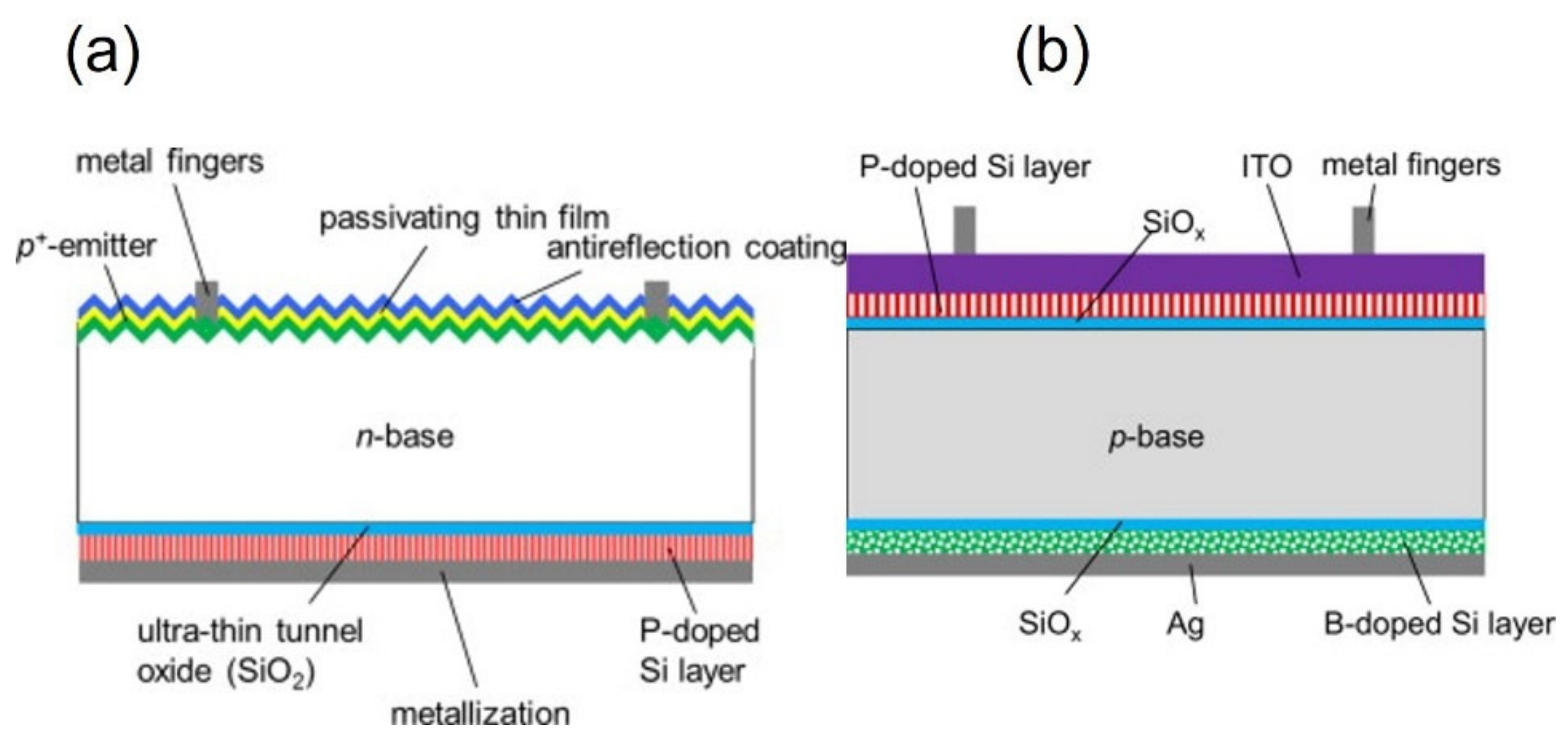
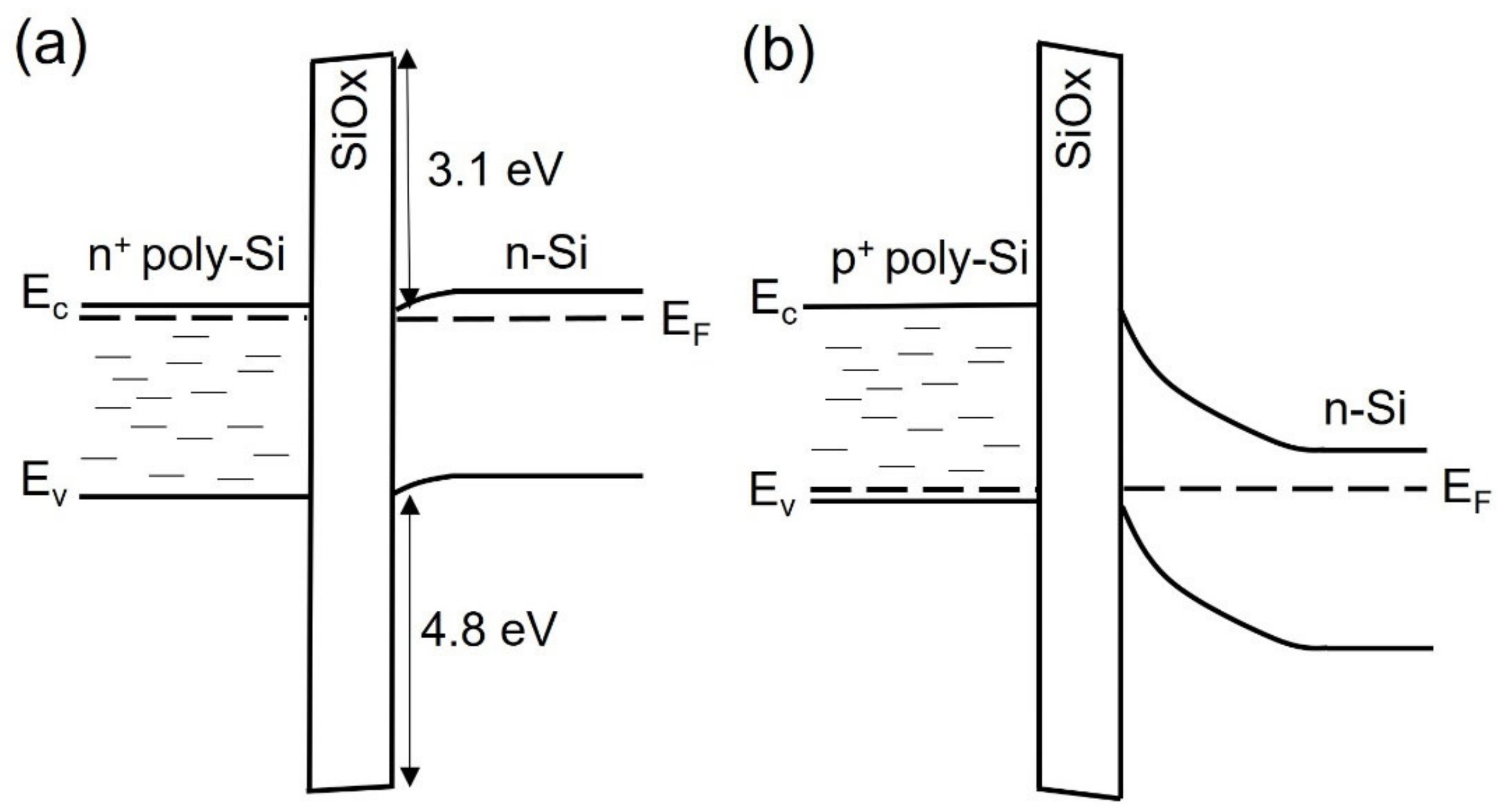
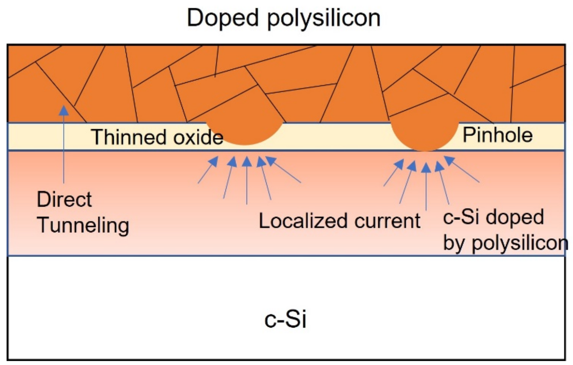
3.2. Polysilicon on Oxide
4. Dopant-Free Passivating Contacts
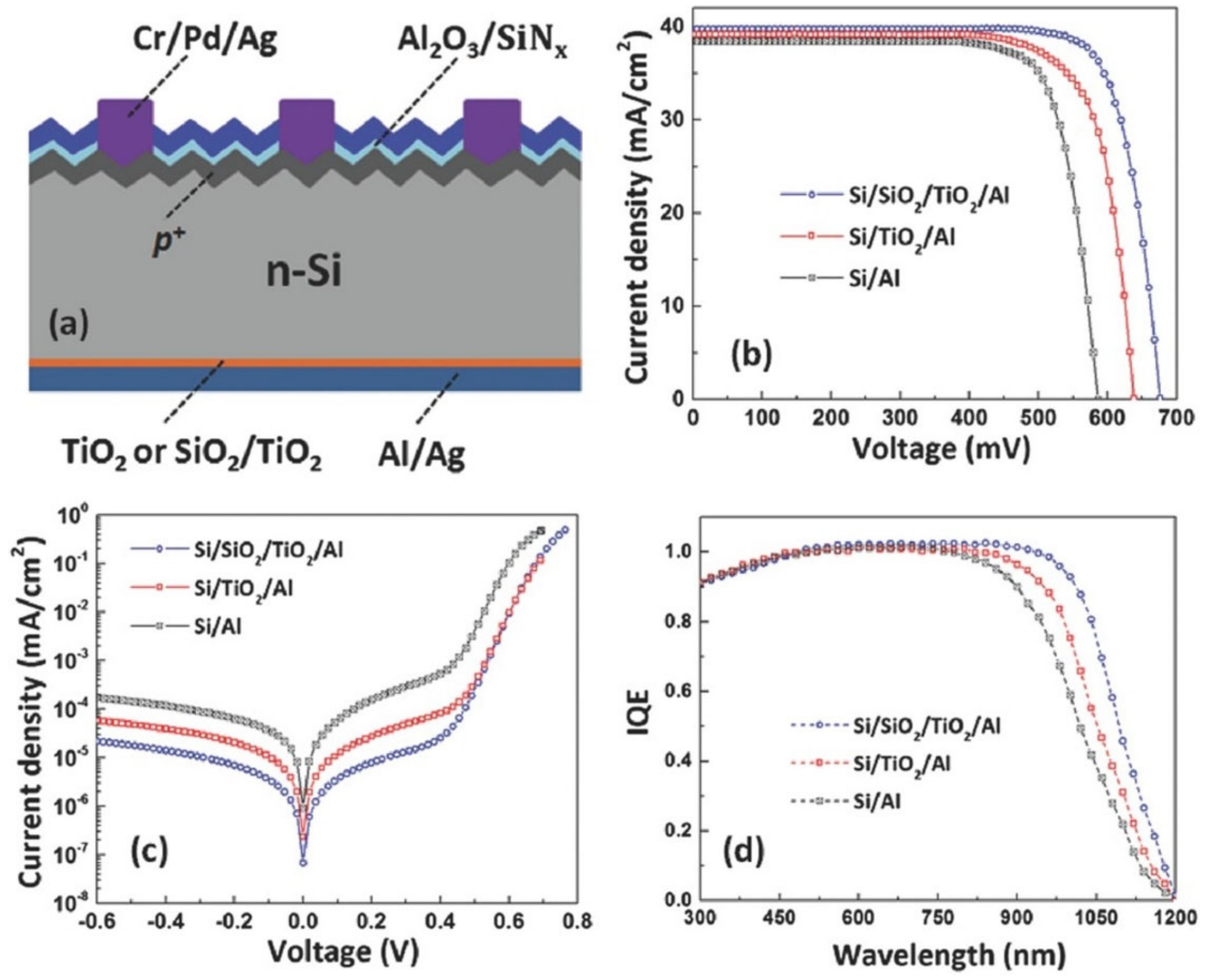
4.1. Titanium Oxide
4.2. Magnesium Oxide
4.3. Lithium Fluoride
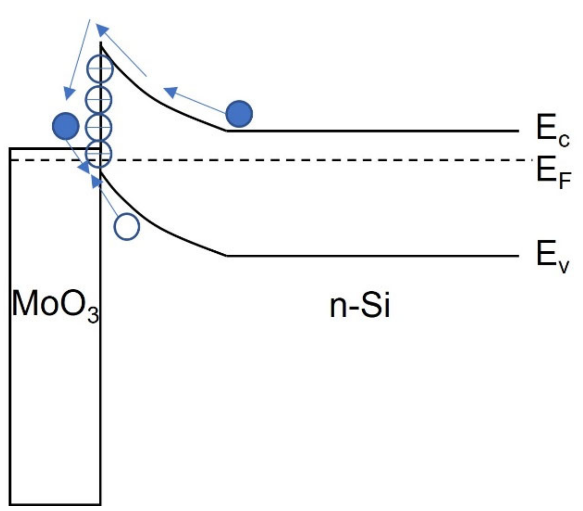
4.4. Molybdenum Oxide
4.5. Other Metal Oxides
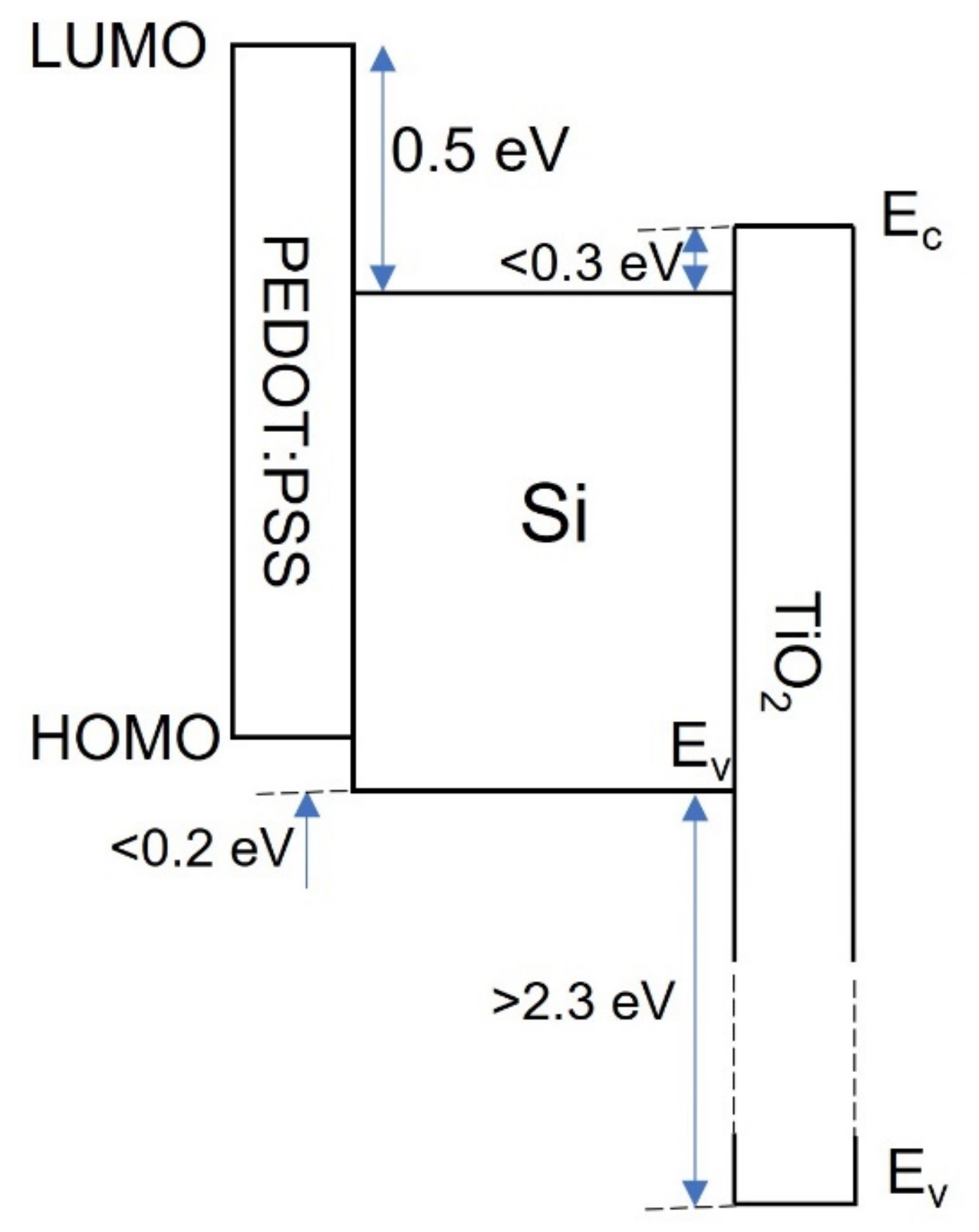
4.6. Organic Passivating Contacts
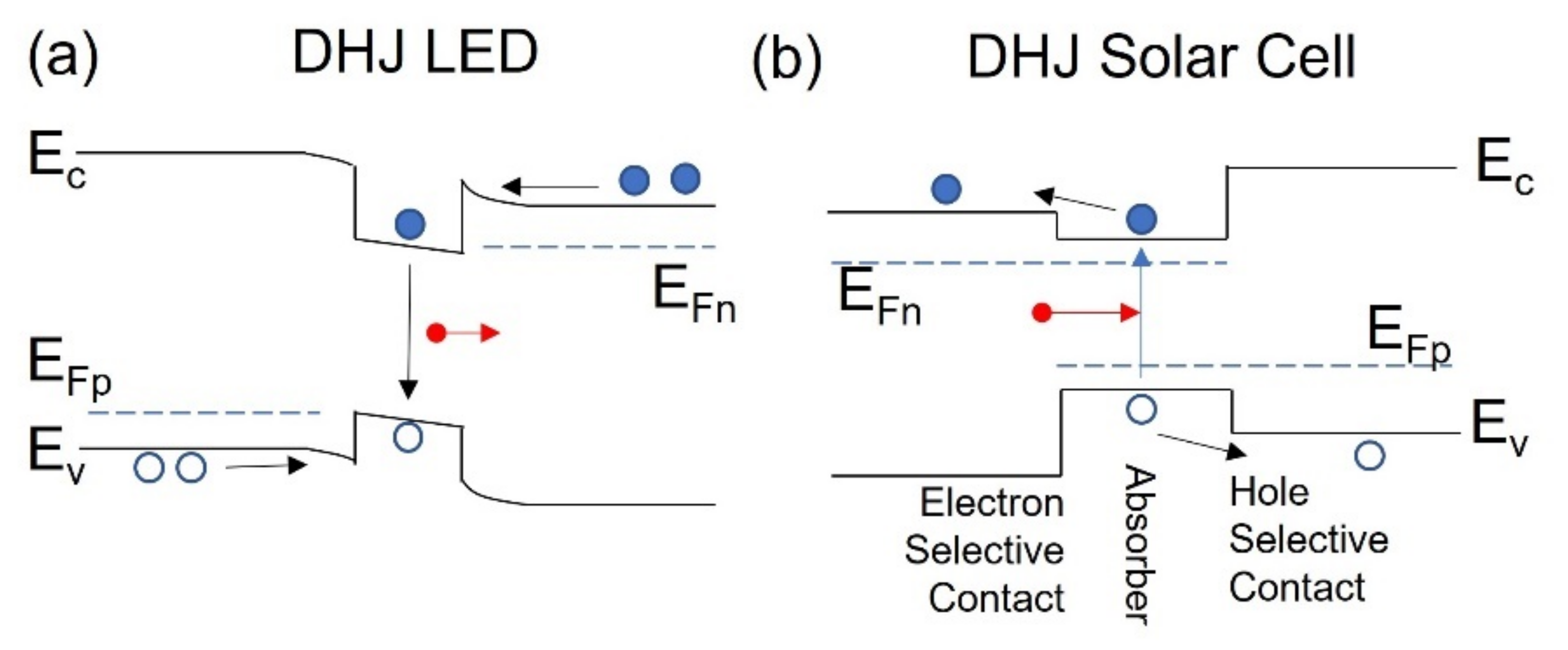
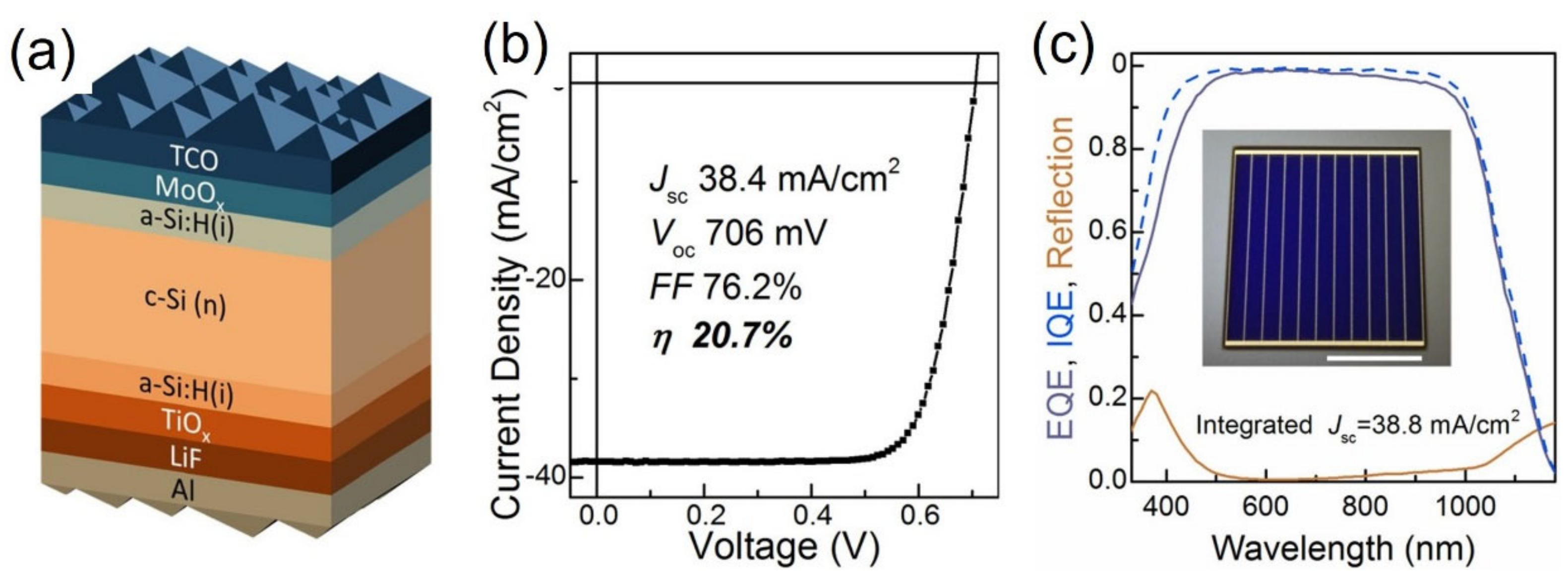
5. DHJ c-Si Solar Cells
6. Challenges and Outlook
Author Contributions
Funding
Conflicts of Interest
References
- Masters, G.M. Renewable and Efficient Electric Power Systems; Wiley-Interscience: Hoboken, NJ, USA, 2004; pp. 445–447. [Google Scholar]
- Twidell, J.; Weir, T. Renewable Energy Resources; Taylor and Francis: Abingdon, UK, 2010; pp. 85–114. [Google Scholar]
- World Energy Outlook; International Energy Agency, IEA Publications: Paris, France, 2021; p. 124.
- Lewis, N.S. Towards cost-effective solar energy use. Science 2007, 315, 798–801. [Google Scholar] [CrossRef] [PubMed]
- Renewables 2021 Global Status Report; REN21, c/o UN Environment Programme; REN21: Paris, France, 2021; pp. 117–118.
- Polman, A.; Knight, M.; Garnett, E.C.; Ehrler, B.; Sinke, W.C. Photovoltaic materials: Present efficiencies and future challenges. Science 2016, 352, aad4424. [Google Scholar] [CrossRef] [PubMed]
- Green, M.A. Silicon photovoltaic modules: A brief history of the first 50 years. Prog. Photovolt. Res. Appl. 2005, 13, 447–455. [Google Scholar] [CrossRef]
- Goetzberger, A.; Hebling, C.; Schock, H.-W. Photovoltaic materials, history, status and outlook. Mater. Sci. Eng. R 2003, 40, 1–46. [Google Scholar] [CrossRef]
- Adachi, S. Earth-Abundant Materials for Solar Cells; Wiley: Chichester, UK, 2015; pp. 2–3. [Google Scholar]
- Aberle, A.G. Crystalline Silicon Solar Cells Advanced Surface Passivation and Analysis; University of New South Wales: Syndey, Australia, 2009; pp. 13–46. [Google Scholar]
- Glunz, S.W. High-efficiency crystalline silicon solar cells. Adv. Optoelectr. 2007, 2007, 97370. [Google Scholar] [CrossRef] [PubMed]
- Green, M.A.; Dunlop, E.D.; Hohl-Ebinger, J.; Yoshita, M.; Kopidakis, N.; Hao, X. Solar cell efficiency tables (version 59). Prog. Photovolt. Res. Appl. 2022, 30, 3–12. [Google Scholar] [CrossRef]
- Richter, A.; Hermle, M.; Glunz, S. Reassessment of the limiting efficiency of crystalline silicon solar cells. IEEE J. Photovolt. 2013, 4, 1184–1191. [Google Scholar] [CrossRef]
- Muller, A.; Ghosh, M.; Sonnenschein, R.; Woditsch, P. Silicon for photovoltaic applications. Mater. Sci. Eng. B 2006, 134, 257–262. [Google Scholar] [CrossRef]
- De Wolf, S.; Descoeudres, A.; Holman, Z.C.; Ballif, C. High-efficiency silicon heterojunction solar cells: A review. Green 2012, 2, 7–24. [Google Scholar] [CrossRef]
- Allen, T.G.; Bullock, J.; Yang, X.; Javey, A.; De Wolf, S. Passivating contacts for crystalline silicon solar cells. Nat. Energy 2019, 4, 914–928. [Google Scholar] [CrossRef]
- Hermle, M.; Feldmann, F.; Bivour, M.; Goldschmidt, J.C.; Glunz, S.W. Passivating contacts and tandem concepts: Approaches for the highest silicon-based solar cell efficiencies. Appl. Phys. Rev. 2020, 7, 021305. [Google Scholar] [CrossRef]
- Wurfel, P.; Wurfel, U. Physics of Solar Cells: From Basic Principles to Advanced Concepts; Wiley-VCH: Weinheim, Germany, 2009. [Google Scholar]
- Tsakalakos, L. Introduction to photovoltaic physics, applications, and technologies. In Nanotechnology for Photovoltaics; Tsakalakos, L., Ed.; CRC Press: Boca Raton, FL, USA, 2010; pp. 1–48. [Google Scholar]
- Sze, S.M.; Lee, M.K. Semiconductor Devices physics and Technology, 3rd ed.; Wiley: Singapore, 2013; pp. 123–127. [Google Scholar]
- Green, M.A. Crystalline silicon solar cells. In Clean Electricity from Photovoltaics; Archer, M.D., Hill, R., Eds.; Imperial College Press: London, UK, 2005; pp. 149–198. [Google Scholar]
- Taur, Y.; Ning, T.H. Section 8.3 Parasitic Elements. In Fundamentals of Modern VLSI Devices, 2nd ed.; Cambridge University Press: Singapore, 2010; pp. 322–325. [Google Scholar]
- Wenham, S.; Green, M.A.; Watt, M.E.; Corkish, R.; Sproul, A. Applied Photovoltaics, 3rd ed.; Earthscan: Abingdon, UK, 2011; pp. 41–44. [Google Scholar]
- Sze, S.M.; Li, Y.; Ng, K.K. Section 1.5 Carrier-Transport Phenomena. In Physics of Semiconductor Devices, 4th ed.; Wiley: Hoboken, NJ, USA, 2021; pp. 37–43. [Google Scholar]
- Shockley, W.; Queisser, H.J. Detailed balance limit of efficiency of p-n junction solar cells. J. Appl. Phys. 1961, 32, 510–519. [Google Scholar] [CrossRef]
- Hezel, R. Recent progress in MIS solar cell. Prog. Photovolt. Res. Appl. 1997, 5, 109–120. [Google Scholar] [CrossRef]
- Schmidt, J.; Peibst, R.; Brendel, R. Surface passivation of crystalline silicon solar cells. Sol. Energy Mater. Sol. Cells 2018, 187, 39–54. [Google Scholar] [CrossRef]
- Hoex, B.; Schmidt, J.; Bock, R.; Altermatt, P.P.; van de Sanden, M.C.M.; Kessels, W.M.M. Excellent passivation of highly doped p-type Si surfaces by the negative-charge-dielectric Al2O3. Appl. Phys. Lett. 2007, 91, 112107. [Google Scholar] [CrossRef]
- Blakers, A.; Wang, A.; Milne, A.M.; Zhao, J.; Green, M.A. 22.8% efficient silicon solar cell. Appl. Phys. Lett. 1989, 55, 1363–1365. [Google Scholar] [CrossRef]
- Zhao, J.; Wang, A.; Altermatt, P.; Green, M.A. Twenty-four percent efficient silicon solar cells with double layer antireflection coatings and reduced resistance loss. Appl. Phys. Lett. 1995, 66, 3636–3638. [Google Scholar] [CrossRef]
- Zhao, J.; Wang, A.; Green, M.A. 24.5% efficiency silicon PERT cells on MCZ substrates and 24.7% efficiency PERL cells on FZ substrates. Prog. Photovolt. Res. Appl. 1999, 7, 471–474. [Google Scholar] [CrossRef]
- Green, M.A. The path to 25% silicon solar cell efficiency: History of silicon cell evolution. Prog. Photovolt. Res. Appl. 2009, 17, 183–189. [Google Scholar] [CrossRef]
- Masuko, K.; Shigematsu, M.; Hashiguchi, T.; Fujishima, D.; Kai, M.; Yoshimura, N.; Yamaguchi, T.; Ichihashi, Y.; Mishima, T.; Matsubara, N.; et al. Achievement of more than 25% conversion efficiency with crystalline silicon heterojunction solar cell. IEEE J. Photovolt. 2014, 4, 1433–1435. [Google Scholar] [CrossRef]
- Yablonovitch, E.; Gmitter, T.; Swanson, R.M.; Kwark, Y.H. A 720 mV open circuit voltage SiOx:c-Si:SiOx double heterostructure solar cell. Appl. Phys. Lett. 1985, 47, 1211–1213. [Google Scholar] [CrossRef]
- Sze, S.M.; Li, Y.; Ng, K.K. Section 12.3 Light-Emitting Diode (LED). In Physics of Semiconductor Devices, 4th ed.; Wiley: Hoboken, NJ, USA, 2021; p. 704. [Google Scholar]
- Hermle, M. Passivated contacts. In Photovoltaic Solar Energy: From Fundamentals to Applications, 1st ed.; Wiley: Chichester, UK, 2017; pp. 125–135. [Google Scholar]
- Yang, X.; Weber, K.; Hameiri, Z.; De Wolf, S. Industrially feasible, dopant-free, carrier-selective contacts for high-efficiency silicon solar cells. Prog. Photovolt. Res. Appl. 2017, 25, 896–904. [Google Scholar] [CrossRef]
- Sinton, R.A.; Cuevas, A. Contactless determination of current-voltage characteristics and minority-carrier lifetimes in semiconductors from quasi-steady-state photoconductance data. Appl. Phys. Lett. 1996, 69, 2510–2512. [Google Scholar] [CrossRef]
- Cox, R.H.; Strack, H. Ohmic contacts for GaAs devices. Sol. State. Electron. 1967, 10, 1213–1218. [Google Scholar] [CrossRef]
- Schroder, D.K. Semiconductor Material and Device Characterization, 3rd ed.; Wiley Inter-Science: Hoboken, NJ, USA, 2006; pp. 138–149. [Google Scholar]
- Pankove, J.I.; Tarng, M.L. Amorphous silicon as a passivant for crystalline silicon. Appl. Phys. Lett. 1979, 34, 156. [Google Scholar] [CrossRef]
- Zanzucchi, P.J.; Wronski, C.R.; Carlson, D.E. Optical and photoconductive properties of discharge-produced amorphous silicon. J. Appl. Phys. 1977, 48, 5227–5288. [Google Scholar] [CrossRef]
- Taguchi, M.; Tanaka, M.; Matsuyama, T.; Matsuoka, T.; Tsuda, S.; Nakano, S.; Kishi, Y.; Kuwano, Y. Improvement of the Conversion Efficiency of Polycrystalline Silicon Thin Film Solar Cell. In Proceedings of the International Photovoltaic Science and Engineering Conference PVSEC-5 Technical Digest, Kyoto, Japan, 26–30 November 1990; pp. 689–692. [Google Scholar]
- Taguchi, M.; Yano, A.; Tohoda, S.; Matsuyama, K.; Nakamura, Y.; Nishiwaki, T.; Fujita, K.; Maruyama, E. 24.75 record efficiency HIT solar cell on thin silicon wafer. IEEE J. Photovolt. 2014, 4, 96–99. [Google Scholar] [CrossRef]
- Yoshikawa, K.; Kawasaki, H.; Yoshida, W.; Irie, T.; Konishi, K.; Nakano, K.; Uto, T.; Adachi, D.; Kanesatsu, M.; Uzu, H.; et al. Silicon heterojunction solar cell with interdigitated back contacts for a photoconversion efficiency over 26%. Nat. Energy 2017, 2, 17032. [Google Scholar] [CrossRef]
- Schulze, T.F.; Korte, L.; Ruske, F.; Rech, B. Band lineup in amorphous/crystalline silicon heterojunctions and the impact of hydrogen microstructure and topological disorder. Phys. Rev. B 2011, 83, 165314. [Google Scholar] [CrossRef]
- Korte, L.; Schmidt, M. Doping type and thickness dependence of band offsets at the amorphous/crystalline silicon heterojunction. J. Appl. Phys. 2011, 109, 063717. [Google Scholar] [CrossRef]
- Heilig, K. Determination of doping factor, mobility ratio and excess concentration using photovoltages at extreme band bending. Solid-State Electron. 1978, 21, 975. [Google Scholar] [CrossRef]
- Descoeudres, A.; Homan, Z.C.; Barraud, L.; Morel, S.; De Wolf, S.; Ballif, C. >21% efficient silicon heterojunction solar cells on n- and p-type wafers compared. IEEE J. Photovolt. 2013, 3, 83–89. [Google Scholar] [CrossRef]
- De Wolf, S.; Kondo, M. Boron-doped a-i:H/c-Si interface passivation: Degradation mechanism. Appl. Phys. Lett. 2007, 91, 112109. [Google Scholar] [CrossRef]
- Romer, U.; Peibst, R.; Ohrdes, T.; Lim, B.; Krugener, J.; Wietler, T.; Brendel, R. Ion implantation for poly-silicon passivated back-junction back-contacted solar cells. IEEE J. Photovolt. 2015, 5, 507–514. [Google Scholar] [CrossRef]
- Romer, U.; Peibst, R.; Ohrdes, T.; Lim, B.; Krugener, J.; Bugiel, E.; Brendel, R. Recombination behavior and contact resistance of n+ and p+ poly-crystalline and mono-crystalline silicon junctions. Sol. Mater. Energy Sol. Cells 2014, 131, 85–91. [Google Scholar] [CrossRef]
- Feldmann, F.; Bivour, M.; Reichel, C.; Hermle, M.; Glunz, S.W. Passivated rear contacts for high efficiency n-type silicon solar cells providing high interface passivation quality and excellent transport characteristics. Sol. Mater. Energy Sol. Cells 2014, 120, 270–274. [Google Scholar] [CrossRef]
- Taur, Y.; Ning, T.H. Section 9.2 Ideal Current–Voltage Characteristics. In Fundamentals of Modern VLSI Devices, 2nd ed.; Cambridge University Press: Singapore, 2010; pp. 376–377. [Google Scholar]
- Tetzlaff, D.; Krugener, J.; Larionova, Y.; Reiter, S.; Turcu, M.; Hasse, F.; Brendel, R.; Peibst, R.; Hohne, U.; Kahler, J.-D.; et al. A simple method for pinhole detection in carrier selective POLO-junctions for high efficiency silicon solar cells. Sol. Energy Mater. Sol. Cells 2017, 173, 106–110. [Google Scholar] [CrossRef]
- Feldmann, F.; Simon, M.; Bivour, M.; Reichel, C.; Hermle, M. Efficient carrier-selective p- and n-contacts for Si solar cells. Sol. Energy Mater. Sol. Cells 2014, 131, 100–104. [Google Scholar] [CrossRef]
- Richter, A.; Benick, J.; Feldmann, F.; Fell, A.; Hermle, M.; Glunz, S.A. N-Type Si solar cells with passivated electron contact: Identifying sources for efficiency improvement by wafer thickness and resistivity variation. Sol. Energy Mater. Sol. Cells 2017, 173, 96–105. [Google Scholar] [CrossRef]
- Yang, G.; Guo, P.; Procel, P.; Limodio, G.; Weeber, A.; Isabella, O.; Zeman, M. High-efficiency black IBC c-Si solar cells with poly-Si as carrier-selective passivating contacts. Sol. Energy Mater. Sol. Cells 2018, 186, 9–13. [Google Scholar] [CrossRef]
- Hollemann, C.; Hasse, F.; Schafer, S.; Krugener, J.; Brendel, R.; Peibset, R. 26.1% efficiency POLO-IBC cells: Quantification of electrical and optical loss mechanisms. Prog. Photovolt. Res. Appl. 2019, 27, 950–958. [Google Scholar] [CrossRef]
- Hasse, F.; Holleman, C.; Schafer, S.; Merkle, A.; Rjenacker, M.; Krugener, J.; Brendel, R.; Peibst, R. Laser contact openings for local poly-Si-metal contacts enabling 26.1%-efficient POLO-IBC solar cells. Sol. Energy Mater. Sol. Cells 2018, 186, 184–193. [Google Scholar] [CrossRef]
- Peibst, R.; Romer, U.; Larionova, Y.; Rienacker, M.; Merkle, A.; Folchert, N.; Reiter, S.; Turcu, M.; Min, B.; Krugener, J.; et al. Working principle of carrier selective poly-Si/c-Si junctions: Is tunnelling the whole story? Sol. Energy Mater. Sol. Cells 2016, 158, 60–67. [Google Scholar] [CrossRef]
- Richter, S.; Larionova, Y.; Grober, S.; Menzel, M.; Schulte-Huxel, H.; Peibst, R.; Brendel, R.; Hagendorf, C. Evaluation of Localized Vertical Current Formation in Carrier Selective Passivation Layers of Silicon Solar Cells by Conductive AFM. In AIP Conference Proceedings, Proceedings of SiliconPV 2019, Leuven, Belgium, 8–10 April 2019; AIP Publishing LLC: Melville, NY, USA, 2019; Volume 2147, p. 040017. [Google Scholar]
- Mewe, A.; Stodolny, M.; Anker, J.; Lenes, M.; Pages, X.; Wu, Y.; Tool, K.; Geerligs, B.; Romijn, I. Full Wafer Size Ibc Cell with Polysilicon Passivating Contacts. In AIP Conference Proceedings, Proceedings of SiliconPV 2018, Lausanne, Switzerland, 19–21 March 2018; AIP Publishing LLC: Melville, NY, USA, 2019; Volume 1999, p. 040014. [Google Scholar]
- Liu, C.; Chen, D.; Chen, Y.; Yuan, L.; Yang, Z.; Yao, W.; Gong, J.; Feng, Z.; Altermatt, P.P.; Verlinde, P.J. Industrial TOPCon solar cells on n-type quasi-mono Si wafers with efficiencies above 23%. Sol. Energy Mater. Sol. Cells 2020, 215, 110690. [Google Scholar] [CrossRef]
- Chen, Y.; Chen, D.; Liu, C.; Wang, Z.; Zou, Y.; He, Y.; Wang, Y.; Yuan, L.; Gong, J.; Lin, W.; et al. Mass production of industrial tunnel oxide passivated contacts (i-TOPCon) silicon solar cells with average efficiency over 23% and modules over 345W. Prog. Photovolt. Res. Appl. 2019, 27, 827–834. [Google Scholar] [CrossRef]
- Chen, D.; Chen, Y.; Wang, Z.; Gong, J.; Liu, C.; Zou, Y.; He, Y.; Wang, Y.; Yuan, L.; Lin, W.; et al. 24.58% total area efficiency of screen-printed, large area industrial silicon solar cells with the tunnel oxide passivated contacts (i-TOPCon) design. Sol. Energy Mater. Sol. Cells 2020, 206, 110258. [Google Scholar] [CrossRef]
- Tsuijmura, T. OLED Display Fundamentals and Applications, 2nd ed.; Wiley-SID: Hoboken, NJ, USA, 2017; pp. 61–67. [Google Scholar]
- Lane, P.A.; Kafafi, Z.H. Solid-state organic photovoltaics: A review of molecular and polymeric devices. In Organic Photovoltaics Mechanisms, Materials, and Devices; Sun, S.-S., Sariciftci, N.S., Eds.; CRC Taylor and Francis: Boca Raton, FL, USA, 2005; pp. 49–104. [Google Scholar]
- Wong, T.K.S. Effect of embedded nanoparticle surface chemistry on plasmonic organic photovoltaic devices. Mater. Renew. Sustain. Energy 2017, 6, 4. [Google Scholar] [CrossRef][Green Version]
- Zhuk, S.; Wong, T.K.S.; Petrovit, M.; Kymakis, E.; Hadke, S.S.; Lie, S.; Wong, L.H.; Sonar, P.; Dey, A.; Krishnamurthy, S.; et al. Solution processed pure sulfide Cu2[Zn0.6Cd0.4]SnS4 solar cells with efficiency of 10.8% using ultrathin CuO intermediate layer. Sol. RRL 2020, 4, 2000293. [Google Scholar] [CrossRef]
- Nazeeruddin, M.K.; Snaith, H. Methylammonium triiode perovskite solar cells: A new paradigm in photovoltaics. MRS Bull. 2015, 40, 641–645. [Google Scholar] [CrossRef]
- Meyer, J.; Hamwi, S.; Kroger, M.; Kowalsky, W.; Riedl, T.; Kahn, A. Transition metal oxides for organic electronics: Energetics, device physics and applications. Adv. Mater. 2012, 24, 5408–5427. [Google Scholar] [CrossRef]
- Elschner, A.; Kirchmeyer, S.; Lowenich, W.; Merker, U.; Reuter, K. PEDOT: Principles and Applications of an Intrinsically Conductive Polymer; CRC Press: Boca Raton, FL, USA, 2011. [Google Scholar]
- Card, H.C. Aluminum-silicon Schottky barriers and ohmic contacts in integrated circuits. IEEE Trans. Electron Dev. 1976, 23, 538–544. [Google Scholar] [CrossRef]
- Kim, H.; Ou, K.-L.; Wu, X.; Ndione, P.F.; Berry, J.; Lambert, Y.; Melin, T.; Armstrong, N.R.; Graham, S. Investigation of ultra-thin titania films as hole-blocking contacts for organic photovoltaics. J. Mater. Chem. A 2015, 3, 17332. [Google Scholar] [CrossRef]
- Liao, B.; Hoex, B.; Aberle, A.G.; Chi, D.; Bhatia, C.S. Excellent c-Si surface passivation by low-temperature atomic layer deposited titanium oxide. Appl. Phys. Lett. 2014, 104, 253903. [Google Scholar] [CrossRef]
- Thomson, A.F.; McIntosh, K.R. Light-enhanced surface passivation of TiO2-coated silicon. Prog. Photovolt. Res. Appl. 2012, 20, 343–349. [Google Scholar] [CrossRef]
- Avasthi, S.; McClain, W.E.; Man, G.; Kahn, A.; Schwartz, J.; Sturm, J.C. Hole-Blocking titanium oxide/silicon heterojunction and its application to photovoltaics. Appl. Phys. Lett. 2013, 102, 203901. [Google Scholar] [CrossRef]
- Yang, X.; Bi, Q.; Ali, H.; Davis, K.; Schoenfeld, W.V.; Weber, K. High-performance TiO2-based electron-selective contacts for crystalline silicon solar cell. Adv. Mater. 2016, 28, 5891–5897. [Google Scholar] [CrossRef]
- Taurian, O.E.; Springborg, M.; Christensen, N.E. Self-consistent electronic structures of MgO and SrO. Solid State Commun. 1985, 55, 351–355. [Google Scholar] [CrossRef]
- Choi, H.W.; Kim, S.Y.; Kim, W.-K.; Lee, J.-L. Enhancement of electron injection in inverted top-emitting organic light-emitting diodes using an insulating magnesium oxide buffer layer. Appl. Phys. Lett. 2005, 87, 082102. [Google Scholar] [CrossRef]
- Wan, Y.; Samundsett, C.; Bullock, J.; Hettick, M.; Allen, T.; Yan, D.; Peng, J.; Wu, Y.; Cui, J.; Javey, A.; et al. Conductive and stable magnesium oxide electron-selective contacts for efficient silicon solar cells. Adv. Energy Mater. 2017, 7, 1601863. [Google Scholar] [CrossRef]
- Djurisic, A.B.; Kwong, C.Y. The influence of the electrode choice on the performance of organic solar cells. In Organic Photovoltaics Mechanisms, Materials, and Devices; Sun, S.-S., Sariciftci, N.S., Eds.; CRC Taylor and Francis: Boca Raton, FL, USA, 2005; pp. 453–477. [Google Scholar]
- Bullock, J.; Zheng, P.; Jeangros, Q.; Tosun, M.; Hettick, M.; Sutter-Fella, C.M.; Wan, Y.; Allen, T.; Yan, D.; Macdonald, D.; et al. Lithium fluoride based electron contacts for high efficiency n-type crystalline silicon solar cell. Adv. Energy Mater. 2016, 6, 1600241. [Google Scholar] [CrossRef]
- Bullock, J.; Cuevas, A.; Allen, T.; Battaglia, C. Molybdenum oxide MoOx: A versatile hole contact for silicon solar cell. Appl. Phys. Lett. 2014, 105, 232109. [Google Scholar] [CrossRef]
- Geissbuhler, J.; Werner, J.; de Nicholas, S.M.; Barraud, L.; Hessler-Wyser, A.; Despeisse, M.; Nicolay, S.; Tomasi, A.; Biesen, B.; De Wolf, S.; et al. 22.5% efficient silicon heterojunction solar cell with molybdenum oxide hole collector. Appl. Phys. Lett. 2015, 107, 081601. [Google Scholar] [CrossRef]
- Mallem, K.; Yong, J.K.; Hussain, S.Q.; Duutta, S.; Anh, H.T.L.; Ju, M.; Park, J.; Cho, Y.H.; Kim, Y.; Cho, E.-C.; et al. Molybdenum oxide: A superior hole extraction layer for replacing p-type hydrogenated amorphous silicon with high efficiency heterojunction Si solar cells. Mater. Res. Bull. 2019, 110, 90–96. [Google Scholar] [CrossRef]
- Gregory, G.; Eeit, C.; Gao, Z.; Banerjee, P.; Jurca, T.; Davis, K.O. Improving the passivation of molybdenum oxide hole-selective contacts with 1 nm hydrogenated aluminum oxide films for silicon solar cells. Phys. Stat. Solidi A 2020, 217, 2000093. [Google Scholar] [CrossRef]
- Dreon, J.; Cattin, J.; Christmann, G.; Febba, D.; Paratte, V.; Antognini, L.; Lin, W.; Nicolay, S.; Ballif, C.; Boccard, M. Performance limitations and analysis of silicon heterojunction solar cells using ultrathin MoOx hole-selective contacts. IEEE J. Photovolt. 2021, 11, 1158–1166. [Google Scholar] [CrossRef]
- Behera, G.; Vikram; Kumar, A.; Balasubramanian, K.; Alam, A. First-principles study of the surface passivation effect in Si/MoOx interface. J. Phys. Chem. C 2021, 125, 11513–11523. [Google Scholar] [CrossRef]
- Davis, B.E.; Strandwitz, N.C. Aluminum oxide passivating tunneling interlayers for Molybdenum oxide hole-selective contacts. IEEE J. Photovolt. 2020, 10, 722–728. [Google Scholar] [CrossRef]
- Chen, J.; Liu, C.; Xu, S.; Wang, P.; Ge, X.; Han, B.; Zhang, Y.; Wang, M.; Wu, X.; Xu, L.; et al. Solution processes molybdenum oxide films by low-temperature annealing for improved silicon passivation. Mater. Sci. Semicond. Proc. 2021, 132, 105920. [Google Scholar] [CrossRef]
- Song, H.; Lee, C.; Hyun, J.; Lee, S.-W.; Choi, D.; Pyun, D.; Nam, J.; Jeong, S.-H.; Kim, J.; Bae, S.; et al. Monolithic Perovskite-Carrier Selective Contact Silicon Tandem Solar Cells Using Molybdenum Oxide as a Hole Selective Layer. Energies 2021, 14, 3108. [Google Scholar] [CrossRef]
- Cao, S.; Li, J.; Zhang, J.; Lin, Y.; Lu, L.; Wang, J.; Yin, M.; Yang, L.; Chen, X.; Li, D. Stable MoOx-based heterostructures for p-type crystalline silicon solar cells achieving 20% efficiency. Adv. Funct. Mater. 2020, 30, 2004367. [Google Scholar] [CrossRef]
- Li, J.; Pan, T.; Wang, J.; Cao, S.; Lin, Y.; Boex, B.; Ma, Z.; Lu, L.; Yang, L.; Sun, B.; et al. Bilayer MoOx/CrOx passivating contact targeting highly stable silicon heterojunction solar cells. ACS Appl. Mater. Interfaces 2020, 12, 36778–36786. [Google Scholar] [CrossRef] [PubMed]
- Bhatia, S.; Anthony, A.; Nair, P.R. Unraveling the hole-selective nature of Si/MoOx heterojunction. IEEE J. Photovolt. 2020, 10, 1566–1573. [Google Scholar] [CrossRef]
- Singh, K.; Singh, D.K.; Komarala, V.K. Numerical simulations of carrier-selective contact silicon solar cells: Role of carrier-selective layers electronic properties. J. Comput. Electron. 2021, 20, 1815–1821. [Google Scholar] [CrossRef]
- Gerling, L.G.; Mahato, S.; Morales-Vilches, A.; Masmitja, G.; Ortega, P.; Voz, C.; Alcubilla, R.; Puigdollers, J. Transition metal oxides as hole-selective contacts in silicon heterojunction solar cells. Sol. Energy Mater. Sol. Cells 2016, 145, 109–115. [Google Scholar] [CrossRef]
- Zhang, X.; Wan, Y.; Bullock, J.; Allen, T.; Cuevas, A. Low resistance ohmic contact to p-type silicon via nitrogen-doped copper oxide film. Appl. Phys. Lett. 2016, 109, 052102. [Google Scholar] [CrossRef]
- Macco, B.; Black, L.E.; Melskens, J.; van der Loo, B.W.H.; Berghuis, W.-J.H.; Verheijen, M.A.; Kessels, W.M.M. Atomic-layer deposited Nb2O5 as transparent passivating electron contact for c-Si solar cells. Sol. Energy Mater. Sol. Cells 2014, 184, 98–104. [Google Scholar] [CrossRef]
- Coss, B.E.; Loh, W.-Y.; Wallace, R.M.; Kim, J.; Majhi, P.; Jammy, R. Near band edge Schottky barrier height modulation using high-k dielectric dipole tuning mechanism. Appl. Phys. Lett. 2009, 95, 222105. [Google Scholar] [CrossRef]
- Kita, K.; Toriumi, A. Intrinsic origin of electric dipoles formed at high-k/SiO2 interface. In Proceedings of the Technical Digest: International Electron Devices Meeting, San Francisco, CA, USA, 15–17 December 2008. [Google Scholar]
- Lim, A.E.-J.; Hou, J.; Kwong, D.-L.; Yeo, Y.-C. Manipulating interface dipoles of opposing polarity for work function engineering within a single metal gate stack. In Proceedings of the Technical Digest: International Electron Devices Meeting, San Francisco, CA, USA, 15–17 December 2008. [Google Scholar]
- Nagamatsu, K.A.; Avasthi, S.; Jhaveri, J.; Sturm, J.C. A 12% efficient silicon/PEDOT:PSS heterojunction solar cell fabricated at <100 °C. IEEE J. Photovolt. 2014, 4, 260–265. [Google Scholar] [CrossRef]
- Gagolin, R.; Zielke, D.; Descoeudrs, A.; Despeisse, M.; Ballif, C.; Schmidt, J. Demonstrating the high Voc potential of PEDOT:PSS/c-Si heterojunctions on solar cells. Energy Proc. 2017, 24, 593–597. [Google Scholar] [CrossRef]
- Zielke, D.; Gagolin, R.; Halbich, M.-U.; Marquardt, C.; Lovenich, W.; Sauer, R.; Schmidt, J. Large-area PEDOT:PSS/c-Si heterojunction solar cells with screen-printed metal contacts. Solar RRL 2018, 2, 1700191. [Google Scholar] [CrossRef]
- Nagamatsu, K.A.; Avasthi, S.; Sahasrabudhe, G.; Man, G.; Jhaveri, J.; Berg, A.H.; Schwartz, J.; Kahn, A.; Wagner, S.; Sturm, J.C. Titanium dioxide/silicon hole-blocking selective contact to enable double-heterojunction crystalline silicon-based solar cell. Appl. Phys. Lett. 2015, 106, 123906. [Google Scholar] [CrossRef]
- Bullock, J.; Hettick, M.; Geissbuhler, J.; Ong, A.J.; Allen, T.; Sutter-Fella, C.M.; Chen, T.; Ota, H.; Schaler, E.W.; De Wolf, S.; et al. Efficient silicon solar cells with dopant-free asymmetric heterocontacts. Nat. Energy 2016, 1, 15031. [Google Scholar] [CrossRef]
- Wu, W.; Lin, W.; Zhong, S.; Paviete-Salomon, B.; Despeisse, M.; Liang, Z.; Boccard, M.; Shen, H.; Ballif, C. 22% Efficient Dopant-Free Interdigitated Back Contact Silicon Solar Cells. In AIP Conference Proceedings, Proceedings of SiliconPV 2018, Lausanne, Switzerland, 19–21 March 2018; AIP Publishing LLC: Melville, NY, USA, 2019; Volume 1999, p. 040025. [Google Scholar]
- Nayak, M.; Mudgal, S.; Mandal, S.; Singh, S.; Komarala, V.K. Electrical Characterization and Defect States Analysis of Ag/ITO/MoOx/n-Si/LiFx/Al. AIP Conf. Proc. 2019, 2147, 040014. [Google Scholar]
- Bullock, J.; Wan, Y.; Xu, Z.; Essig, S.; Hettick, M.; Wang, H.; Ji, W.; Boccard, M.; Cuevas, A.; Ballif, C.; et al. Stable dopant-free asymmetric heterocontact silicon solar cells with efficiencies above 20%. ACS Energy Lett. 2018, 3, 508–513. [Google Scholar] [CrossRef]
- Ishii, H.; Sugiyama, K.; Ito, E.; Seki, K. Energy level alignment and interface electronic structures at organic/metal, organic/organic interfaces. Adv. Mater. 1999, 11, 605–625. [Google Scholar] [CrossRef]
- Lu, C. Solution Processed Transition Metal Oxides Selective Contacts for Si Heterojunction Solar Cells. Ph.D. Thesis, Nanyang Technological University, Singapore, 2021. [Google Scholar]


| Electron-Selective Contact | Hole-Selective Contact | PCE (%) | Reference |
|---|---|---|---|
| SHJ | SHJ | 24.7 | [44] |
| SHJ | SHJ | 25.6 | [33] |
| SHJ | SHJ | 26.3 1 | [45] |
| POLO | p+ diffusion | 21.7 | [53] |
| POLO | POLO | 24.4 | [56] |
| POLO | p+ diffusion | 25.7 | [57] |
| POLO | POLO | 23.0 1 | [58] |
| POLO | POLO | 26.1 1 | [59] |
| POLO | p+ diffusion | 23.22 | [64] |
| POLO | p+ diffusion | 23.57 | [65] |
| POLO | p+ diffusion | 24.58 | [66] |
| TiO2 | p+ diffusion | 19.8 | [79] |
| SiO2/TiO2 | p+ diffusion | 21.6 | [79] |
| SiO2/TiO2 | p+ diffusion | 22.1 | [37] |
| MgOx | p+ diffusion | 20.0 | [82] |
| LiFx | p+ diffusion | 20.6 | [84] |
| SHJ | MoOx | 22.5 | [86] |
| Al | PEDOT:PSS | 11.7 | [104] |
| SHJ | PEDOT:PSS | 16.2 | [105] |
| n+ diffusion | PEDOT:PSS | 20.2 | [106] |
| TiO2 | PEDOT:PSS | 11.2 | [107] |
| a-Si:H(i)/LiFx | a-Si:H(i)/MoOx | 19.42 | [108] |
| a-Si:H/MgFx | a-Si:H(i)/MoOx | 22.2 1 | [109] |
| LiFx | MoOx | 15.35 | [110] |
| a-Si:H/TiOx/LiF | a-Si:H/MoOx | 20.7 | [111] |
| Section | Section Title | Summary |
|---|---|---|
| 2 | Diffused junction |
|
| 3.1 | Silicon heterojunction |
|
| 3.2 | Polysilicon on oxide |
|
| 4 | Dopant-free passivating contacts |
|
| 5 | DHJ c-Si solar cells |
|
Publisher’s Note: MDPI stays neutral with regard to jurisdictional claims in published maps and institutional affiliations. |
© 2022 by the authors. Licensee MDPI, Basel, Switzerland. This article is an open access article distributed under the terms and conditions of the Creative Commons Attribution (CC BY) license (https://creativecommons.org/licenses/by/4.0/).
Share and Cite
Wong, T.K.S.; Pei, K. Double Heterojunction Crystalline Silicon Solar Cells: From Doped Silicon to Dopant-Free Passivating Contacts. Photonics 2022, 9, 477. https://doi.org/10.3390/photonics9070477
Wong TKS, Pei K. Double Heterojunction Crystalline Silicon Solar Cells: From Doped Silicon to Dopant-Free Passivating Contacts. Photonics. 2022; 9(7):477. https://doi.org/10.3390/photonics9070477
Chicago/Turabian StyleWong, Terence K.S., and Keyi Pei. 2022. "Double Heterojunction Crystalline Silicon Solar Cells: From Doped Silicon to Dopant-Free Passivating Contacts" Photonics 9, no. 7: 477. https://doi.org/10.3390/photonics9070477
APA StyleWong, T. K. S., & Pei, K. (2022). Double Heterojunction Crystalline Silicon Solar Cells: From Doped Silicon to Dopant-Free Passivating Contacts. Photonics, 9(7), 477. https://doi.org/10.3390/photonics9070477