A perovskite solar cell is a type of solar cell that includes at least one thin film of perovskite-structured material as the active layer. For the active layer, hybrid organic–inorganic lead halides are the most actively studied materials, and lead halide perovskite solar cells demonstrate high power conversion efficiency [
1]. Perovskite solar cells are fabricated layer-by-layer using various techniques, including ink-based spin-coating and blade coating [
2,
3] which are cost-efficient and allow the materials for the active layer and adjacent hole and electron collecting layers to be changed to improve performance. An intermediate thin layer can also be inserted between the electrodes, electron and hole collecting layers, and the active layer. In addition to the variety of materials and structures, slight changes in the fabrication recipes, material purity, and environment during the fabrication and storage of the materials can also significantly affect the performance of the cells. These conditions provide variety and development complexity of the perovskite solar cells [
4,
5]. Recent studies of perovskite solar cells have evaluated the development of a more reproducible and scalable fabrication method to improve the solar cell long-term stability for commercialization. The quality of a perovskite solar cell is primarily evaluated by its characteristics, such as energy conversion efficiency, current–voltage characteristics, and spectral response, and their changes. These characteristics are important in the development of perovskite solar cells; however, they are not sufficient, and complimentary evaluation methods are needed to determine the next steps [
6,
7].
A solar cell must have a built-in electric field suitable for separating and extracting photo-generated electrons and holes in the active layer for their highly efficient operation. First, the bottom of the conduction band of the electron transport layer should be lower than that of the active layer, and the top of the valence band of the hole transport layer should be higher than that of the active layer [
8]. Otherwise, the photo-generated carriers are blocked by the transport layers and limit the voltage of the solar cell [
9]. Monotonic change of the band edge near the interfaces of the active layer caused by joining materials with different bandgaps and work functions, referred to as band bending, can also block the carriers and lower the voltage. The materials for the electron and hole transport layers are chosen to have band gaps and work functions to avoid those blocking and most simply band bending is calculated by solving Poisson’s equation with Anderson’s rule referring, to those gaps and work function [
10]. However, the perovskite solar cell has junctions between polycrystals with possible interdiffusion. Therefore the interface can have a dense impurity level or fixed charge [
10]. A thin layer of another material can also be inserted at the junction. These factors usually require the experimental evaluation of band bending to understand the instantaneous carrier transport at the interfaces. The band bending in the perovskite solar cells was evaluated by measuring characteristics such as surface photovoltage [
11] and photoemission spectra [
12]. Because these methods are not suitable for evaluating the glass-sealed perovskite solar cells in the normal atmosphere, a new method capable of evaluating in such situations will be useful for the developments and basic studies of perovskite solar cells.
The method of terahertz (THz) time-domain spectroscopy and imaging with femtosecond (fs) pulse laser excitation has been extensively studied to evaluate the carrier dynamics in matter, including perovskites [
13,
14,
15]. We extended the studies of the THz radiation spectroscopy, namely the laser terahertz emission microscopy, or LTEM, as a new sensing technique for the studies and developments of semiconductor devices [
16,
17,
18,
19,
20,
21,
22,
23,
24]. For measurement purposes, ultrafast laser pulses are applied to the device to create electron–hole pairs. Because the measurements are made at room temperature, these electron–hole pairs are expected to behave as free electrons and holes [
25]. They can be separated by an electric field inside the device or a difference in mobility between the electrons and holes on a picosecond time scale to produce a transient local current inside. A portion of the dipole radiation originating from this current exits the sample as THz radiation and its waveform and amplitude are observed with the THz time-domain spectroscopy setup. Experimental evidence in III–V semiconductors and silicon has shown that the waveform and amplitude of the THz radiation are related to the direction and strength of the internal electric field of semiconductor samples [
19,
23,
24,
26,
27,
28,
29,
30,
31]. This relation enables LTEM to be used as a tool to optically evaluate the band bending of the active layer of solar cells. In addition, a previous study systematically showed that the photo-Dember effect dominates THz radiation from laser-excited lead halide perovskite [
14].
In this study, we propose the use of LTEM to evaluate instantaneous photocarrier transport at the interface of perovskite solar cells. We measured the waveform of THz radiation from a perovskite solar cell while applying an external reverse bias voltage and irradiating the sample with laser pulses on the side of the electron contact. A reverse bias stronger than −12 V caused an inversion of the waveforms of the THz radiation. The waveform inversion of the THz radiation provides multiple insights into the carrier dynamics in perovskite layers. First, the THz radiation from the perovskite sample is dominated by the photo-Dember effect. Second, the electron mobility of the sample exceeded that of the holes. In addition, the contribution of transient currents owing to the internal electric field is not negligible and is estimated to be approximately one order of magnitude weaker than the photo-Dember effect. This is in contrast to the simpler lead-halide perovskite thin film wherein the contribution of the internal electric field was shown to be insignificant [
14]. Because the sum of the photo-Dember effect and the effect of the interfacial electric field determines the intensity and waveform of the THz radiation, a more sophisticated analysis with proper modeling [
32,
33] and measurements under diverse excitation potentials will provide information on the internal electric field of lead halide perovskite from the THz radiation in the future work.
1. Experimental Setup
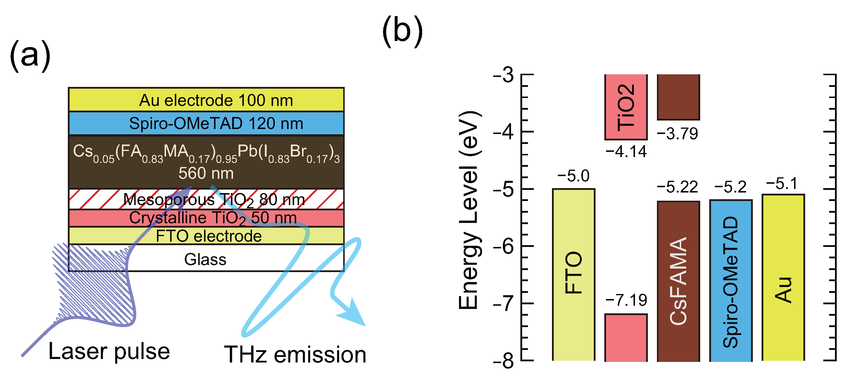
Figure 1a shows a schematic of the perovskite solar cell used in this experiment. The solar cell samples are glass-sealed perovskite solar cells, with an evaporated Au top electrode, a spin-coated 2,2’,7,7’-Tetrakis(N,N-di-p-methoxyphenylamino)-9,9’-spirobifluorene (Spiro-OMeTAD) hole transport layer, a Cs
(FA
MA
)
Pb(I
Br
)
active layer, a mesoporous TiO
and crystalline TiO
electron transport layer, and a fluorine-doped tin oxide (FTO) transparent electrode. This solar cell was built based on the study by Saliba et al. [
34].
Figure 1b shows the band diagram assumed for the sample solar cell. The energy levels of the frontier orbitals from the literature were used for each layer [
35,
36,
37,
38,
39,
40]. The values for the mesoporous titanium dioxide layer are not shown.
The LTEM consists of a Ti–sapphire pulse laser, a beam splitter, a second harmonic generator, a delay stage, an X–Y sample stage, a Hamamatsu Photonics G10620-13 low-temperature-grown GaAs photoconductive module with a spiral antenna, mirrors, and lock-in amps with PCs. An 800 nm pulsed light from the laser is separated by the beam splitter and one pulse is converted to a 400 nm wavelength pulse through the second harmonic generator, and then excites the sample. The THz radiation from the sample is focused on the GaAs sensor. The other 800 nm pulse illuminates the sensor after passing through a delay stage. The sensor generates photocurrent when the 800 nm pulse reaches the sensor. If the THz radiation from the perovskite solar cell reaches the sensor at the same time, the photocurrent changes according to the amplitude of the electric field of the THz radiation. The waveform of the THz radiation is measured by sweeping the delay stage while measuring the change of photocurrent using the lock-in amplifier. A detailed analysis of the waveforms of THz radiation is beyond the scope of this communication because, although the G10620-13 with spiral antenna exhibits high sensitivity, it is empirically known that its time response function significantly affects the observed waveforms.
The LTEM images in the subsequent sections were obtained from similar perovskite solar cells with a power conversion efficiency of 9.98%, 0.63%, and 0.00%. The second and third cells were stored at 85 °C and 85% relative humidity for 72 h before measurement. The I-V measurement for
Figure 2 was carried out using San-Ei Electric XHS-80S1 solar simulator and ADCMT 6241A DC voltage current source/monitor.
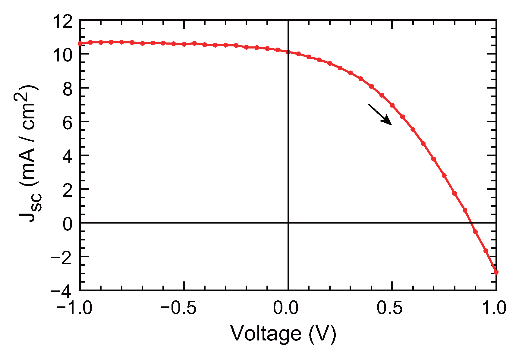
2. J-V Characteristics of the Sample Cell
Figure 2 shows the J-V characteristics of the sample cell at the time of the LTEM measurements in a solar simulator. The filled red circles show a two terminal voltage sweep from −1 V to 1 V, and the waiting time at each measurement point indicated by the circles is 400 ms. The filled red circles show a two-terminal voltage sweep from −1 V to 1 V. The J–V curve shows a J
of 10.1 mA/cm
2 of 0.88 V, and an energy conversion efficiency of 3.5%. The current did not significantly leak when this sample was reverse biased. Therefore, the sample is suitable for the measurement using LTEM in which light pulses irradiate the sample while reverse bias is applied. In the LTEM measurement, large reverse bias was applied, risking damage to the sample, but significant breakdown was not observed until applying −14 V.
3. Results: THz Waveforms and Reverse Bias Voltage
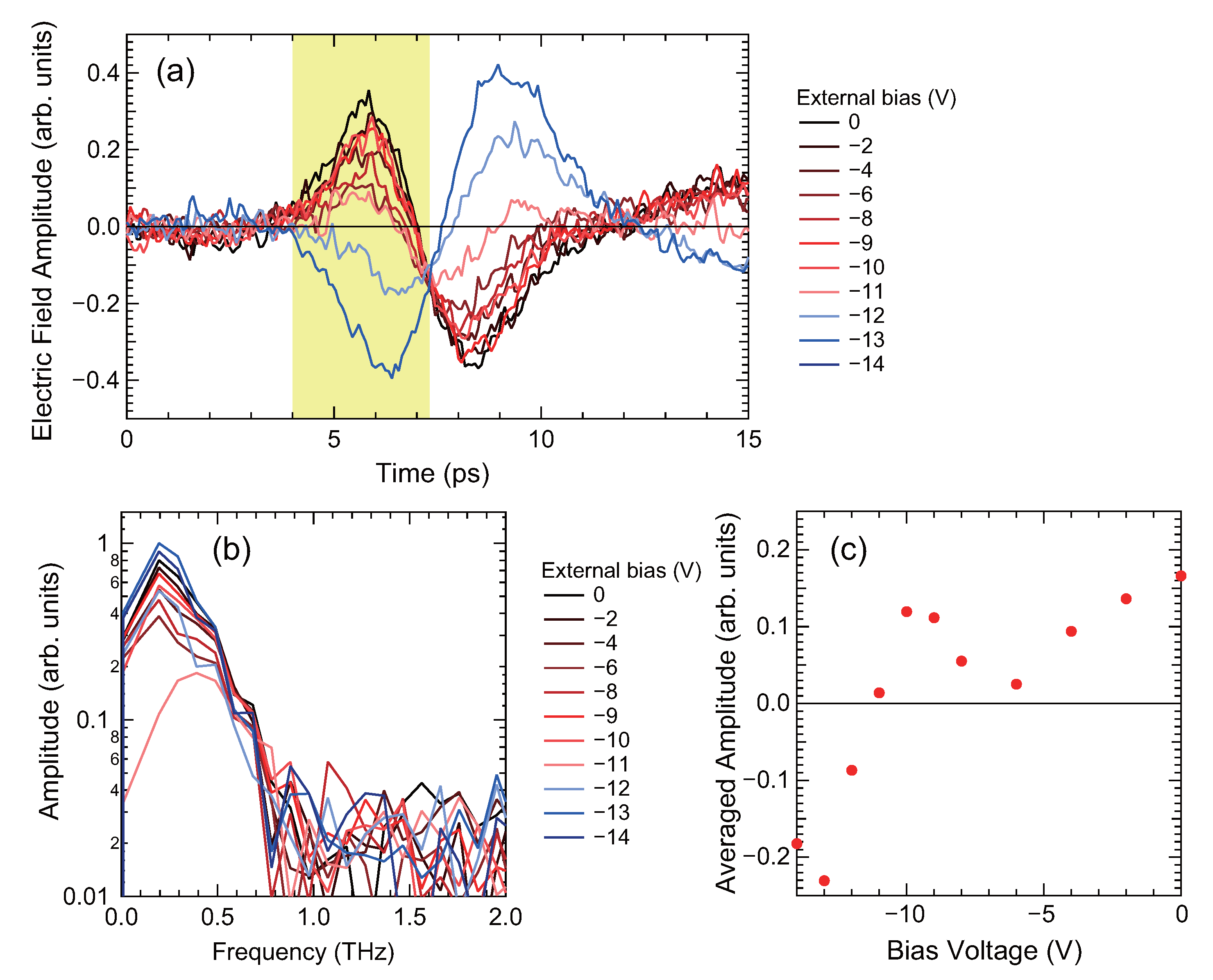
Figure 3a shows the waveform of a perovskite solar cell at various reverse bias voltages. Forward bias voltage was not applied because a large forward current would instantly destroy the sample. Reverse bias voltage above −15 V was not applied because significant breakdown was observed after the measurement at −14 V. The waveform of the THz radiation changes with the reverse bias voltage, and the waveform inverted above −12 V. The observed THz radiation waveform is strongly influenced by the transient response of the GaAs sensor. The first peaks shown in the yellow rectangle can be related to the separation of photoexcited carriers by the photo-Dember effect and the acceleration by the interfacial electric field. We cannot separate these two effects using the current analysis. The waveform is measured with the GaAs sensor with the spiral antenna and FFT amplitudes of the sample, as shown in
Figure 3b and the details of waveform, particularly the second peak, are expected to be strongly affected by time-response function of the sensor.
Figure 3c shows the bias voltage dependence of the averaged intensity of the first peak in
Figure 3a. The peak intensity decreases with reverse bias up to −6 V, then increases to −10 V. The averaged amplitude is near zero at −11 V. The waveform inverted above −12 V. Therefore, the waveform of the THz radiation is partially related to the electric field at the interface between the TiO
layer and perovskite layer. The reverse bias is an electric field that directs electrons from the perovskite layer to the TiO
layer. The dip of the THz amplitude observed under the −6 V reverse bias is possibly related to physically meaningful phenomena such as hole trapping but is unable to interpret because the data are deficient at present. The sample could have been partially damaged during the measurement, and further examination is required.
4. Discussion
The observed continuous change of waveform and inversion of the THz radiation with external biases is qualitatively similar to our previous work [
24] on silicon metal oxide semiconductor samples, where field emission is the dominant source of the laser pulse-induced THz radiation. Therefore, we hypothesize that the observed change of the waveform is related to the contribution of field emission and the change of the internal electric field caused by external biases. For semiconductors, the relationship between the electric field
of the THz radiation, the polarization inside the sample
, and the current
is as follows [
16]:
The samples in this experiment are either short-circuited or reverse-biased solar cell samples. Thus, a large portion of the photoexcited carriers travel out of the sample as current, and the right-hand term of the equation is treated as the transient current. The origin of THz radiation is classified into two types: the field emission and photo-Dember effect. The field emission refers to the transient current caused by the separation and acceleration of photo-excited electrons and holes by band bending near the interface of the perovskite layer. The photo-Dember effect is the transient current caused by the difference between the mobility or diffusion constants of electrons and holes. When the laser pulses excite the sample, photogenerated electrons and holes are localized near the interface and share the center of mass. Because electrons and holes diffuse away from the interface at different speeds, the centers of mass of the electrons and holes shift, creating an effective transient current. The relation between
,
, and
enables the evaluation of transient transport at the interfaces in semiconductor devices by assessing the THz radiation. The waveform of the THz radiation without external bias voltage did not significantly change when we irradiated the sample from the Spiro-OMeTAD side (not shown here); therefore, we assumed that the photo-Dember effect is the dominant source of THz radiation, as shown for lead-halide perovskite thin films in previous work [
14]. The contribution of carrier transfer from the perovskite layer to the TiO
layer is also considered insignificant.
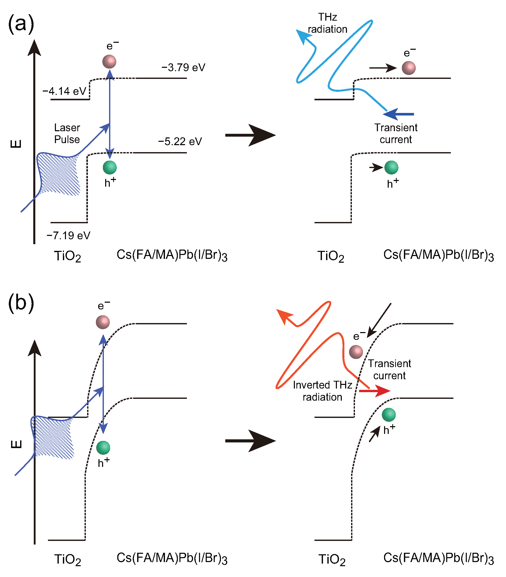
Figure 4 qualitatively illustrates the band diagram and carrier dynamics of a photoexcited electron and hole to explain the waveform inversion of the THz radiation with reverse bias voltage.
Figure 4a shows the band diagram and carrier dynamics in the absence of bias voltage. The dotted line shows the band bending near the interface between the TiO
and perovskite layers, assuming that the electron accumulated at the interface. We cannot accurately calculate the bending of the interface because the contribution of the trapped charge, fixed charge, and mesoporous layer at the interface [
41] is not known for our samples. Here, we assumed that a strong inversion layer is not formed, which impairs the characteristics of the solar cell. The electron mobility is higher than the hole and diffuses faster away from the interface. This causes a transient current normal to the interface, directed from the perovskite layer to the TiO
layer immediately after pulse excitation. The transient current generates the THz radiation. Assuming that the perovskite layer under measurement behaves as a doped semiconductor, and the TiO
layer behaves as an electrode, the externally applied reverse bias changes the interfacial electric field, as shown in
Figure 4b. Because the reverse bias of −12 V is larger than the interfacial voltage that can normally occur inside a solar cell, the band should bend significantly toward the TiO
interface regardless of the interfacial electric field without the bias. The interfacial electric field separates the photoexcited carriers, contributing to a transient current in the direction opposite to that of the photo-Dember effect. The interfacial electric field and photo-Dember effect destructively contributed to the formation of the transient current, and the net transient current inverted when the reverse bias voltage exceeded −12 V, causing an inversion of the waveform of the THz radiation. The inversion of the THz radiation waveform with an external bias voltage indicates that the interfacial electric field makes a significant contribution to the THz radiation from the solar cell sample. In addition, a large bias voltage for the inversion suggests that the photo-Dember effect is a dominant factor in the absence of external biases.
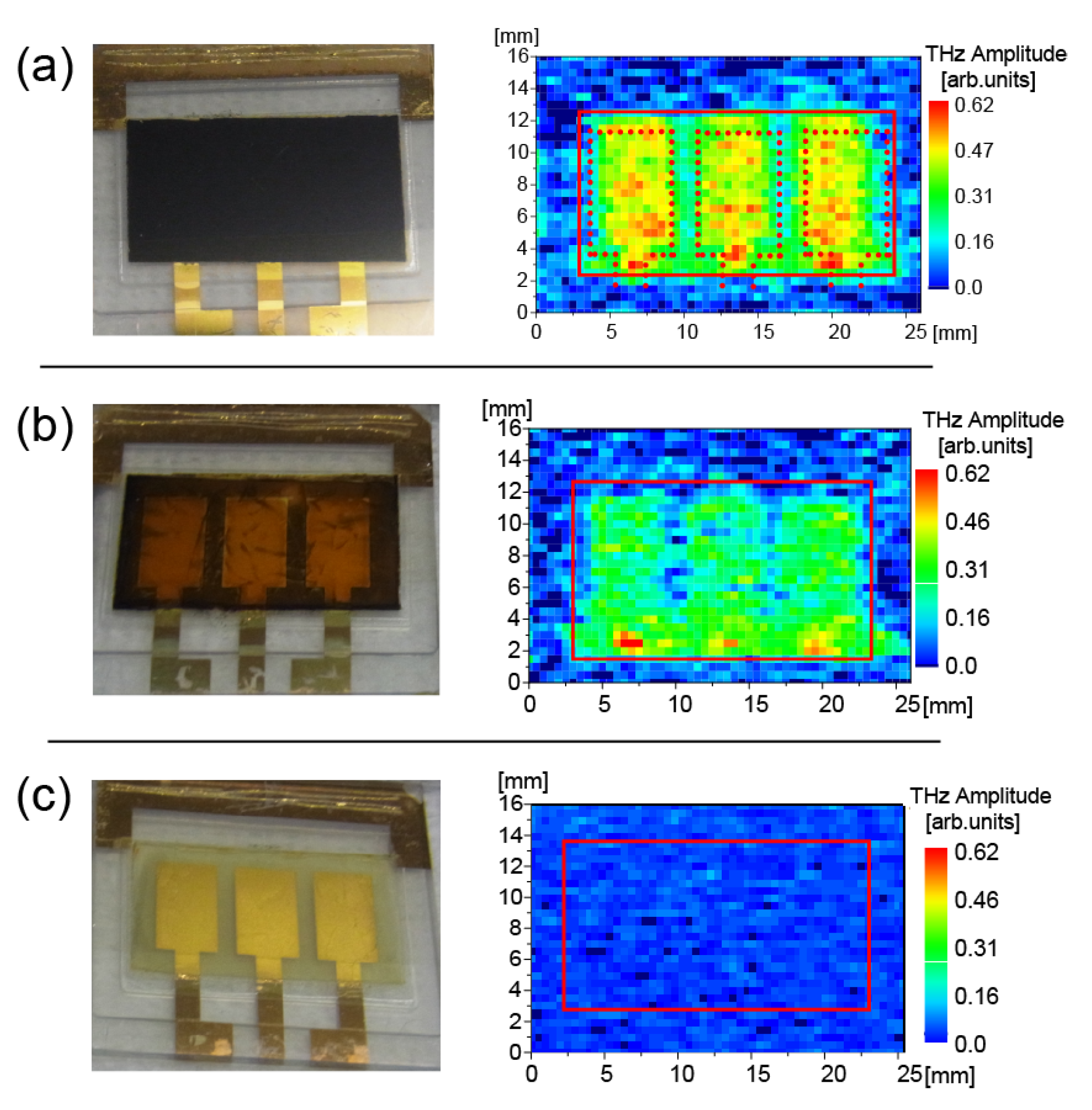
5. THz Radiation of the Degraded Cells
We measured the THz radiation of three perovskite cells with various degradation conditions to evaluate the changes in the electrical properties of the perovskite layers using LTEM. All samples have zero transmittance at the excitation wavelength of 400 nm.
Figure 5 shows the pictures and LTEM images of the solar cell samples. The LTEM images show the peak amplitude at 6 ps of THz radiation. The THz radiation was weaker in the degraded samples and undetectable in the sample with 0% efficiency. The images show that the absorption of the long-wavelength light is weakened by the decomposition of the perovskite layer in the degraded cells. The THz radiation amplitude is stronger for the Au electrodes shown in the red dots. Possibilities include the gold electrode acting as an antenna that enhanced THz radiation towards the GaAs sensor in LTEM by changing the shape of the escape cone of the THz radiation [
32], or it acting as a moisture proof film to suppress degradation. The detected signals which had the same sign as the sample shown in previous sections, suggesting that the THz radiation mainly originates from the photo-Dember effect. The smaller amplitude of the THz radiation from the degraded cell could be caused by the following factors: (1) decreased mobility near the interface resulting in a weaker transient current; or (2) an increased penetration length of the excitation light, causing the THz radiation to become insensitive to the interface.
6. Summary and Perspective
To summarize, we observed the THz radiation from the perovskite solar cells using LTEM. The waveform of the THz radiation changed with the applied reverse bias voltage, showing that the waveform was partly related to the internal electric field of the perovskite layer. The large reverse voltages required to invert the waveform are consistent with the lead-halide perovskite films where the photo-Dember effect is the dominant source of the transient current [
14]. The waveform inversion with the reverse bias also shows that the transient current was caused by the photo-Dember effect directed from the TiO
layer to the perovskite layer. More detailed knowledge on the carrier dynamics in perovskite solar cells related to physical quantities including electron number density, plasma frequency, complex conductivity, interface potentials, and fixed charge carrier density may be obtained by measuring with high-precision standard photoconductive antennas and the THz radiation changes based on various parameters, including excitation wavelength, intensity, and sample recipe, and analyzing them with a proper modeling of the THz radiation in future work.
Author Contributions
Conceptualization, T.M. and Y.Y.; methodology, T.M., Y.N., M.C., I.K. and M.T.; software, T.M.; validation, T.M., M.T., Y.Y. and H.T.; formal analysis, T.M.; investigation, T.M., I.K. and M.T.; resources, Y.N., M.C. and Y.Y.; data curation, T.M.; writing—original draft preparation, T.M.; writing—review and editing, M.T., Y.Y. and H.T.; visualization, T.M.; supervision, M.T., Y.Y. and H.T.; project administration, H.T.; funding acquisition, T.M. and H.T. All authors have read and agreed to the published version of the manuscript.
Funding
This work is partly supported by the New Energy and Industrial Technology Development Organization (NEDO), Japan, KAKENHI 20K05697, and The Iwatani Naoji Foundation.
Institutional Review Board Statement
Not applicable.
Informed Consent Statement
Not applicable.
Data Availability Statement
The data that support the findings of this study are available from the corresponding author, T.M., upon reasonable request.
Acknowledgments
We acknowledge technical support and discussions from Akira Ito and Hidetoshi Nakanishi of SCREEN Holdings Co., Ltd.
Conflicts of Interest
The authors declare no conflict of interest.
References
- Green, M.; Dunlop, E.; Hohl-Ebinger, J.; Yoshita, M.; Kopidakis, N.; Hao, X. Solar cell efficiency tables (version 57). Prog. Photovoltaics Res. Appl. 2021, 29, 3–15. [Google Scholar] [CrossRef]
- Patidar, R.; Burkitt, D.; Hooper, K.; Richards, D.; Watson, T. Slot-die coating of perovskite solar cells: An overview. Mater. Today Commun. 2020, 22, 100808. [Google Scholar] [CrossRef]
- Jeong, D.N.; Lee, D.K.; Seo, S.; Lim, S.Y.; Zhang, Y.; Shin, H.; Cheong, H.; Park, N.G. Perovskite Cluster-Containing Solution for Scalable D-Bar Coating toward High-Throughput Perovskite Solar Cells. ACS Energy Lett. 2019, 4, 1189–1195. [Google Scholar] [CrossRef]
- Wang, R.; Mujahid, M.; Duan, Y.; Wang, Z.; Xue, J.; Yang, Y. A Review of Perovskites Solar Cell Stability. Adv. Funct. Mater. 2019, 29, 1808843. [Google Scholar] [CrossRef]
- Hamukwaya, S.L.; Hao, H.; Zhao, Z.; Dong, J.; Zhong, T.; Xing, J.; Hao, L.; Mashingaidze, M.M. A Review of Recent Developments in Preparation Methods for Large-Area Perovskite Solar Cells. Coatings 2022, 12, 252. [Google Scholar] [CrossRef]
- Kojima, A.; Teshima, K.; Shirai, Y.; Miyasaka, T. Organometal Halide Perovskites as Visible-Light Sensitizers for Photovoltaic Cells. J. Am. Chem. Soc. 2009, 131, 6050–6051. [Google Scholar] [CrossRef]
- Yang, D.; Sano, T.; Yaguchi, Y.; Sun, H.; Sasabe, H.; Kido, J. Perovskite Solar Cells: Achieving 20% Efficiency for Low-Temperature-Processed Inverted Perovskite Solar Cells (Adv. Funct. Mater. 12/2019). Adv. Funct. Mater. 2019, 29, 1970074. [Google Scholar] [CrossRef] [Green Version]
- Osman, B.; Abdolkader, T.; Ahmed, I. A Review of Perovskite Solar Cells. Int. J. Mater. Technol. Innov. 2021, 1, 48–66. [Google Scholar] [CrossRef]
- Roose, B.; Wang, Q.; Abate, A. The Role of Charge Selective Contacts in Perovskite Solar Cell Stability. Adv. Energy Mater. 2018, 9, 1803140. [Google Scholar] [CrossRef]
- Jain, S.C.; Radhakrishna, S. Physics of Semiconductor Devices; World Scientific: Singapore, 1987; pp. 1–546. [Google Scholar] [CrossRef]
- Barnea-Nehoshtan, L.; Kirmayer, S.; Edri, E.; Hodes, G.; Cahen, D. Surface Photovoltage Spectroscopy Study of Organo-Lead Perovskite Solar Cells. J. Phys. Chem. Lett. 2014, 5, 2408–2413. [Google Scholar] [CrossRef]
- Schulz, P.; Edri, E.; Kirmayer, S.; Hodes, G.; Cahen, D.; Kahn, A. Interface energetics in organo-metal halide perovskite-based photovoltaic cells. Energy Environ. Sci. 2014, 7, 1377. [Google Scholar] [CrossRef]
- Obraztsov, P.A.; Lyashenko, D.; Chizhov, P.A.; Konishi, K.; Nemoto, N.; Kuwata-Gonokami, M.; Welch, E.; Obraztsov, A.N.; Zakhidov, A. Ultrafast zero-bias photocurrent and terahertz emission in hybrid perovskites. Commun. Phys. 2018, 1, 14. [Google Scholar] [CrossRef] [Green Version]
- Guzelturk, B.; Belisle, R.A.; Smith, M.D.; Bruening, K.; Prasanna, R.; Yuan, Y.; Gopalan, V.; Tassone, C.J.; Karunadasa, H.I.; McGehee, M.D.; et al. Terahertz Emission from Hybrid Perovskites Driven by Ultrafast Charge Separation and Strong Electron–Phonon Coupling. Adv. Mater. 2018, 30, 1704737. [Google Scholar] [CrossRef] [PubMed]
- Rana, D.S.; Tonouchi, M. Terahertz Emission Functionality of High-Temperature Superconductors and Similar Complex Systems. Adv. Opt. Mater. 2020, 8, 1900892. [Google Scholar] [CrossRef]
- Tonouchi, M. Cutting-edge terahertz technology. Nat. Photonics 2007, 1, 97–105. [Google Scholar] [CrossRef]
- Nakanishi, H.; Fujiwara, S.; Takayama, K.; Kawayama, I.; Murakami, H.; Tonouchi, M. Imaging of a Polycrystalline Silicon Solar Cell Using a Laser Terahertz Emission Microscope. Appl. Phys. Express 2012, 5, 112301. [Google Scholar] [CrossRef]
- Murakami, H.; Serita, K.; Maekawa, Y.; Fujiwara, S.; Matsuda, E.; Kim, S.; Kawayama, I.; Tonouchi, M. Scanning laser THz imaging system. J. Phys. D Appl. Phys. 2014, 47, 374007. [Google Scholar] [CrossRef]
- Nakanishi, H.; Ito, A.; Takayama, K.; Kawayama, I.; Murakami, H.; Tonouchi, M. Comparison between laser terahertz emission microscope and conventional methods for analysis of polycrystalline silicon solar cell. AIP Adv. 2015, 5, 117129. [Google Scholar] [CrossRef]
- Murakami, H.; Fujiwara, S.; Kawayama, I.; Tonouchi, M. Study of photoexcited-carrier dynamics in GaAs photoconductive switches using dynamic terahertz emission microscopy. Photonics Res. 2016, 4, A9. [Google Scholar] [CrossRef]
- Sakai, Y.; Kawayama, I.; Nakanishi, H.; Tonouchi, M. Polarization imaging of imperfect m-plane GaN surfaces. APL Photonics 2017, 2, 041304. [Google Scholar] [CrossRef] [Green Version]
- Hotta, Y.; Kawayama, I.; Miyake, S.; Saiki, I.; Nishi, S.; Yamahara, K.; Arafune, K.; Yoshida, H.; Satoh, S.I.; Sawamoto, N.; et al. Control of dipole properties in high-k and SiO2 stacks on Si substrates with tricolor superstructure. Appl. Phys. Lett. 2018, 113, 012103. [Google Scholar] [CrossRef]
- Mochizuki, T.; Ito, A.; Mitchell, J.; Nakanishi, H.; Tanahashi, K.; Kawayama, I.; Tonouchi, M.; Shirasawa, K.; Takato, H. Probing the surface potential of oxidized silicon by assessing terahertz emission. Appl. Phys. Lett. 2017, 110, 163502. [Google Scholar] [CrossRef]
- Mochizuki, T.; Ito, A.; Nakanishi, H.; Tanahashi, K.; Kawayama, I.; Tonouchi, M.; Shirasawa, K.; Takato, H. Noncontact evaluation of electrical passivation of oxidized silicon using laser terahertz emission microscope and corona charging. J. Appl. Phys. 2019, 125, 151615. [Google Scholar] [CrossRef]
- Baranowski, M.; Plochocka, P. Excitons in Metal-Halide Perovskites. Adv. Energy Mater. 2020, 10, 1903659. [Google Scholar] [CrossRef]
- Zhang, X.; Hu, B.B.; Darrow, J.T.; Auston, D.H. Generation of femtosecond electromagnetic pulses from semiconductor surfaces. Appl. Phys. Lett. 1990, 56, 1011–1013. [Google Scholar] [CrossRef]
- Zhang, X.; Auston, D.H. Optoelectronic measurement of semiconductor surfaces and interfaces with femtosecond optics. J. Appl. Phys. 1992, 71, 326–338. [Google Scholar] [CrossRef]
- Ulbricht, R.; Hendry, E.; Shan, J.; Heinz, T.F.; Bonn, M. Carrier dynamics in semiconductors studied with time-resolved terahertz spectroscopy. Rev. Mod. Phys. 2011, 83, 543–586. [Google Scholar] [CrossRef] [Green Version]
- Hoyer, P.; Theuer, M.; Beigang, R.; Kley, E.B. Terahertz emission from black silicon. Appl. Phys. Lett. 2008, 93, 091106. [Google Scholar] [CrossRef]
- Blumröder, U.; Steglich, M.; Schrempel, F.; Hoyer, P.; Nolte, S. THz emission from argon implanted silicon surfaces. Phys. Status Solidi 2015, 252, 105–111. [Google Scholar] [CrossRef]
- Sher, M.J.; Simmons, C.B.; Krich, J.J.; Akey, A.J.; Winkler, M.T.; Recht, D.; Buonassisi, T.; Aziz, M.J.; Lindenberg, A.M. Picosecond carrier recombination dynamics in chalcogen-hyperdoped silicon. Appl. Phys. Lett. 2014, 105, 053905. [Google Scholar] [CrossRef] [Green Version]
- Johnston, M.B.; Whittaker, D.M.; Corchia, A.; Davies, A.G.; Linfield, E.H. Simulation of terahertz generation at semiconductor surfaces. Phys. Rev. B 2002, 65, 165301. [Google Scholar] [CrossRef] [Green Version]
- Bereznaya, S.; Korotchenko, Z.; Redkin, R.; Sarkisov, S.; Brudnyi, V.; Kosobutsky, A.; Atuchin, V. Terahertz generation from electron- and neutron-irradiated semiconductor crystal surfaces. Infrared Phys. Technol. 2016, 77, 100–103. [Google Scholar] [CrossRef]
- Saliba, M.; Matsui, T.; Seo, J.Y.; Domanski, K.; Correa-Baena, J.P.; Nazeeruddin, M.K.; Zakeeruddin, S.M.; Tress, W.; Abate, A.; Hagfeldt, A.; et al. Cesium-containing triple cation perovskite solar cells: Improved stability, reproducibility and high efficiency. Energy Environ. Sci. 2016, 9, 1989–1997. [Google Scholar] [CrossRef] [PubMed] [Green Version]
- Helander, M.G.; Greiner, M.T.; Wang, Z.B.; Tang, W.M.; Lu, Z.H. Work function of fluorine doped tin oxide. J. Vac. Sci. Technol. A Vacuum Surfaces Film. 2011, 29, 011019. [Google Scholar] [CrossRef]
- Nowotny, J. Oxide Semiconductors for Solar Energy Conversion; CRC Press: Boca Raton, FL, USA, 2016. [Google Scholar] [CrossRef]
- Mansfeldova, V.; Zlamalova, M.; Tarabkova, H.; Janda, P.; Vorokhta, M.; Piliai, L.; Kavan, L. Work Function of TiO2 (Anatase, Rutile, and Brookite) Single Crystals: Effects of the Environment. J. Phys. Chem. C 2021, 125, 1902–1912. [Google Scholar] [CrossRef]
- Wang, Q.; Mosconi, E.; Wolff, C.; Li, J.; Neher, D.; De Angelis, F.; Suranna, G.P.; Grisorio, R.; Abate, A. Rationalizing the Molecular Design of Hole-Selective Contacts to Improve Charge Extraction in Perovskite Solar Cells. Adv. Energy Mater. 2019, 9, 1900990. [Google Scholar] [CrossRef]
- Li, Y.; Li, H.; Zhong, C.; Sini, G.; Brédas, J.L. Characterization of intrinsic hole transport in single-crystal spiro-OMeTAD. Npj Flex. Electron. 2017, 1, 2. [Google Scholar] [CrossRef] [Green Version]
- Sachtler, W.; Dorgelo, G.; Holscher, A. The work function of gold. Surf. Sci. 1966, 5, 221–229. [Google Scholar] [CrossRef]
- Niu, B.; Wang, X.; Wu, K.; He, X.; Zhang, R. Mesoporous Titanium Dioxide: Synthesis and Applications in Photocatalysis, Energy and Biology. Materials 2018, 11, 1910. [Google Scholar] [CrossRef] [Green Version]
| Publisher’s Note: MDPI stays neutral with regard to jurisdictional claims in published maps and institutional affiliations. |
© 2022 by the authors. Licensee MDPI, Basel, Switzerland. This article is an open access article distributed under the terms and conditions of the Creative Commons Attribution (CC BY) license (https://creativecommons.org/licenses/by/4.0/).

 ,
, 


