Abstract
We proposed an ultra-sensitive refractive index sensor by using indium-doped cadmium oxide as a plasmonic material operating in near-infrared based on Fano resonance. The proposed sensor has a hybrid multilayer waveguide structure that supports both a long-range surface plasmon polariton (LRSPP) mode and a dielectric waveguide (DWG) mode. The design strategy of the structure parameters of the inner layers is elaborated in detail through the numerical analysis of the two modes. By suitably tailoring the thickness of the coupling layer, a strong mode coupling between the two modes could be achieved, leading to a sharp asymmetric Fano resonance. With the designed optimal physical parameters, our proposed sensor could achieve a maximum intensity sensitivity of 19,909 RIU−1, a 193-fold enhancement than that of a conventional long-range SPR (LRSPR) based scheme. The proposed design can be a promising platform for biochemical sensing in the near-infrared region.
1. Introduction
The surface plasmon resonance (SPR) technique has been successfully proven to advance the development of high-performance sensing optical devices due to the unique features of rapid, real-time, noninvasive, label-free, and level-free detection. However, the broad resonance dip produced by conventional SPR techniques based on Otto [1] and Kretschmann [2] configurations limits the sensitivity and resolution. Various approaches with a four-layer structure such as bimetallic approaches [3,4], guided-wave SPR [5,6], and long-range SPR (LRSPR) [7,8] based on long-range SPP (LRSPP) mode [9,10] have been explored to produce a sharp resonance dip to improve sensing resolutions. This is because the electric field strength at the sensing surface of the 4-layer based sensors [3,4,5,6,7,8] can be greatly enhanced, making them more sensitive to the refractive index change of the sensing analyte. Consequently, a resonance curve with a much narrower full width at half maximum (FWHM) could be achieved, resulting in a significant enhancement in sensitivity compared to the conventional SPR sensors [1,2].
In recent years, there have been continuous efforts to further improve the sensitivity of SPR based sensors by using hybrid multilayer plasmonic platforms formed by a combination of plasmonic and photonic structures [11,12]. Wu et al. [11] and Li et al. [12] proposed hybrid 6-layer configurations composed of the LRSPP mode and dielectric waveguide (DWG) mode to produce two narrow resonance dips, achieving maximum sensitivities of 3619 RIU−1 and 3081 RIU−1, respectively. With a 5-layer hybrid plasmonic platform, ultrahigh-resolution sensors based on the strong mode coupling between the conventional SPP mode and DWG mode (serving as broad and dark modes) have been presented [13,14,15,16,17,18]. Due to the interference of the two modes, Fano resonance and plasmonic-induced transparency (PIT) could be realized. Alternatively, Fano resonances have been achieved in double waveguides with the help of 2D nanomaterials, such as graphene [19] and molybdenum disulfide (MoS2) [20], as absorbers to generate a broad mode. Fano resonance can also be realized in different systems, such as plasmonic coupled waveguide-cavity systems [21,22], photonic crystals [23], metamaterials [24], and plasmonic nanostructures [25]. Unlike the conventional resonance with a symmetric Lorentzian lineshape, Fano resonance exhibits an asymmetric lineshape with extremely narrow linewidth. Fano resonance has attracted extensive research for various applications [26,27,28,29,30,31] in developing optical switches, sensors, and filters with enhanced optical performances.
SPR-based sensors mentioned above are focused in the visible wavelength range using noble metal for plasmonic structures. The research progress on plasmonics applied in the infrared spectral region is opening new opportunities [32,33] in infrared sources, detectors, switches, modulators, and sensors. Recently, SPR-based sensors operating in the infrared regime have attracted considerable interest due to their potential applications in biomedicine, biochemistry, environmental monitoring, etc. However, noble metals such as gold, silver, and aluminum, are not appropriate plasmonic conductors for the infrared region due to dramatically increased optical loss in the infrared regime. On the other hand, transparent conductive oxide (TCO) materials [34,35,36] have been recently found to have potential near- and mid-infrared plasmonic applications in chemical sensing, thermal imaging, heat harvesting, and infrared detectors. In contrast to commonly adopted noble metals, TCOs could have relatively high and adjustable charge carrier densities by using different approaches, such as heavily doping, electrical gating, and inter- or intraband optical excitation, which makes them excellent gateway plasmonic materials to extend the SPR phenomenon from the visible to the infrared range. For example, Ruan et al. [37] proposed an LRSPR-based biosensor by using Ga-doped zinc oxide (GZO), which operates at 1550 nm. By adding a graphene layer between GZO and the sensing region layer, Pal et al. [38] improved the sensitivity of the biosensor from 150 RIU−1 to 367 RIU−1. Pal et al. [39] further proposed an LRSPR-based sensor with Al-doped zinc oxide (AZO) for plasmon generation and achieved a maximum sensitivity of 426 RIU−1. However, the sensitivities of these sensors are still limited. To further improve the performances of the TCO-based biosensors in the near-infrared region, a five-layer waveguide-coupled Fano resonance-enhanced SPR system [40] was proposed by Huang et al. using indium tin oxide (ITO), serving as the plasmonic material, where a maximum sensitivity of 104 RIU−1 was achieved. Among TCOs, cadmium oxide (CdO) has high free charge mobility, enabling it to have a narrow SPR spectrum. Dysprosium-doped CdO and fluorine-doped cadmium oxide CdOs were reported for conventional SPRs in the Kretschman configuration [41,42]. Yang et al. [43] recently demonstrated optical polarization switching by using high-mobility indium-doped CdO as a perfect absorber.
In this paper, an ultra-sensitive refractive index sensor is proposed using indium-doped CdO as plasmonic material operating in near-infrared based on Fano resonance. The proposed structure consists of six layers formed by Prism/Teflon/CdO/Teflon/Si/Analyte. The thicknesses of the inner four layers play an important role in the excitation and the coupling of the DWG mode and LRSPP mode, which have been investigated in detail. Fano resonance, arisen from the strong coupling of the two modes, has been verified by the electric field distribution at the resonance angles, accompanied with the attenuated total reflection (ATR) curves. By suitably tailoring the thickness of the coupling layer, the asymmetric Fano resonance and PIT could be realized. A maximum intensity sensitivity of 19,909 RIU−1 was achieved with the optimized design. The proposed CdO-based six-layer hybrid plasmonic sensor could be a promising candidate for near-infrared sensing applications that require high-performance RI sensing.
2. Theoretical Model and Analysis Methods
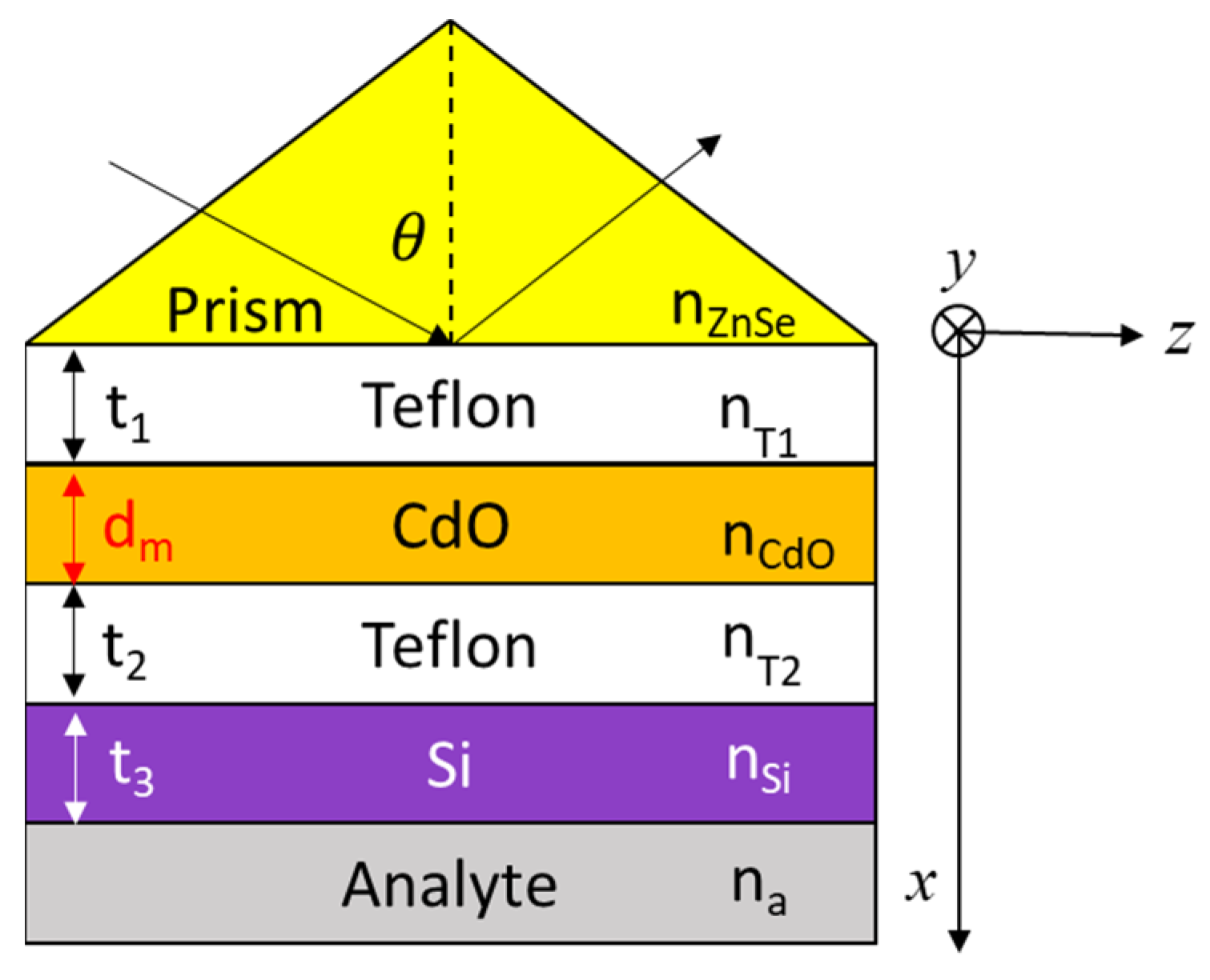
Figure 1 shows a cross-section view of the proposed multilayer hybrid biosensor in the z-x plane. It has six layers (including the prism layer), which are comprised of a Zinc Selenide (ZnSe) prism, Teflon AF1300, indium-doped Cadmium Oxide (CdO), Teflon AF1300, Silicon (Si), and the sensing analyte. The physical parameters are the material thicknesses of the inner layers that are denoted by t1, dm, t2, t3 for layer 2 to layer 5, respectively. For the proposed scheme, when a p-polarized light is incident upon the prism with the satisfied momentum-matching condition, an LRSPP mode could be excited, supported by the four-layer asymmetric structure (ZnSeprism/Teflon/CdO/Teflon). With a suitable thickness t2 of the coupling Teflon layer (layer 4), the evanescent field of LRSPP mode in the coupling Teflon region penetrates to the adjacent DWG structure (Teflon/Si/Analyte), which excites the DWG mode with a relatively narrow resonance spectrum. Due to the strong field coupling between the two different modes, Fano resonance can be realized where the LRSPP mode and DWG mode serve as bright and dark modes, respectively.

Figure 1.
Schematic diagram of a hybrid waveguide-coupled CdO-based plasmonic sensor.
The wavelength-dependent effective refractive index of the ZnSe prism, Teflon AF1300, and Si materials was calculated by the standard Sellmeier equation given by:
where n is the refractive index, λ is the operational wavelength, Bi and Ci are the experimentally derived Sellmeier coefficients [44,45,46,47], which are provided in Table 1 for the three materials.

Table 1.
The experimentally derived Sellmeier coefficients for ZnSe, Teflon, and Si.
According to the Drude model [43], the dielectric constant of transparent conductor CdO can be expressed by:
with the plasma frequency ωp given by:
where ε∞ is the high-frequency dielectric constant, ω is the angular frequency of the light wave, γ is the damping degree, n is the electron density, e is the electron charge, meff is the effective mass of the electron, and ε0 is the vacuum absolute permittivity. The values of ε∞, γ, n, e, meff and ε0 used in this work are 5.5, rad/s, m−3, C, kg, and F/m, respectively [48]. The complex relative permittivity of CdO is calculated by using Equations (2) and (3). Figure 2 shows the real part and imaginary part of the permittivity varies with wavelength. For wavelengths larger (smaller) than 1510 nm, the real part of the permittivity is negative (positive) with a relatively small value of the imaginary part, which makes it a functional material able to support the SPP (DWG) mode in the near-infrared regime.
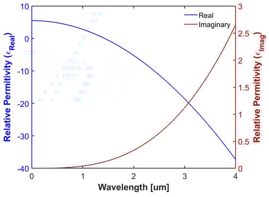
Figure 2.
The relative permittivity of CdO.
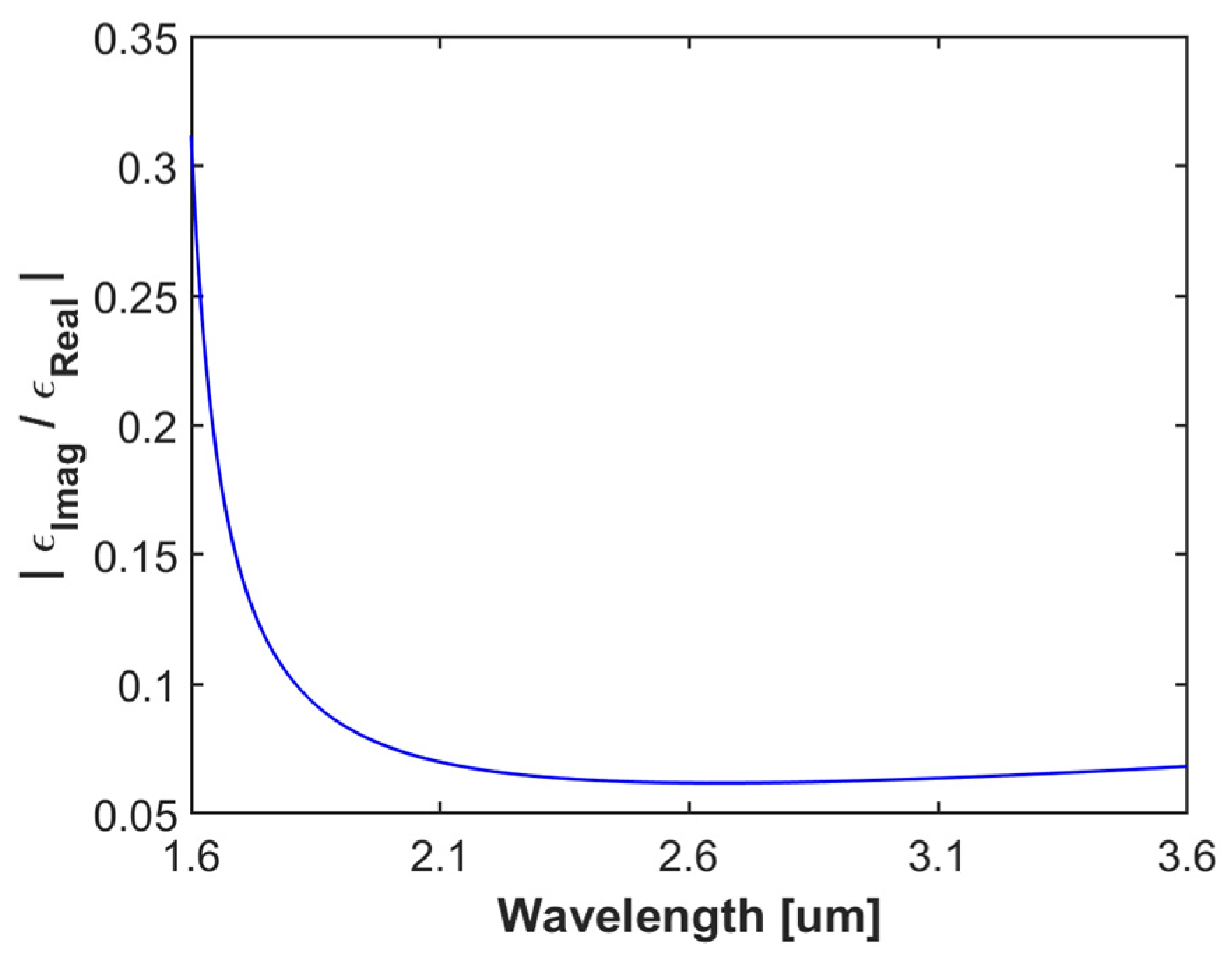
It is known that the permittivity of the plasmonic material has a significant impact on the performance of the SPR sensors. For example, the enhanced evanescent field could be obtained with a large value of |εReal|, giving rise to a sharp ATR curve. On the other hand, the imaginary component is a damping factor, and a large εImag would broaden the ATR curve. As a result, a smaller permittivity component ratio |εImag/εReal| is highly desirable for improving sensitivity. To determine the optimized operating wavelength for the proposed sensor, we calculated the permittivity component ratio |εImag/εReal| of CdO in terms of wavelength, as shown in Figure 3. It can be seen in Figure 3 that with increasing wavelength, the permittivity component ratio decreases in the near-infrared region with a minimum ratio at 2.66 μm and slightly increases in the mid-infrared region. For applications, considering the near-infrared Tm-doped laser source available on the market [49], the optimized operating wavelength was set to 1890 nm.
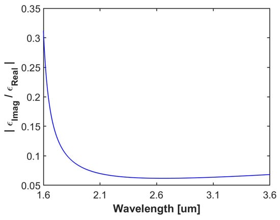
Figure 3.
Permittivity component ratio |εImag/εReal| of CdO as a function of the wavelength.
To obtain the reflectance of the proposed hybrid multilayer structure, the general N-layer model [50] was employed by using the transfer matrix method [51] with N corresponding to the number of layers in the waveguide. There are six layers in our configuration, i.e., N = 6, i.e., two outer layers (i = 1 for the prism and i = 6 for the analyte layer) and four inner layers. The individual transfer matrix for the inner layers (i = 2 to N − 1) is given by:
where
and
εi and di are the corresponding permittivity and thickness of the ith layer. λ is the operating wavelength, n1 is the refractive index of the prism, and θ1 is the incident angle at which the p-polarized light enters the sensor system. The characteristic transfer matrix M for the combined inner layers is written as:
The amplitude reflection coefficient rp can be expressed for the p-polarized incident light as:
where q1 and qN for the outer prism and analyte layer can be calculated from Equation (6). Thus, the reflectance Rp of the proposed multilayer system for p-polarized light could be calculated by:
To evaluate the performance of our SPR based sensor system, the sensitivity and quality factor (Q-factor) were calculated. In general, sensitivity can be determined by angular modulation [52] or by the intensity modulation method [19]. In our case, we leverage the sensing by intensity modulation method to evaluate the performance of the proposed sensor. This method measures the change in reflectance caused by the change in the sensing medium’s refractive index, and it is expressed by:
where ∆n is the change in the refractive index of the sensing medium and ∆R corresponds to the change in the reflectivity for a given incident angle θ. Note that the maximum SIntensity is often referred to as peak sensitivity [11,12] or the figure of merit (FOM) [18,19]. On the other hand, the Q-factor is the measure of the sharpness and intensity of the resonance caused by a change in a specific layer in the multilayer system, often used in Fano resonance. The Q-factor is defined as
where θ corresponds to the resonance angle of Fano resonance and ∆θ is the difference between the reflection peak and the reflection dip. Although Q does not correspond to the sensitivity of the plasmonic sensors in any way, it helps to achieve a narrow resonance without losing signal sharpness [53].
3. Numerical Results and Discussion
As mentioned in Section 2, the proposed hybrid 6-layer plasmonic sensor is based on Fano resonance, which comes from the mode coupling of the DWG and LRSPP modes. We first begin with the investigation of the DWG mode (formed by 3-layer Teflon/Si/Analyte structure) and the LRSPP mode (formed by 3-layer Teflon/CdO/Teflon structure). Then, we study the LRSPP mode of the 4-layer asymmetric structure (formed by Prism/Teflon/CdO/Teflon), followed by the strategy of combining the 3-layer dielectric waveguide and 4-layer asymmetric plasmonic waveguide to form a hybrid 6-layer plasmonic structure for achieving Fano resonance. For the proposed sensing system, water is used as the sensing analyte, and its refractive index is 1.309 at the operating wavelength of 1.89 μm [54]. By using Equations (1)–(3) and the constants in Table 1, we can find the refractive indices of the prism, Teflon, and silicon, as well as the permittivity of CdO, which are 2.448, 1.297, 3.457, and [−2.838 + 0.244i], respectively.
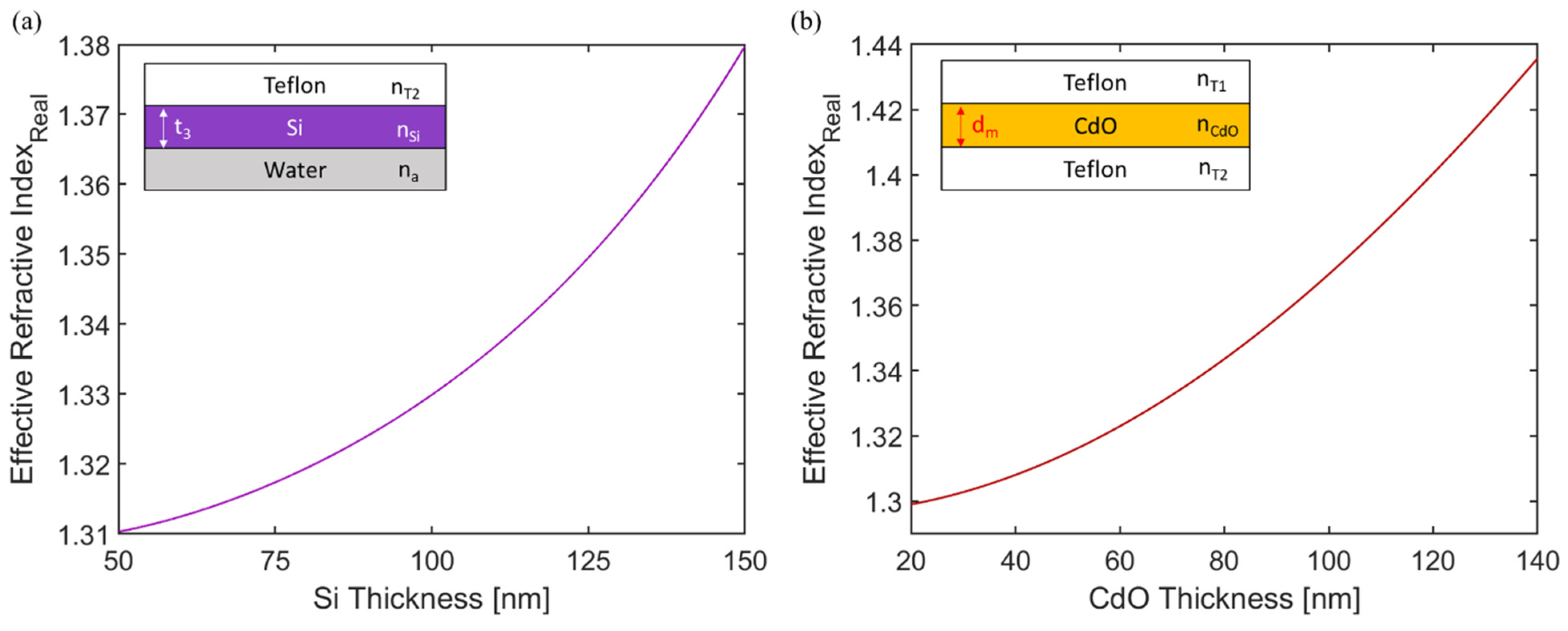
Figure 4a shows the calculated modal index of the 3-layer asymmetric Teflon/Si/Water DWG structure, which increases with increasing the thickness of the center high-index layer Si. The calculated modal index of the symmetric 3-layer Teflon/CdO/Teflon plasmonic structure is displayed in Figure 4b. The modal index of the LRSPP mode spans from 1.3 to 1.44 for the range of the CdO thickness from 20 nm to 140 nm. In order to effectively couple the DWG mode with the LRSPP mode, the modal indices of the two modes have to be in the close vicinity of each other and also slightly higher than the refractive index of the sensing analyte. Thus, the thicknesses of Si and CdO were chosen to be 66 nm and 62 nm, respectively.
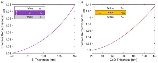
Figure 4.
Modal indices of (a) the 3-layer Teflon/Si/Water DWG structure and (b) the 3-layer Teflon/CdO/Teflon plasmonic structure.
Next, on top of the 3-layer Teflon/CdO/Teflon plasmonic structure, we added the ZnSe prism layer to form a 4-layer asymmetric plasmonic waveguide structure (see Figure 5 insert) for the excitation of the LRSPP mode. We calculated the modal index of the 4-layer structure and the reflectance at the resonance angle for different Teflon (2nd layer) thickness t1 with a fixed CdO thickness at 62 μm, as shown in Figure 5. With increasing t1, the modal index increases, corresponding to an increase in the resonance angle at the ATR curve. Note that the reflectance at the resonance angle is the smallest value at the resonance dip. From Figure 5, it is obvious that the optimum thickness of the Teflon layer t1 is around 1.84 μm, where the minimum reflectance Rmin at the resonance angle reaches zero.
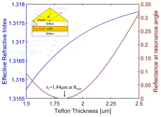
Figure 5.
Modal index and reflectance at the resonance angle as a function of the Teflon thicknesses t1.
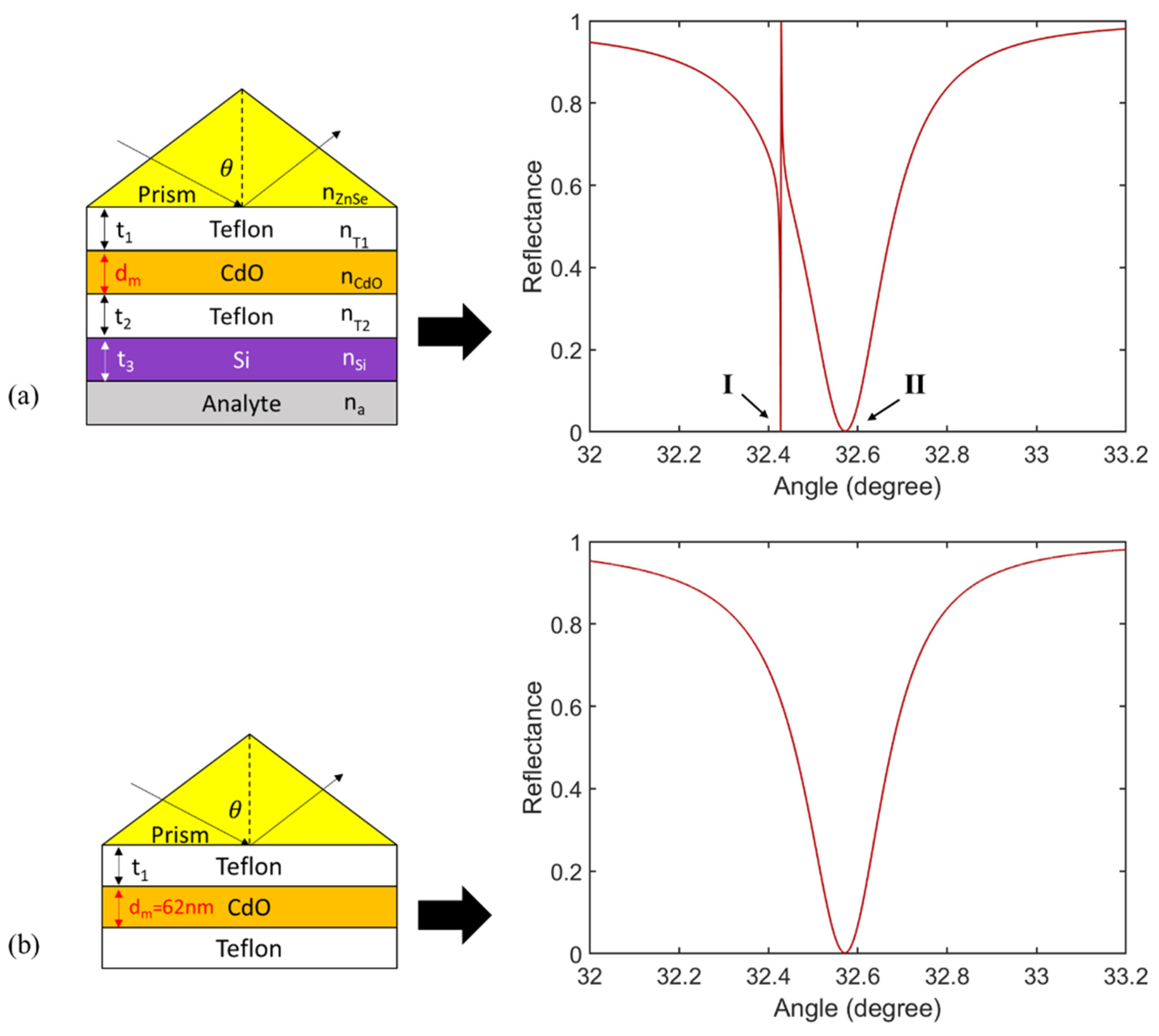
By integrating the 4-layer plasmonic waveguide with the 3-layer DWG, a six-layer CdO-based hybrid waveguide-coupled plasmonic structure (as shown in the left Figure 6a) was proposed for ultrasensitive sensing in the near-infrared range. Per the previous discussion, the thicknesses of the inner four layers were designed to be t1 = 1.84 μm, dm = 62 nm, and t3 = 66 nm, where the 4th-layer thickness was chosen to be t2 = 5.475 μm. The reflection spectrum of the proposed sensor is displayed on the right-hand side of Figure 6a. In the configuration, the 4th layer (Teflon) serves as the coupling layer. With a suitable thickness t2 of the 4th layer, the evanescent field excited from the LRSPP mode at the coupling layer penetrates into the DWG structure and excites the DWG mode, giving rise to a sharp Fano resonance. From the ATR curve in Figure 6a, one can clearly see the Fano resonance with a distinctly asymmetric dip at point I as the dark mode on the left wing of the relatively broad dip at point II as the bright mode. The sharp resonance and broad resonance occur at the incident angle of 32.4275° and 32.5717° respectively, attributed to the excitation of the DWG mode and LRSPP mode, with a corresponding modal index of 1.3126 and 1.3178, respectively. For comparison, we also plotted the ATR curve in Figure 6b for a 4-layer plasmonic structure (see the left of Figure 6b) with the absence of the DWG layers, which shows the excitation of the LRSPP mode only.
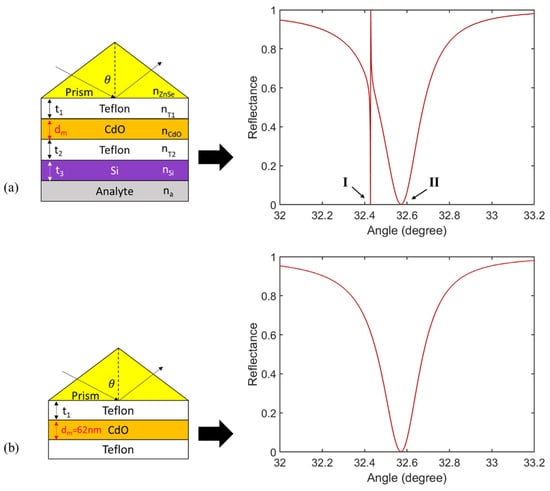
Figure 6.
Schematic diagram and the corresponding reflection spectra of (a) the proposed 6-layer Fano resonance structure at λ = 1.89 μm and (b) the 4-layer LRSPR structure for comparison.
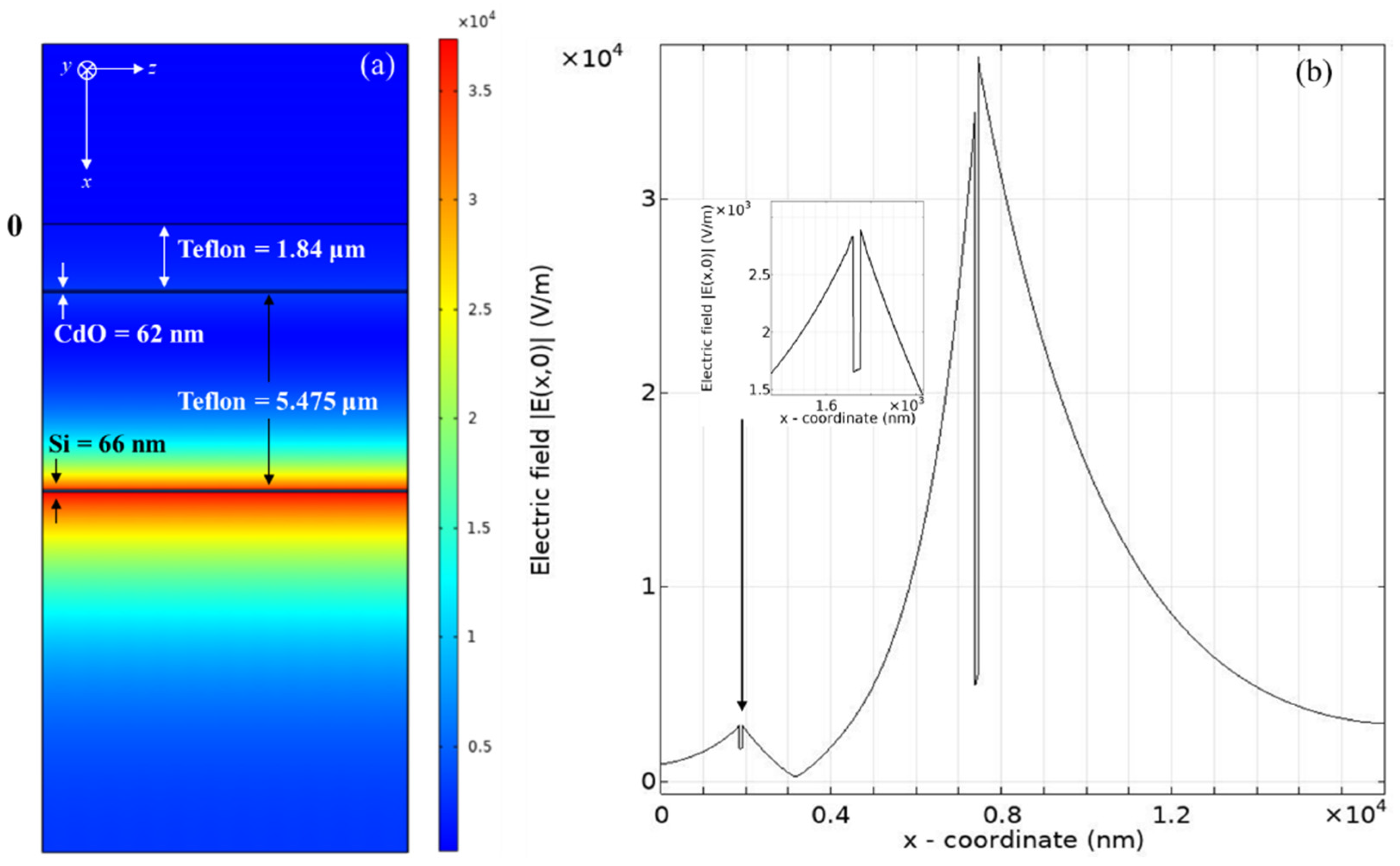
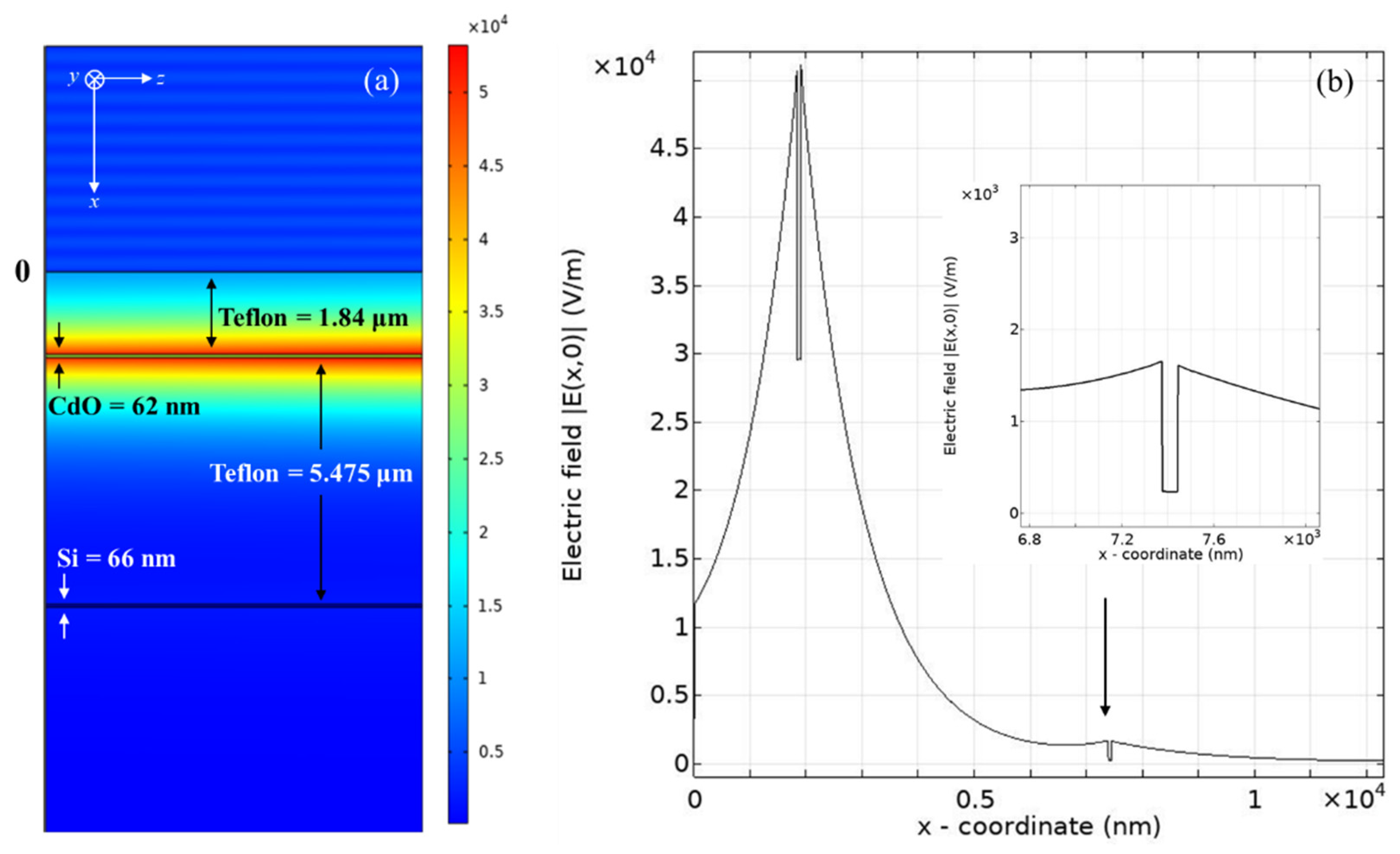
In order to verify the mode coupling between the LRSPP and DWG modes and to understand the origin of the Fano resonance, the surface electric field plot and electric field distribution of the sharp resonance (at point I) and broad resonance (at point II) in Figure 6a were obtained by using the finite element method (FEM)-based commercial software COMSOL Multiphysics 5.3. In our calculation, the computational window is large enough (−5 μm ≤ x ≤ 16 μm and −4 μm ≤ z ≤ 4 μm), and the perfect electric conductor boundary condition is used. For point I at the resonance angle of 32.4275°, the surface electric field and the distribution of the electric field are displayed in Figure 7a,b. One can clearly see the noticeable field at both CdO/Teflon interfaces (see the insert of Figure 7b) and strong field at the interfaces of the Teflon/Si and Si/analyte, which confirms the constructive field at interfaces of the DWG due to the field interference between the LRSPP mode and DWG mode, resulting in a sharp asymmetric Fano resonance lineshape. The point II at a resonance angle of 32.5717° indicates the excitation of the LRSPP mode, which is verified by the strong electric field distribution at both CdO/Teflon interfaces as shown in Figure 8a,b, where the mode of the DWG is almost suppressed, as seen in the inset of Figure 8b.

Figure 7.
(a) Surface electric field and (b) the corresponding electric field distribution at the incident angle of 32.4275° in the proposed six-layer hybrid structure.
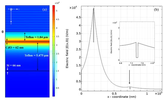
Figure 8.
(a) Surface electric field and (b) the corresponding electric field distribution at the incident angle of 32.5717° in the proposed six-layer hybrid structure.
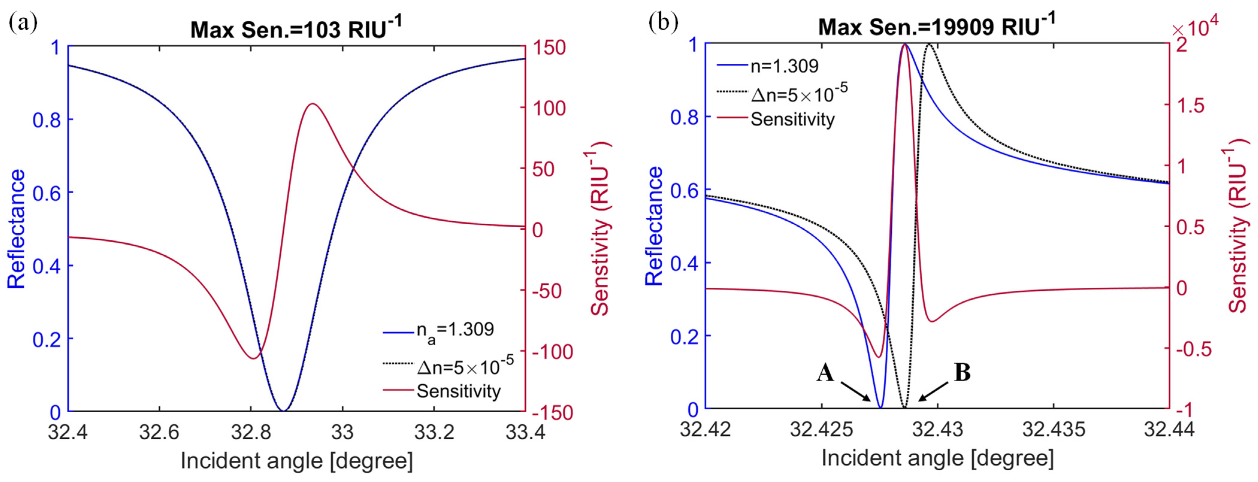
For comparison, the reflectance and sensitivity were calculated using Equations (9) and (10) for both the 4-layer LRSPR-based and the proposed 6-layer Fano resonance-based sensors, as shown in Figure 9a,b, respectively. For the 4-layer conventional LRSPR sensor with index variation of ∆n = 5 × 10⁻⁵, the thicknesses of the Teflon and CdO were set to 1.653 μm and 62 nm, and the refractive index of the sensing medium was 1.309. For the 4-layer structure, from Figure 9a, one can see that the resonance angle occurs at 32.8708°, and the maximum sensitivity is only 103 RIU−1. Figure 9b shows the reflectance and sensitivity of the proposed 6-layer Fano resonance-based sensor with the thicknesses setting given for Figure 6a. The sharp asymmetric Fano resonance dip exhibits at 32.4275° (point A). By setting the change in sensing medium index ∆n = 5 × 10⁻⁵, the Fano resonance moves to the right with the resonance angle at 32.4286° (point B), resulting in a maximum sensitivity of 19,909 RIU−1, which demonstrates significantly improved sensitivity compared to the conventional 4-layer LRSPR-based sensors mentioned above. Compared to the previously reported sensors [11,12,37,38,39,40,53], the proposed Fano resonance hybrid waveguide-coupled plasmonic senor shows significantly high sensitivity. Note that the near-infrared TCO-based sensors [37,38,39,40] are designed for operating at 1550 nm. The proposed sensor makes use of CdO as the plasmonic material, which allows us to extend the operating window to a longer wavelength at 1890 nm.
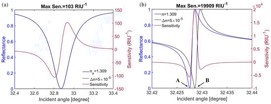
Figure 9.
Variation of reflectance and sensitivity with the incident angle for (a) the 4-layer LRSPR based sensor and (b) the proposed 6-layer Fano resonance-based sensor.
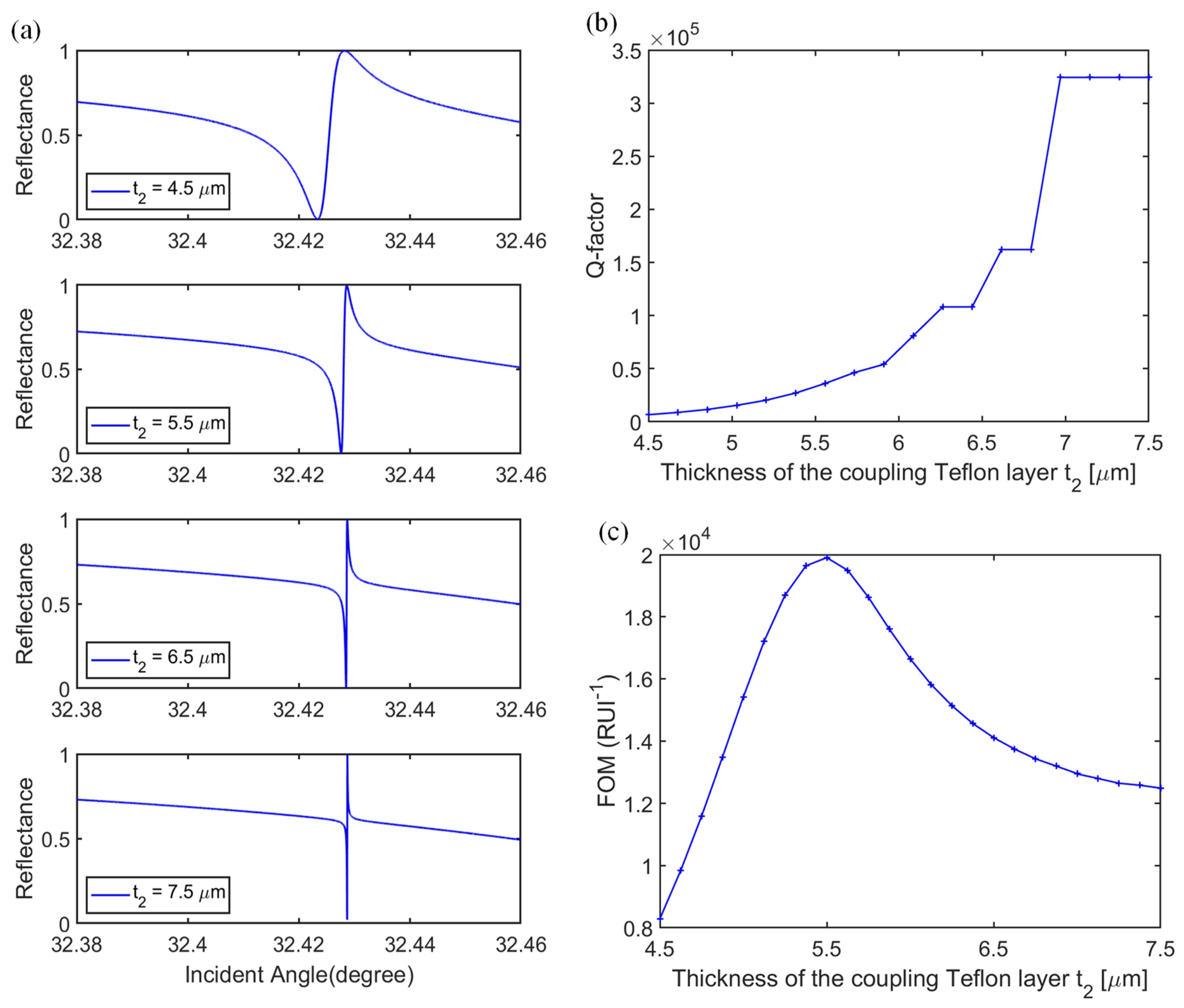
Next, the influences of the physical parameters on the Fano resonance were examined. We first considered the impact of the thickness of the coupling layer on the Fano resonance with all other structural parameters fixed at the optimized thicknesses mentioned above. Figure 10a shows the reflectance as a function of the incident angles for different coupling thicknesses t2 = 4.5 μm, 5.5 μm, 6.5 μm, and 7.5 μm. With increasing coupling layer thickness, the Fano asymmetric spectrum becomes sharper, which is attributed to the gradually decreased coupling strength between the LRSPP and DWG modes [13]. For example, at t2 = 4.5 μm, the Fano resonance has a broader lineshape, while when t2 = 5.5 μm, a much narrower linewidth is obtained. However, further increasing the coupling layer thickness (e.g., t2 = 7.5 μm), the reflectance of the Fano resonance dip cannot reach zero due to the weakened mode coupling strength between the LRSPP mode and the DWG mode. The Q-factor defined in Equation (11) as the ratio of the resonance angle θ to the angle difference ∆θ between the dip and peak, increases with increasing the thickness of the coupling layer, as shown in Figure 10b, which is expected to be due to the reduced linewidth of the resonance spectrum. Note that at a large coupling layer thickness, a high Q-factor is not an indicator of high sensitivity because of weak coupling strength to support the DWG mode, as can be seen from Figure 10c for the dependence of the FOM (i.e., maximum of sensitivity) on the thickness of the coupling layer. The optimum thickness of the coupling layer is around 5.475 μm, where the FOM can reach as high as 19,909 RIU−1. When t2 is larger than 5.475 μm, the FOM is gradually degraded.
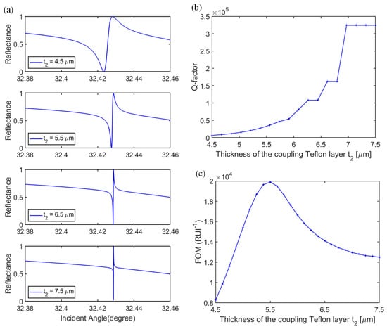
Figure 10.
(a) ATR curves of the Fano resonance for different thicknesses of the coupling Teflon layer t2; (b) Q-factor and (c) FOM as a function of the thickness of the coupling Teflon layer t2.
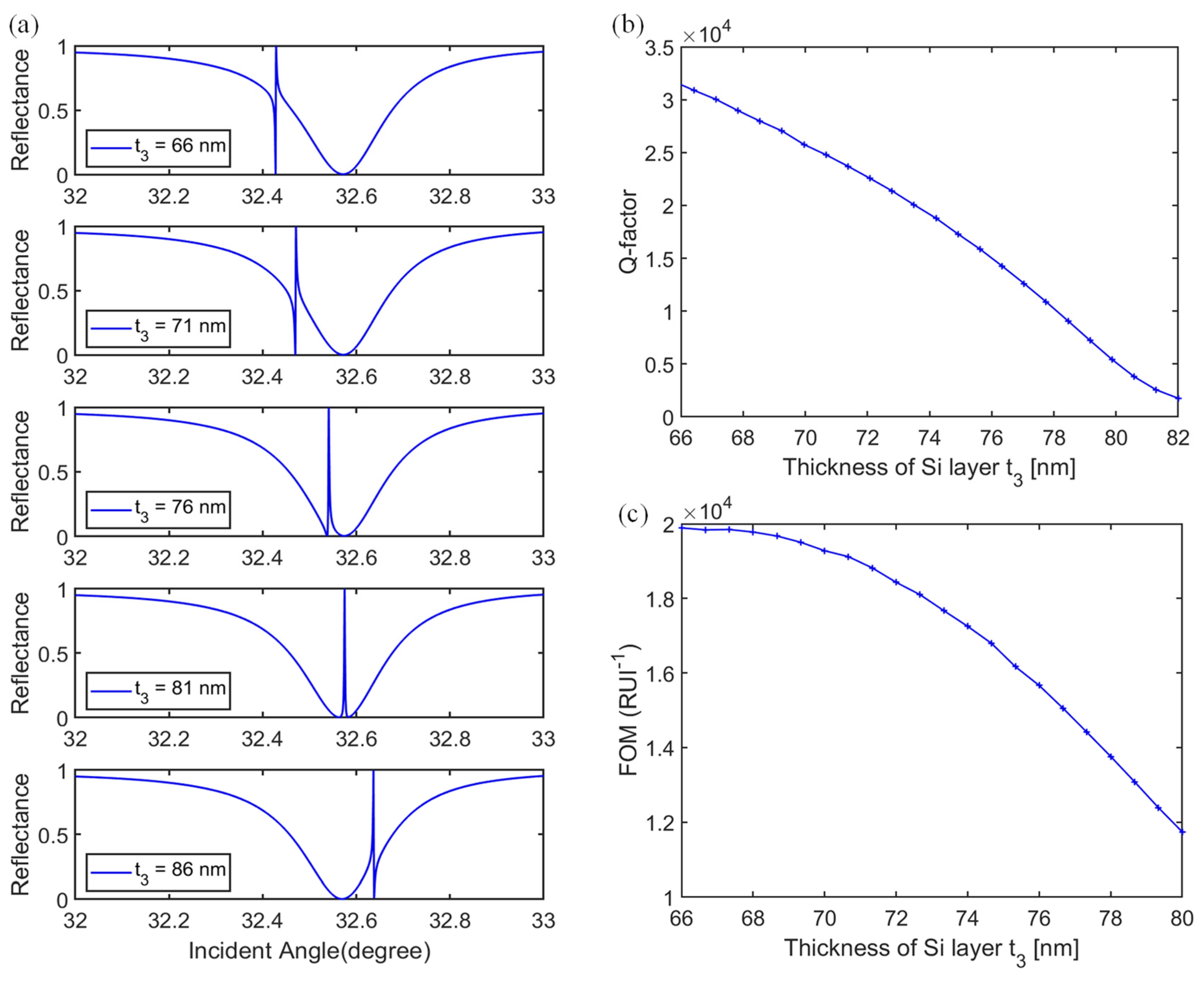
The effect of the thickness of the Si layer t3 on the Fano resonance was also investigated. Figure 11a shows the ATR spectra for the variation of t3 from 66 nm to 86 nm. When t3 is increased, the Fano resonance dip shifts to the larger angles and approaches the broad LRSPR resonance dip. At t3 = 81 nm, the distinct Fano resonance dip disappears; instead, the ATR curve appears to have a symmetric lineshape with a PIT window at an incident angle of 32.5749°. Further increasing t3, the Fano resonance dip appears again and shifts further to the right side of the LRSPR broad dip. For the DWG, when t3 increases, the modal index of the DWG mode increases, which leads to the movement of the Fano resonance dip to the larger angles. With an increase in the Si thickness, the Q-factor decreases and FOM degrades, as shown in Figure 11b,c.
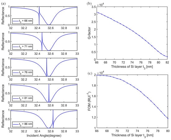
Figure 11.
(a) The movement of the Fano resonance dip, (b) variation of Q-factor, and (c) FOM with Si thickness increased from 66 nm to 86 nm.
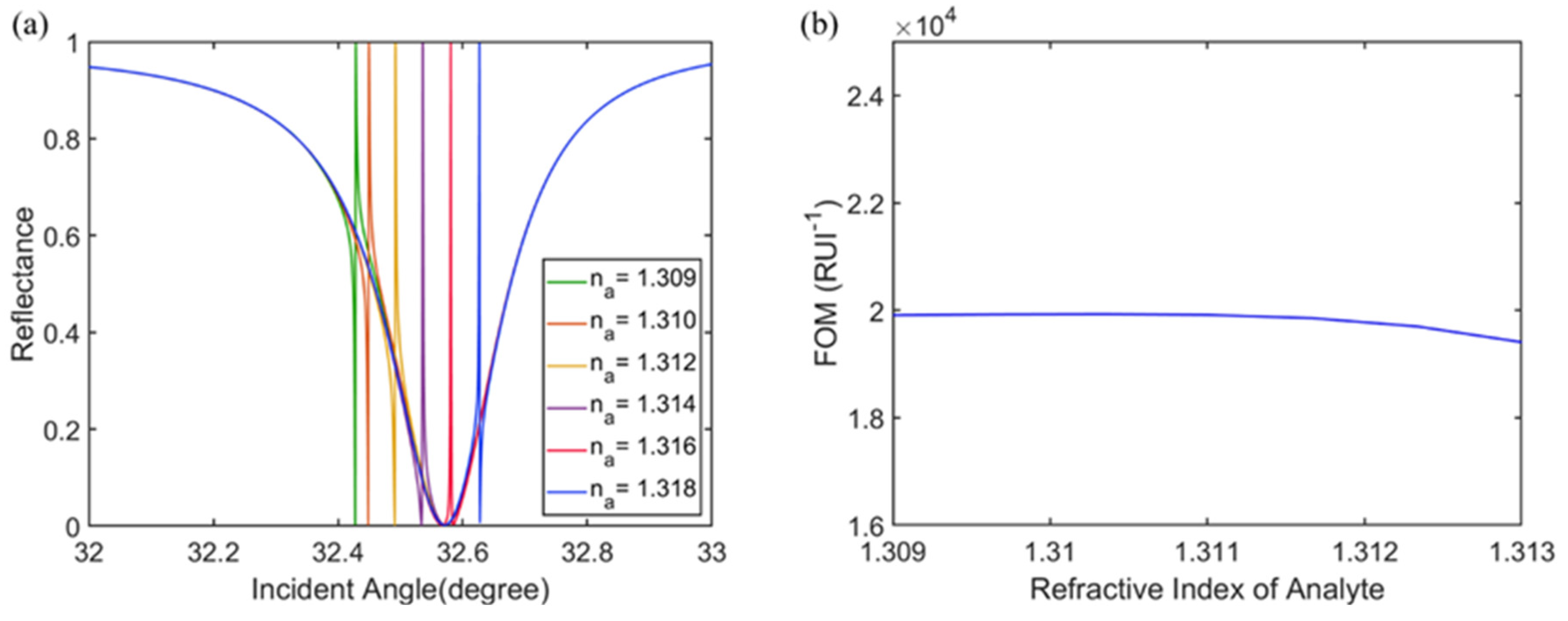
For sensing applications, when chemical or biological reactions occur in the sensing medium, the refractive index of the sensing medium is bound to change slightly. Figure 12a shows the ATR spectrum with respect to the change in the refractive index of the sensing medium. As can be seen, the resonance dip shifts to a large incident angle when increasing the index of the sensing medium. FOM as high as 19,909 RIU−1 can be achieved with the refractive index of the sensing medium ranging from 1.309 to 1.313, as shown in Figure 12b.
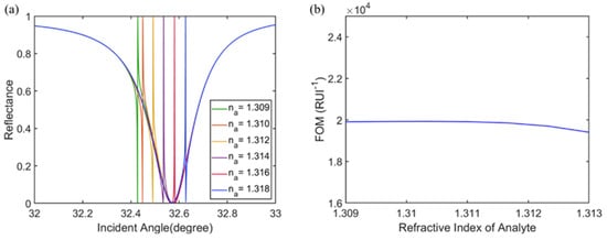
Figure 12.
(a) The movement of the Fano resonance dip for the different index of the sensing medium and (b) variation of FOM with respect to the refractive index of the sensing medium.
4. Conclusions
In this paper, a waveguide-coupled LRSPR system is proposed using transparent conducting material CdO as the plasmonic material for refractive index sensing in the near-infrared range. The proposed ultrasensitive sensor is based on Fano resonance, originating from the strong coupling between the DWG mode (supported by 3-layer asymmetric Teflon/Si/Water structure) and the LRSPP mode (supported by a 4-layer asymmetric ZnSe/Teflon/CdO/Teflon structure). The design procedures for determining and optimizing the physical dimensions of the inner four layers are elaborated. The results show that the thicknesses of the inner layers play an important role in creating the Fano resonance and PIT. With optimized physical parameters, FOM (i.e., maximum intensity sensitivity) of 19,909 RIU−1 could be achieved in the Fano resonance-based scheme, which is a 193-fold enhancement compared to conventional 4-layer LRSPR based schemes. The proposed CdO-based hybrid plasmonic structure provides an excellent platform for near-infrared sensing technology, finding potential applications for biological detection, chemical reaction, food safety, and environmental monitoring near-infrared regions.
Author Contributions
Conceptualization, A.K. and L.W.; Methodology, A.K. and L.W.; Software, A.K.; Formal analysis, A.K. and L.W.; Supervision, L.W.; Writing, A.K. and L.W. All authors have read and agreed to the published version of the manuscript.
Funding
This research was funded in part by the Natural Sciences and Engineering Research Council of Canada (NSERC) and Wilfrid Laurier University.
Institutional Review Board Statement
Not applicable.
Informed Consent Statement
Not applicable.
Data Availability Statement
Not applicable.
Conflicts of Interest
The authors declare no conflict of interest.
References
- Otto, A. Excitation of nonradiative surface plasma waves in silver by the method of frustrated total reflection. Z. Phys. 1968, 216, 398–410. [Google Scholar] [CrossRef]
- Kretschmann, E.; Raether, H. Notizen: Radiative decay of non-radiative surface plasmons excited by light. Z. Naturforsch. A 1968, 23, 2135–2136. [Google Scholar] [CrossRef]
- Daghestani, H.N.; Day, B.W. Theory and Applications of Surface Plasmon Resonance, Resonant Mirror, Resonant Waveguide Grating, and Dual Polarization Interferometry Biosensors. Sensors 2010, 10, 9630–9646. [Google Scholar] [CrossRef] [PubMed]
- Lee, K.S.; Lee, T.S.; Kim, I.; Kim, W.M. Parametric study on the bimetallic waveguide coupled surface plasmon resonance sensors in comparison with other configurations. J. Phys. D Appl. Phys. 2013, 46, 125302. [Google Scholar] [CrossRef]
- Lahav, A.; Auslender, M.; Abdulhalim, I. Sensitivity enhancement of guided-wave surface-plasmon resonance sensors. Opt. Lett. 2008, 33, 2539–2541. [Google Scholar] [CrossRef] [PubMed]
- Shalabney, A.; Abdulhalim, I. Figure-of-merit enhancement of surface plasmon resonance sensors in the spectral interrogation. Opt. Lett. 2012, 37, 1175–1177. [Google Scholar] [CrossRef] [PubMed]
- Wu, L.; Ling, Z.; Jiang, L.; Guo, J.; Dai, X.; Xiang, Y.; Fan, D. Long-range surface plasmon with graphene for enhancing the sensitivity and detection accuracy of biosensor. IEEE Photonics J. 2016, 8, 4801409. [Google Scholar] [CrossRef]
- Xu, Y.; Hsieh, C.H.; Wu, L.; Ang, L.K. Two-dimensional transition metal dichalcogenides mediated long range surface plasmon resonance biosensors. J. Phys. D Appl. Phys. 2019, 52, 065101. [Google Scholar] [CrossRef] [Green Version]
- Sarid, D. Long-range surface-plasma waves on very thin metal films. Phys. Rev. Lett. 1981, 47, 1927. [Google Scholar] [CrossRef]
- Berini, P. Long-range surface plasmon polaritons. Adv. Opt. Photonics 2009, 1, 484–588. [Google Scholar] [CrossRef]
- Wu, L.; Guo, J.; Xu, H.; Dai, X.; Xiang, Y. Ultrasensitive biosensors based on long-range surface plasmon polariton and dielectric waveguide modes. Photonics Res. 2016, 4, 262–266. [Google Scholar] [CrossRef]
- Li, L.; Huang, T.; Zhao, X.; Wu, X.; Cheng, Z. Highly sensitive SPR sensor based on hybrid coupling between plasmon and potonic mode. IEEE Photonics Technol. Lett. 2018, 30, 1364–1367. [Google Scholar] [CrossRef]
- Hayashi, S.; Nesterenko, D.V.; Sekkat, Z. Waveguide-coupled surface plasmon resonance sensor structures: Fano lineshape engineering for ultrahigh-resolution sensing. J. Phys. D Appl. Phys. 2015, 48, 325303. [Google Scholar] [CrossRef]
- Hayashi, S.; Nesterenko, D.V.; Sekkat, Z. Fano resonance and plasmon-induced transparency in waveguide-coupled surface plasmon resonance sensors. Appl. Phys. Express 2015, 8, 022201. [Google Scholar] [CrossRef] [Green Version]
- Hayashi, S.; Nesterenko, D.V.; Rahmouni, A.; Sekkat, Z. Observation of Fano line shapes arising from coupling between surface plasmon polariton and waveguide modes. Appl. Phys. Lett. 2016, 108, 051101. [Google Scholar] [CrossRef] [Green Version]
- Nesterenko, D.V.; Hayashi, S.; Sekkat, Z. Extremely narrow resonances, giant sensitivity and field enhancement in low-loss waveguide sensors. J. Opt. 2016, 18, 065004. [Google Scholar] [CrossRef]
- Sekkat, Z.; Hayashi, S.; Nesterenko, D.V.; Rahmouni, A.; Refki, S.; Ishitobi, H.; Inouye, Y.; Kawata, S. Plasmonic coupled modes in metal-dielectric multilayer structures: Fano resonance and giant field enhancement. Opt. Express 2016, 24, 20080–20086. [Google Scholar] [CrossRef] [PubMed]
- Zheng, G.; Cong, J.; Xu, L.; Wang, J. High-resolution surface plasmon resonance sensor with Fano resonance in waveguide-coupled multilayer structures. Appl. Phys. Express 2017, 10, 042202. [Google Scholar] [CrossRef]
- Ruan, B.; You, Q.; Zhu, J.; Wu, L.; Guo, J.; Dai, X.; Xiang, Y. Fano resonance in double waveguides with graphene for ultrasensitive biosensor. Opt. Express 2018, 26, 16884. [Google Scholar] [CrossRef] [PubMed]
- Jiang, H.; Zheng, G.; Rao, W. Ultra-sensitive biosensor with hybrid coupling between molybdenum disulfide thin film and photonic waveguide mode. Results Phys. 2019, 13, 102173. [Google Scholar] [CrossRef]
- Chao, C.T.C.; Chau, Y.F.C.; Chiang, H.P. Multiple Fano resonance modes in an ultra-compact plasmonic waveguide-cavity system for sensing applications. Results Phys. 2021, 27, 104527. [Google Scholar] [CrossRef]
- Chau, Y.F.C.; Chao, C.T.C.; Jumat, S.Z.B.H.; Kooh, M.R.R.; Thotagamuge, R.; Lim, C.M.; Chiang, H.P. Improved Refractive Index-Sensing Performance of Multimode Fano-Resonance-Based Metal-Insulator-Metal Nanostructures. Nanomaterials 2021, 11, 2097. [Google Scholar] [CrossRef] [PubMed]
- Rybin, M.V.; Khanikaev, A.B.; Inoue, M.; Samusev, K.B.; Steel, M.J.; Yushin, G.; Limonov, M.F. Fano resonance between Mie and Bragg scattering in photonic crystals. Phys. Rev. Lett. 2009, 103, 023901. [Google Scholar] [CrossRef] [PubMed] [Green Version]
- Pradarutti, B.; Torosyan, G.; Theuer, M.; Beigang, R. Fano profiles in transmission spectra of terahertz radiation through one dimensional periodic metallic structures. Appl. Phys. Lett. 2010, 97, 244103. [Google Scholar] [CrossRef]
- Khan, A.D.; Miano, G. Higher order tunable Fano resonances in multilayer nanocones. Plasmonics 2013, 8, 1023–1034. [Google Scholar] [CrossRef]
- Hoang, T.T.; Ngo, Q.M.; Vu, D.L.; Nguyen, H.P.T. Controlling Fano resonances in multilayer dielectric gratings towards optical bistable devices. Sci. Rep. 2018, 8, 16404. [Google Scholar] [CrossRef] [Green Version]
- Zhao, G.; Zhao, T.; Xiao, H.; Liu, Z.; Liu, G.; Yang, J.; Ren, Z.; Bai, J.; Tian, Y. Tunable Fano resonances based on microring resonator with feedback coupled waveguide. Opt. Express 2016, 24, 20187–20195. [Google Scholar] [CrossRef]
- Limonov, M.F.; Rybin, M.V.; Poddubny, A.N.; Kivshar, Y.S. Fano resonances in photonics. Nat. Photonics 2017, 11, 543–554. [Google Scholar] [CrossRef]
- Lu, D.; Li, W.; Zhou, H.; Cao, X.; Wang, K.; Luo, H.; Li, J.; Zhang, X.; He, M.; Xu, L.; et al. Coupling between surface plasmon polariton and planar waveguide modes in the biosensor based on metal–insulator–metal/planar waveguide structure. Opt. Commun. 2020, 459, 124928. [Google Scholar] [CrossRef]
- Gu, L.; Fang, L.; Fang, H.; Li, J.; Zheng, J.; Zhao, J.; Zhao, Q.; Gan, X. Fano resonance lineshapes in a waveguide-microring structure enabled by an air-hole. APL Photonics 2020, 5, 016108. [Google Scholar] [CrossRef] [Green Version]
- Chen, J.; Gan, F.; Wang, Y.; Li, G. Plasmonic sensing and modulation based on Fano resonances. Adv. Optical Mater. 2018, 6, 1701152. [Google Scholar] [CrossRef]
- Stanley, R. Plasmonics in the mid-infrared. Nat. Photonics 2012, 6, 409–411. [Google Scholar] [CrossRef]
- Foteinopoulou, S.; Devarapu, G.C.R.; Subramania, G.S.; Krishna, S.; Wasserman, D. Phonon-polaritonics: Enabling powerful capabilities for infrared photonics. Nanophotonics 2019, 8, 2129–2175. [Google Scholar] [CrossRef] [Green Version]
- Naik, G.V.; Kim, J.; Boltasseva, A. Oxides and nitrides as alternative plasmonic materials in the optical range. Opt. Mater. Express 2011, 1, 1090–1099. [Google Scholar] [CrossRef] [Green Version]
- Khamh, H.; Sachet, E.; Kelly, K.; Maria, J.P.; Franzen, S. As good as gold and better: Conducting metal oxide materials for mid-infrared plasmonic applications. J. Mater. Chem. C. 2018, 6, 8326–8342. [Google Scholar] [CrossRef]
- Lee, H.W.; Papadakis, G.; Burgos, S.P.; Chander, K.; Kriesch, A.; Pala, R.; Peschel, U.; Atwater, H.A. Nanoscale conducting oxide PlasMOStor. Nano Lett. 2014, 14, 6463–6468. [Google Scholar] [CrossRef] [PubMed] [Green Version]
- Ruan, B.; You, Q.; Zhu, J.; Wu, L.; Guo, J.; Dai, X.; Xiang, Y. Improving the performance of an SPR biosensor using long-range surface plasmon of Ga-doped zinc oxide. Sensors 2018, 18, 2098. [Google Scholar] [CrossRef] [Green Version]
- Pal, S.; Verma, A.; Prajapati, Y.K.; Saini, J.P. Figure of merit enhancement of surface plasmon resonance biosensor using Ga-doped zinc oxide in near infrared range. Photonic Sens. 2020, 10, 340–352. [Google Scholar] [CrossRef] [Green Version]
- Pal, S.; Pal, N.; Verma, A.; Saini, J.P.; Prajapati, Y.K. Analyzing the role of Transparent conducting oxide in place of metals in SPR sensor for biomolecular detection in near infrared range. Results in Opt. 2021, 3, 100078. [Google Scholar] [CrossRef]
- Huang, T.; Zeng, S.; Zhao, X.; Cheng, Z.; Shum, P.P. Fano resonance enhanced surface plasmon resonance sensors operating in near-infrared. Photonics 2018, 5, 23. [Google Scholar] [CrossRef] [Green Version]
- Sachet, E.; Shelton, C.T.; Harris, J.S.; Gaddy, B.E.; Irving, D.L.; Curtarolo, S.; Donovan, B.F.; Hopkins, P.E.; Sharma, P.A.; Sharma, A.L.; et al. Dysprosium doped cadmium oxide: A gateway material for mid-infrared plasmonics. Nat. Mater. 2015, 14, 414–420. [Google Scholar] [CrossRef] [PubMed]
- Runnerstrom, E.L.; Kelley, K.P.; Sachet, E.; Shelton, C.T.; Maria, J.P. Epsilon-near-zero modes and surface plasmon resonance in Fluorine-doped Cadmium oxide thin films. ACS Photonics. 2017, 4, 1885–1892. [Google Scholar] [CrossRef]
- Yang, Y.; Kelley, K.; Sachet, E.; Campione, S.; Luk, T.S.; Maria, J.P.; Sinclair, M.B.; Brener, I. Femtosecond optical polarization switching using a cadmium oxide-based perfect absorber. Nat. Photonics 2017, 11, 390–395. [Google Scholar] [CrossRef]
- Salzberg, C.D.; Villa, J.J. Infrared Refractive Indexes of Silicon Germanium and Modified Selenium Glass. J. Opt. Soc. Amer. 1957, 47, 244. [Google Scholar] [CrossRef]
- Tatian, B. Fitting Refractive-index data with the Sellmeier dispersion formula. Appl. Opt. 1984, 23, 4477. [Google Scholar] [CrossRef] [PubMed]
- Yang, M.K.; French, R.H.; Tokarsky, E.W. Optical properties of Teflon (R) AF amorphous fluoropolymers. J. Micro/Nanolith. MEMS MOEMS. 2008, 7, 033010. [Google Scholar] [CrossRef]
- Equilateral Dispersive Prisms. ZnSe Equilateral Dispersive Prisms (600 nm–16 nm); Thorlabs, Inc.: Shanghai, China, 2012; Available online: www.thorlabs.com/newgrouppage9.cfm?objectgroup_id=148 (accessed on 14 March 2022).
- Huang, T.; Xu, G.; Pan, J.; Cheng, Z.; Shum, P.P.; Brambilla, G. Theoretical study of bicharacteristic waveguide for fundamental-mode phase-matched SHG from MIR to NIR. Opt. Express 2019, 27, 15236–15250. [Google Scholar] [CrossRef] [PubMed]
- Thulium-Doped Fiber Lasers: 1800 nm to 2050 nm; Thorlabs, Inc.: Shanghai, China, 2012; Available online: https://www.thorlabs.com/newgrouppage9.cfm?objectgroup_id=11137 (accessed on 14 March 2022).
- Yamamoto, M. Surface plasmon resonance (SPR) theory: Tutorial. Rev. Polarogr. (JPN) 2002, 48, 209–237. [Google Scholar] [CrossRef]
- Hansen, W.H. Electric fields produced by the propagation of plane coherent electromagnetic radiation in a stratified medium. J. Opt. Soc. Am. 1968, 58, 380–388. [Google Scholar] [CrossRef]
- Srivastava, T.; Jha, R. Black Phosphorus: A New Platform for Gaseous Sensing Based on Surface Plasmon Resonance. IEEE Photon. Technol. Lett. 2018, 30, 319–322. [Google Scholar] [CrossRef]
- Zhang, X.; Wang, Y.; Zhao, X.; Huang, T.; Zeng, S.; Ping, P.S. Fano resonance based on long range surface phonon resonance in the mid-infrared region. IEEE Photonics J. 2019, 11, 4800808. [Google Scholar] [CrossRef]
- Hale, G.M.; Querry, M.R. Optical constants of water in the 200-nm to 200-µm wavelength region. Appl. Opt. 1973, 12, 555–556. [Google Scholar] [CrossRef] [PubMed]


Publisher’s Note: MDPI stays neutral with regard to jurisdictional claims in published maps and institutional affiliations. |
© 2022 by the authors. Licensee MDPI, Basel, Switzerland. This article is an open access article distributed under the terms and conditions of the Creative Commons Attribution (CC BY) license (https://creativecommons.org/licenses/by/4.0/).