Article

Sunlight Communication System Built with Tunable 3D-Printed Optical Components

1
Graduate Institute of Photonics and Optoelectronics, National Taiwan University, Taipei 10617, Taiwan
2
Department of Electrical Engineering, National Taiwan University, Taipei 10617, Taiwan
*
Author to whom correspondence should be addressed.
Photonics 2022, 9(3), 188; https://doi.org/10.3390/photonics9030188
Submission received: 25 January 2022 / Revised: 11 March 2022 / Accepted: 14 March 2022 / Published: 16 March 2022
(This article belongs to the Special Issue Advances in Optical Wireless Technologies and Applications)

Abstract

:
In this paper, optical components are fabricated using a 3D printing method. The two following strategies are adopted: 1. combining 3D printing, “origami”, and metal coating/attaching to directly manufacture parabolic reflectors; 2. inserting mirrors into 3D-printed frames and assembling the mirrors to form a corner cube retroreflector (CCR). PDLC (polymer dispersed liquid crystal) films are integrated with these optical components to achieve voltage-controlled optical power modulation. The tunable CCR is used to construct a solar light communication system. Using sunlight directly as the light source for communication is rarely seen. In this paper, we demonstrate a proof of concept of sunlight communication, exploring a new route of solar energy utilization, in addition to electricity generation and heating.

1. Introduction

Wireless communication has been a popular topic for recent years. This study combines sunlight, 3D printing technology, and polymer dispersed liquid crystal (PDLC) to demonstrate a proof of concept for solar communication in free space. The research and development of solar energy utilization has always focused on solar power generation and solar heat collection. Efforts have been diverted to seeking other possible utilizations of solar power. For example, sunlight has been used as a pump source to build lasers [1,2]; although such lasers may not look very practical for the time being, they do offer possibilities for the future. As far as we know, it is quite rare to use sunlight as a light source for communication. In this study, we hope to open up another path for the usage of solar energy, and we expect to be able to apply the research results of this paper to temporary communication stations, ship communication and even space communication.
Visible light can be used as a light source for lighting, and also as a carrier wave for free space communication [3,4,5,6,7]. Visible light communication is a Li-Fi technology; the term Li-Fi is a counterpart of the term Wi-Fi for radio-wave wireless networks. Compared with radio waves, visible light provides the benefits of wider bandwidths, high confidentiality (high directivity), high popularity (illumination light sources can be seen everywhere), etc. These advantages provide potential for developing visible light communication. As for the use of sunlight as a light source for communication, inexhaustible solar energy is most attractive. The total solar irradiance received by the Earth is about 1.36 kW/m2 [8].
In this study, we manufacture components for solar communication in a fast and cost-effective manner. We choose fused deposition modeling (FDM) 3D printing. FDM 3D printing offers low cost, large printing areas, and fast printing speeds; it is environmentally friendly because it does not require the use of powder and photo-curable polymers as other printing technologies do. To accomplish the modulation mechanism, polymer dispersed liquid crystal (PDLC) is selected and can be used to adjust the transmitted light intensity by changing the applied voltage. Although the modulation speed is not fast, it is sufficient for a proof of concept. Moreover, the manufacturing cost of the PDLC is low, which means that it does not require expensive equipment, and can be fabricated in a normal laboratory rather than a clean room environment.
In our earlier trial we combined the 3D printing, “origami”, PDLC modulation layer and metal reflective layer to directly manufacture all optical components. However, in the process of developing the corner cube retroreflector (CCR) [9], we found that the origami method required a very large printing area which could easily cause serious warpage, and therefore mirror curvature. Moreover, the mirror–mirror connection could be easily damaged due to its small thickness and the large 90-degree bending angle as shown in Figure 1a. Therefore, we redesigned the CCR and adopted the latching–assembling approach as shown in Figure 1b.
With this modified approach, CCR parts can be printed separately so that the printing areas are smaller so as to reduce warpage, and all parts are assembled via latching mechanisms. 3D printing is used to print the frame, and then a purchased mirror is inserted into the frame, as displayed in Figure 2a. This can ensure good flatness and reflectivity of the three CCR mirrors. The CCR formed by the three assembled mirrors is shown in Figure 2b. As for the parabolic mirror, the main structure is still directly made by the 3D printing method, and is later integrated with the PDLC modulation layer and metal reflective layer.

2. Component Fabrication

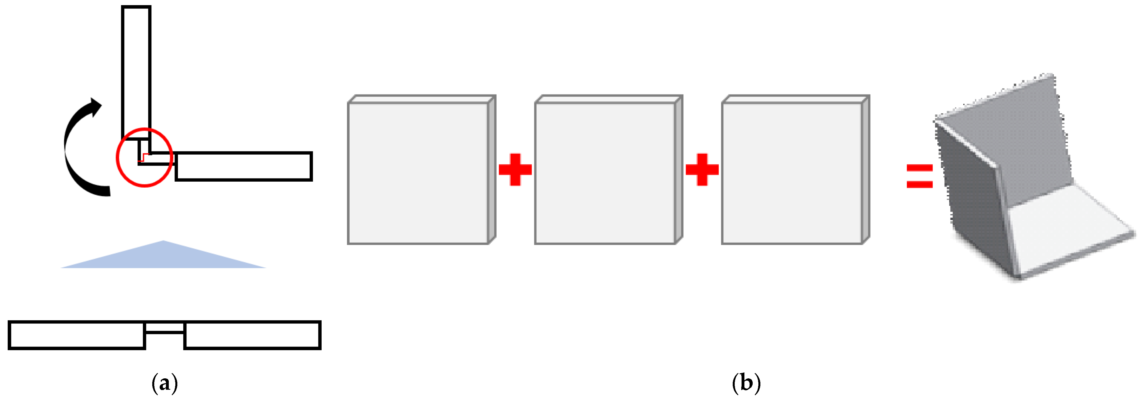
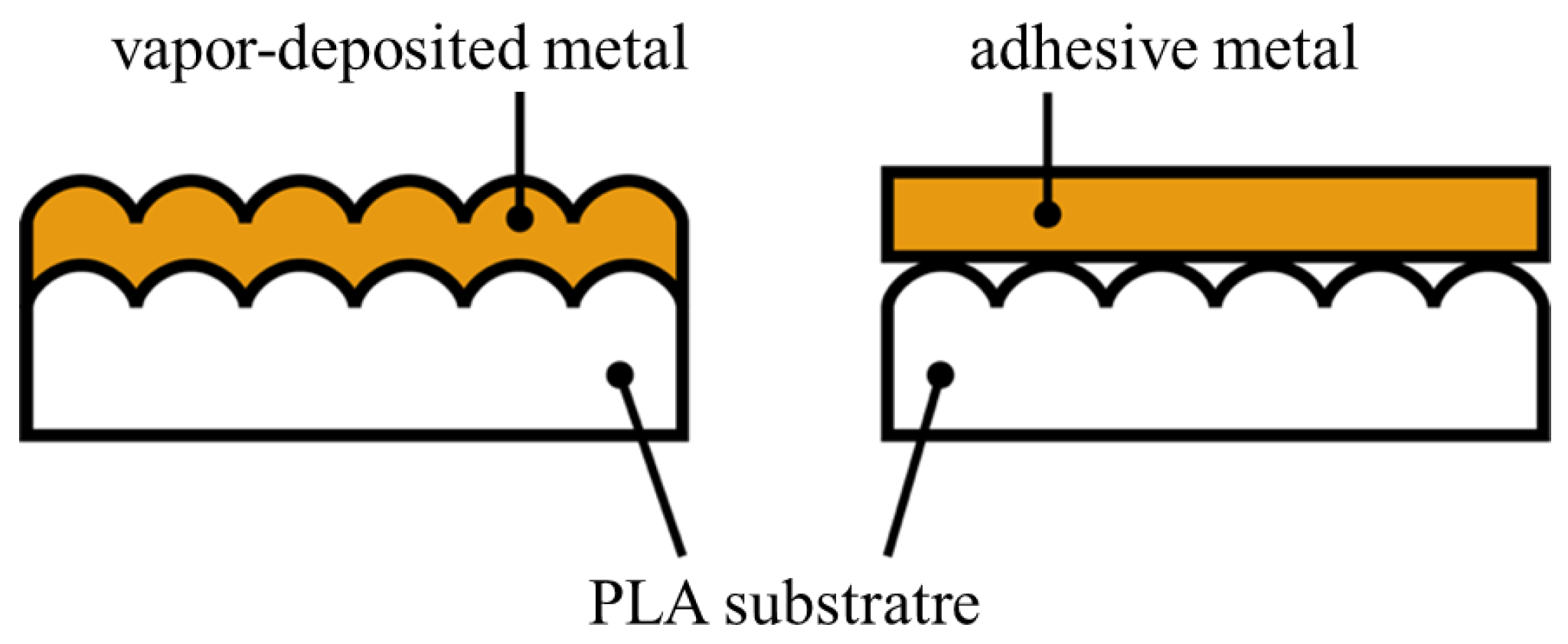
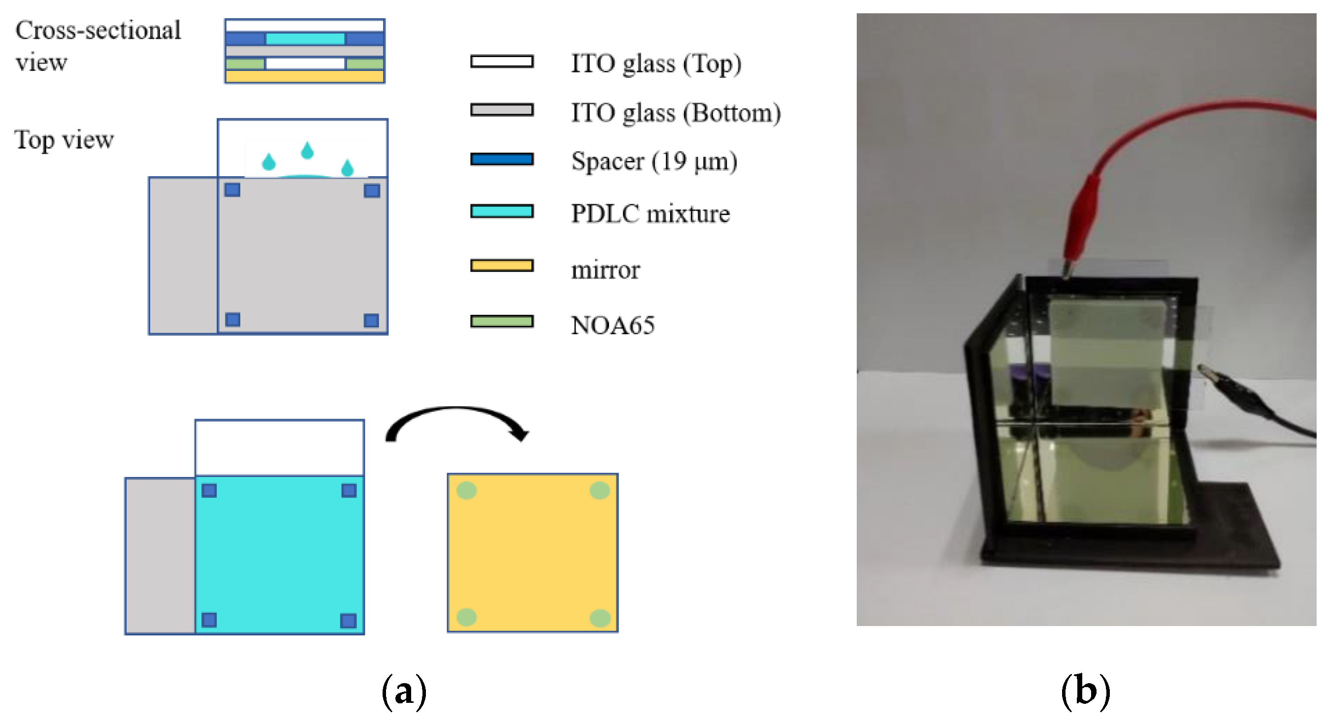
2.1. Parabolic Mirror (Strictly Speaking, Paraboloid-like Mirror)

It is necessary to fabricate the substrate, metal reflective layer, and PDLC modulation layer in the parabolic mirror-manufacturing process. The substrate design is drawn using 3D modeling software, and then the substrate is FDM 3D-printed. The substrate material is PLA, which is environmentally friendly. The FDM 3D printer normally produces periodic ruggedness on the surface. There are two approaches in constructing a metal reflective layer, as shown in Figure 3. The first is to use an evaporation–deposition process that directly deposits aluminum onto the PLA surface; the second is to attach a conductive copper tape to the PLA surface.
The PDLC in this study is made by UV-curing the mixture of E7 liquid crystal (Merck) and Norland Optical Adhesive 65 (NOA65). The weight ratio of E7 to NOA65 is 6:4. The E7 liquid crystal and NOA65 adhesive are mixed at room temperature; uniform mixing can be achieved in about five minutes with agitation. The wavelength of the UV exposure unit is around 380 nm; the unit contains six UV lamps, each with a rated power consumption of 15 W. When using the first approach, the vapor-deposited aluminum layer inherits the surface ruggedness of the PLA substrate, making it difficult to fabricate the PDLC module directly on top of the aluminum. Therefore, the modulation module needs to be made separately. Flat and flexible ITO films (i.e., ITO coated on transparent flexible plastic-like films) are used as the upper and lower electrodes of the PDLC modulation layer. The fabricated modulation module is then glued to the metal reflective layer by NOA65, and the whole piece is then folded and fixed on a parabolic support/bracket. The detailed step-by-step procedure is shown in Figure 4 and is as follows: 1. Print the PLA substrate and deposit aluminum by thermal evaporation; 2. Spread the mixture of E7 and NOA65 on the lower ITO film [10] and place in a vacuum chamber for 2 h; 3. Cover with the upper ITO Film [10] and wait for the mixture to fill the gap completely; 4. After the filling is complete, place a weight (i.e., the transparent glass) on the modulation module and perform UV exposure for 6 min; 5. The cured modulation module is trimmed to fit the shape of the PLA substrate and glued to the reflective metal layer by NOA65; 6. Use a parabolic bracket to assist folding to form a tunable parabolic mirror and use glue (manufacturer: 3M Company) to fix the parabolic mirror onto the bracket. For readers’ reference, the PET (polyethylene terephthalate) films for spacers in Figure 4 are acquired from a local company.
With the second approach that attaches a copper tape to the PLA substrate, there is no topography transfer as with the first approach; the copper tape can serve as the lower electrode itself. Therefore, the step-by-step procedure is modified as follows: 1. Print the PLA substrate and attach a copper tape as the metal reflective layer; 2. Spread the mixture of E7 and NOA65 on the copper tape and place in a vacuum chamber for 2 h; 3. Cover with the upper ITO Film and wait for the mixture to fill the gap completely; 4. After the filling is complete, place a weight on the device and perform UV exposure for 6 min; 5. Use a parabolic bracket to assist folding to form a tunable parabolic mirror and use glue (manufacturer: 3M Company) to fix the parabolic mirror onto the bracket.
Figure 5a shows the two parabolic mirrors before actuation; the left uses the vapor-deposited aluminum as the reflective material while the right uses the copper tape. Without actuation, the milky PDLC lessens the shine of the observed metal. In Figure 5b, photos of the device after applying voltage are provided. Under actuation, the PDLC transmittance increases and the metal surfaces can be seen more clearly.

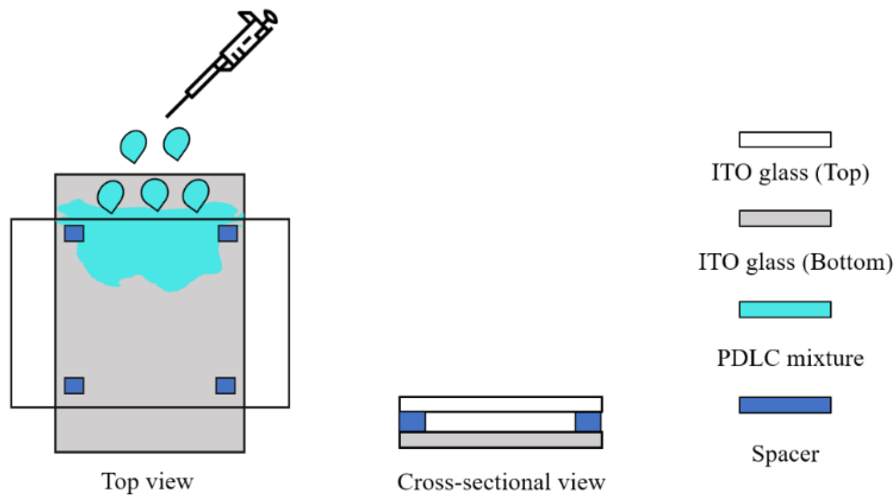
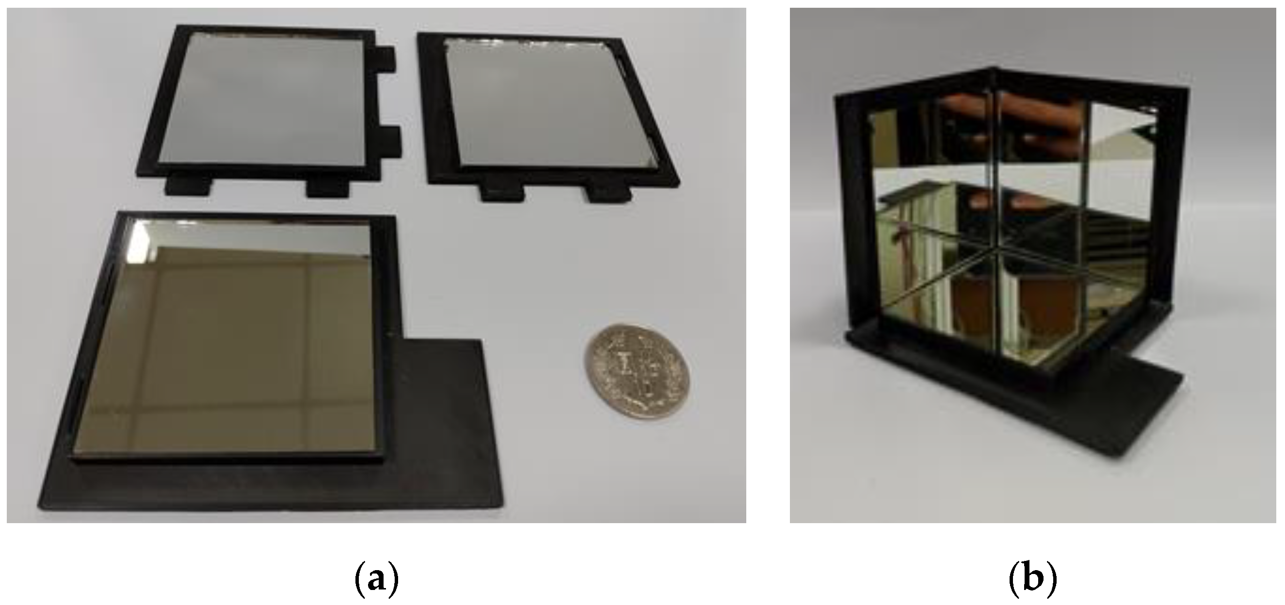
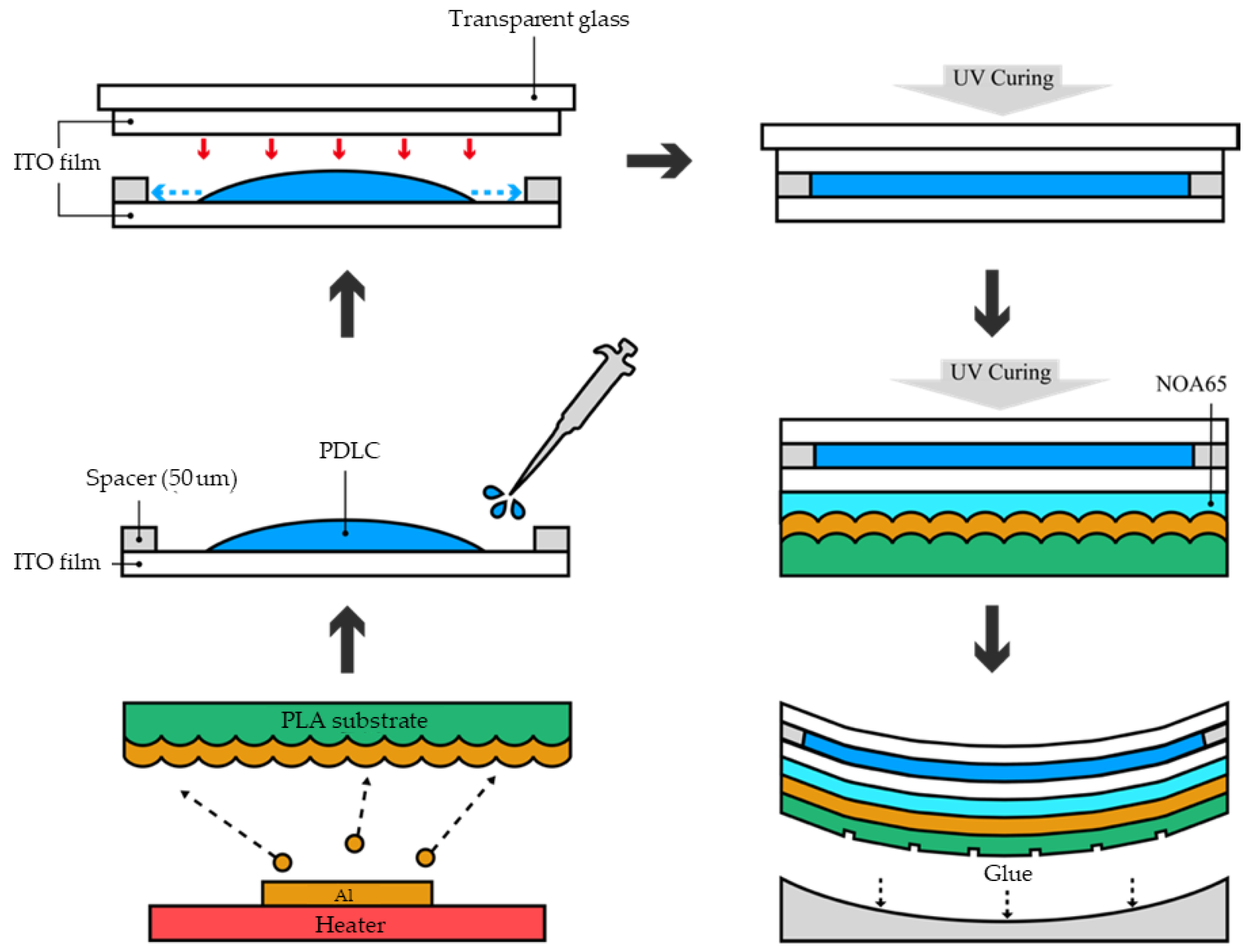
2.2. Corner Cube Retroreflector (CCR)

The specification and manufacturing process of the PDLC modulation module for the CCR are as follows. Two 5 cm × 7 cm pieces of ITO glass (ITO coated on glass; the overlap area of the two pieces is 5 cm × 5 cm) and polyethylene terephthalate (PET) spacers of 19 um thickness are used. The reason for choosing ITO glass of such a large area is to increase the light-accepting area. We then fill the gap between the ITO glass substrates with the PDLC mixture (i.e., the uncured mixture of E7 + NOA65) via the capillary action as shown in Figure 6; the advantage of utilizing the capillary action is that the amount of mixture required can be more precisely determined so that less waste is produced. Then, the mixture is UV-cured. The results show that the ON state (voltage amplitude = 150 V (1 kHz)) in Figure 7a and the OFF state (no applied voltage) in Figure 7b are quite different through bare-eye inspection, which meets our expectation.
For readers’ reference, one of our earlier PDLC modules with a 12 μm thick PDLC layer showed a transmittance of <3% at an applied voltage amplitude of 5 V (1 kHz); its transmittance reached >75% when the applied voltage amplitude was raised to 100 V (1 kHz) [11]. Due to the large areas required for the parabolic mirrors and CCR in this study, the spacers, and therefore, the PDLC layers, need to be thicker to prevent physical contact between the ITO layers during the fabrication process, at the cost of higher ON-state voltages and lower transmittance.
Although it is time-consuming to utilize the capillary action (requiring about 40 min on average), the thickness of PDLC can be determined more accurately (by the spacer thickness) because the two pieces of ITO glass are positioned and separated by spacers before injecting the PDLC mixture.
After completing the fabrication of the modulation module, NOA65 is applied to the four corners of one CCR mirror to attach the PDLC module with glue, as shown in Figure 8a. The reason for using NOA65 is that it is transparent, colorless and viscous, and can be cured with ultraviolet light. It is worth mentioning that the retro-reflection of a CCR is achieved by allowing the light to be reflected by all the three mirrors one by one. Therefore, it is only necessary to place a modulation module on one mirror (Figure 8b) to control the retro-reflected optical power from the CCR.

3. Results and Discussion

3.1. Device Characterization

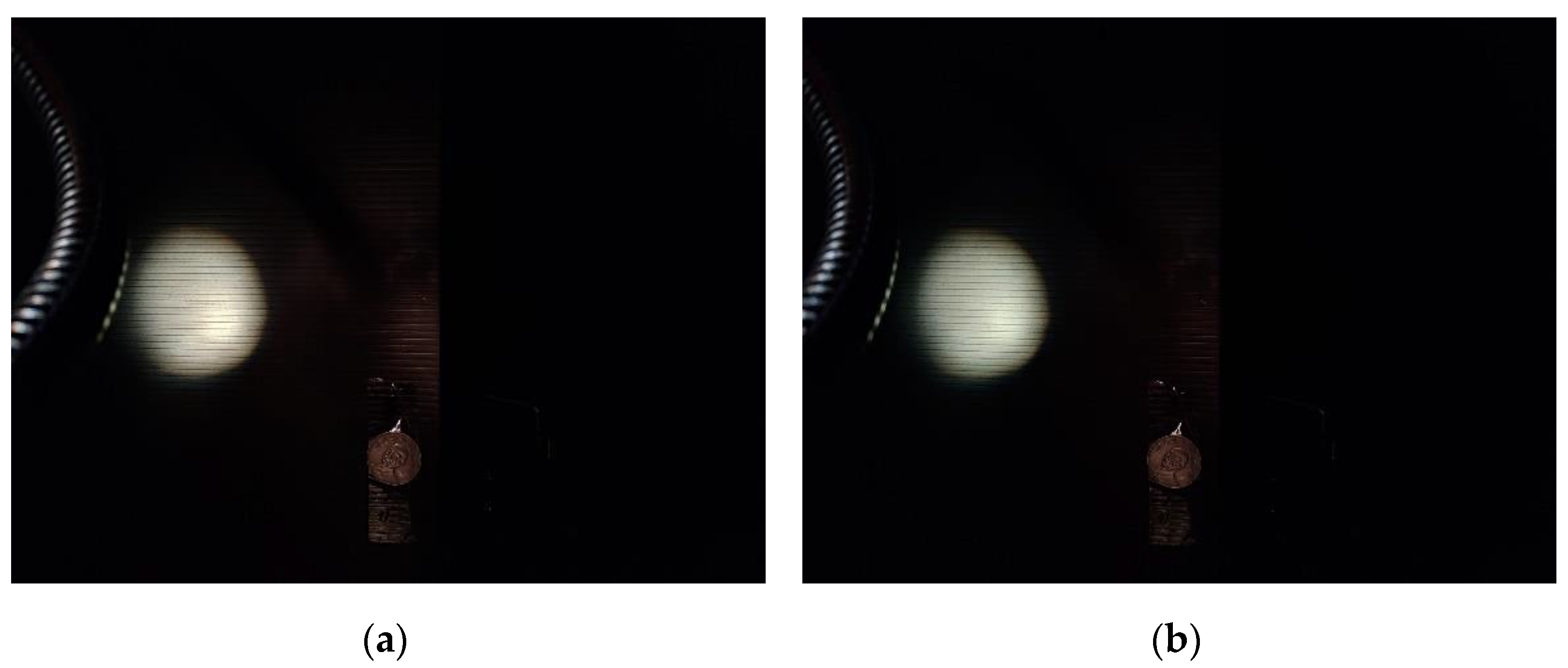
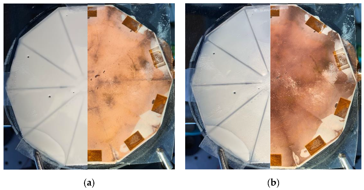
3.1.1. Parabolic Mirror

For the parabolic mirrors, we measure the reflected optical power versus driving voltage (voltage amplitude). In the measurement setup, a white light halogen lamp is used as the light source. The light is collimated (to approximate sunlight incident onto the Earth) using a lens. It is then shined on and reflected by the parabolic mirror at a small incident angle, and is focused on the detector of an optical power meter. A function generator outputs a sinusoidal voltage of 1 kHz, and the voltage is amplified by 50X for application on the devices. The reflected optical power versus voltage amplitude is plotted for both parabolic mirrors in Figure 9. We define the voltage at the red arrow as the actuation voltage of the ON state. The contrast is defined as the ratio of the ON-state optical power (at the actuation voltage) to that of the OFF state (at 0 V):
Contrast = ONState   Optical   Power OFFState   Optical   Power × 100 %
The parabolic mirror with an attached copper tape exhibits a lower actuation voltage, partly because the bottom electrode is copper which has a lower resistance than ITO. It should be noted that the final voltage applied to the aluminum-coated parabolic mirror is a 1 kHz sinusoidal waveform that oscillates between 0 and X volts, which is composed of the 50X amplified sinusoidal waveform and a dc bias. On the other hand, the voltage applied to the copper-tape parabolic mirror is a 1 kHz sinusoidal waveform oscillating between −X~X volts. In Figure 9, the value along the horizontal axis represents the X value.
The copper-tape parabolic mirror also exhibits better contrast, partly due to the fact that the copper tape is attached to the PLA substrate to serve as the reflecting layer and does not inherit the PLA surface ruggedness exhibited by the vapor-deposit aluminum. This could be the reason for its higher reflected optical power, which results in a better contrast. Table 1 provides a comparison between the two devices.

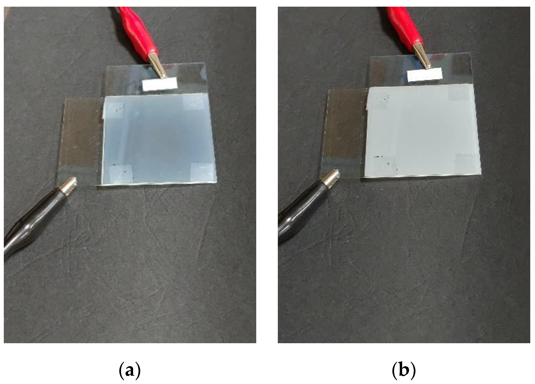
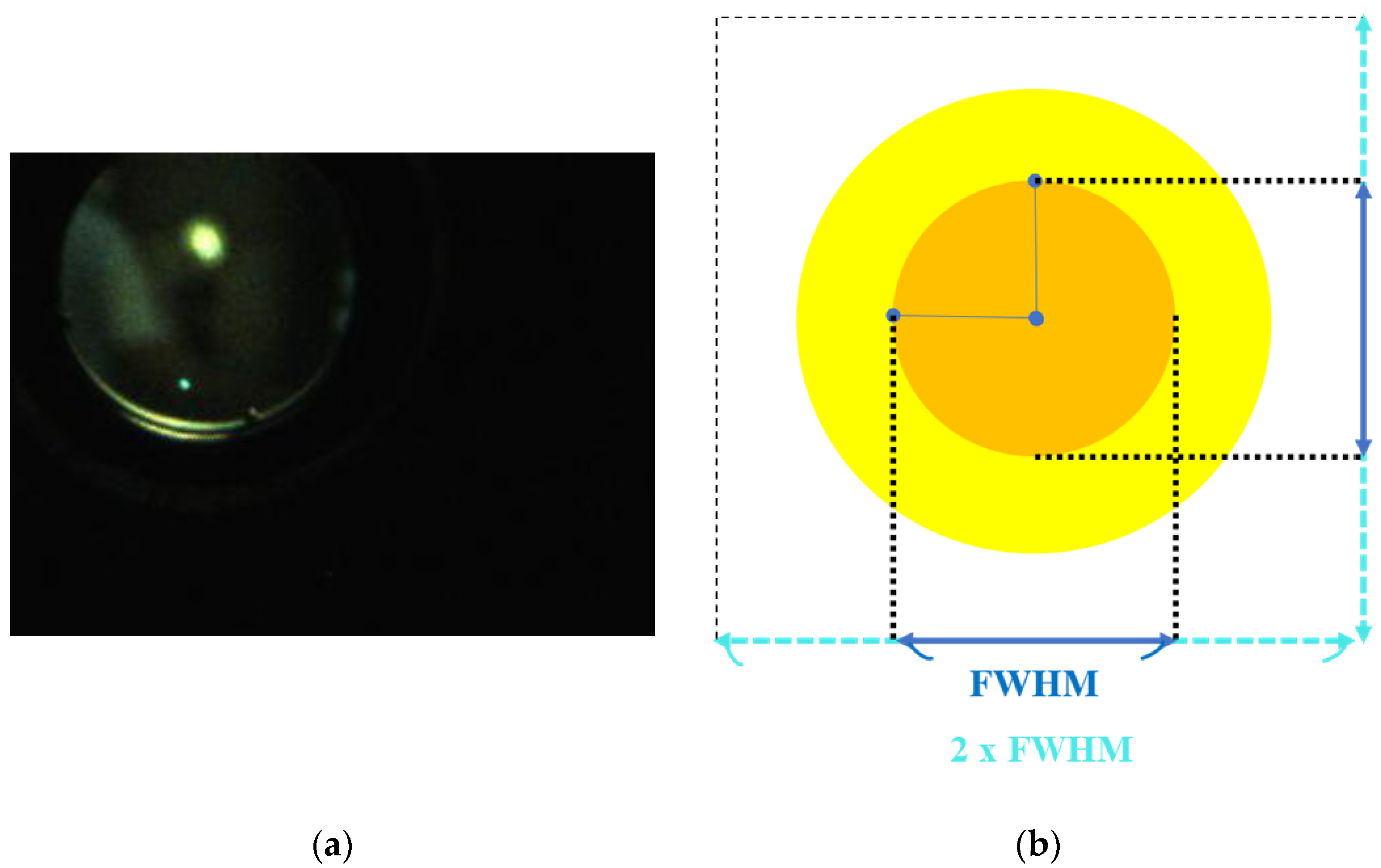
3.1.2. Cube Corner Retroreflector (CCR)

The measurement setup for the CCR is similar to that for the parabolic mirrors. The collimated white light is shined on one CCR mirror. After three reflections, it is retro-reflected back along the direction parallel to the incoming path. Due to an offset between the incoming and return paths, we are able to place a screen behind the light source for observation. Similarly, a 1 kHz sinusoidal waveform is output by the function generator, and amplified by 50X. Changing the voltage amplitude allows the PDLC modulation module to switch between the ON and OFF states. Figure 10 shows the huge light spot on the screen. It can be observed, by the bare eye, that the brightness of the ON state (with applied voltage) is slightly higher than that of the OFF state. The low contrast is partially due to the fact that the top ITO glass surface itself produces some reflected light, the power of which does not change with the voltage.
To obtain the contrast, we place the detector (aperture diameter: 9.5 mm) of an optical power meter in front of the screen to measure the optical power. We still define the contrast as the optical power ratio between the ON state and OFF state:
Contrast = ONState   Optical   Power OFFState   Optical   Power
At the ON state of a voltage amplitude of 120 V, the contrast is about 1.11. Although the contrast is not high, it is sufficient to demonstrate a proof of concept for the proposed system.

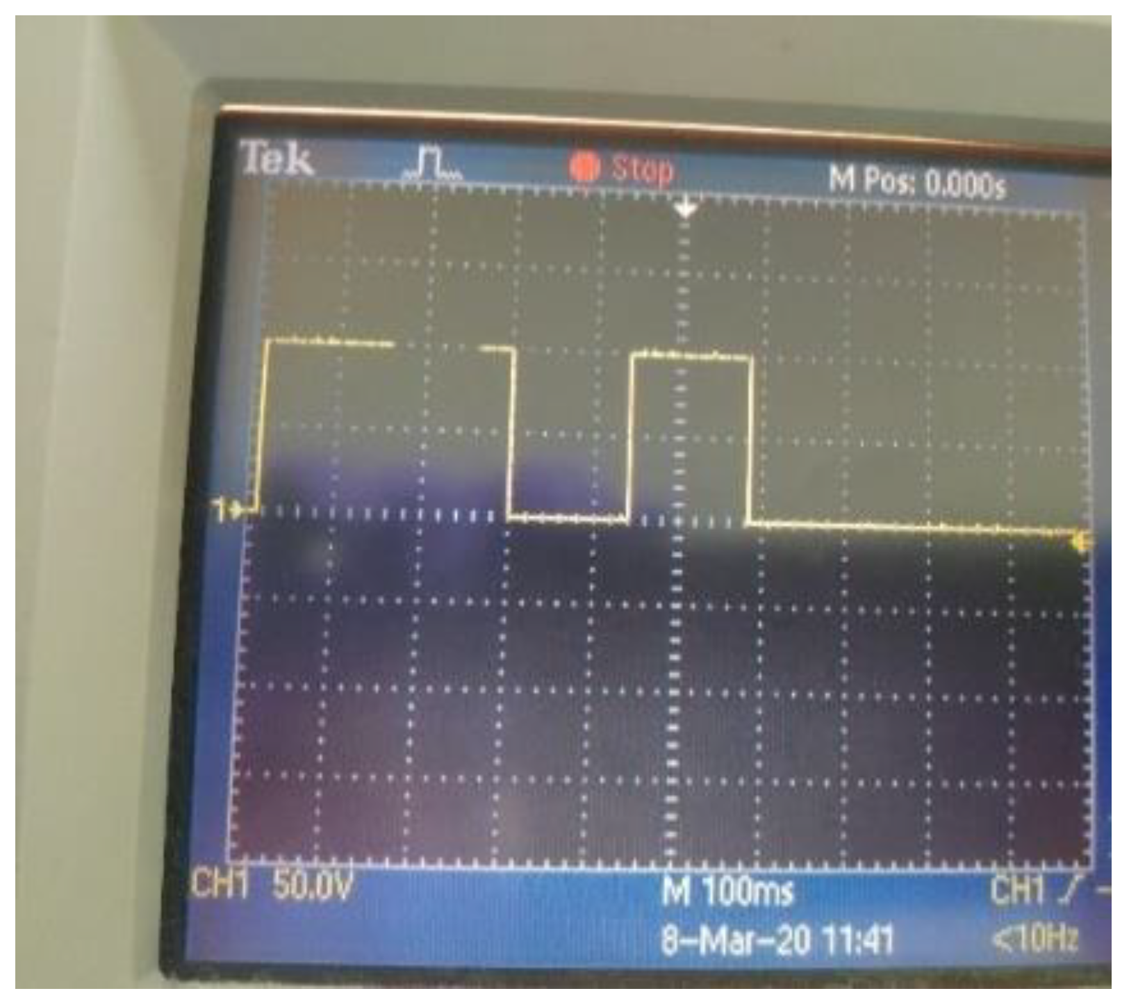
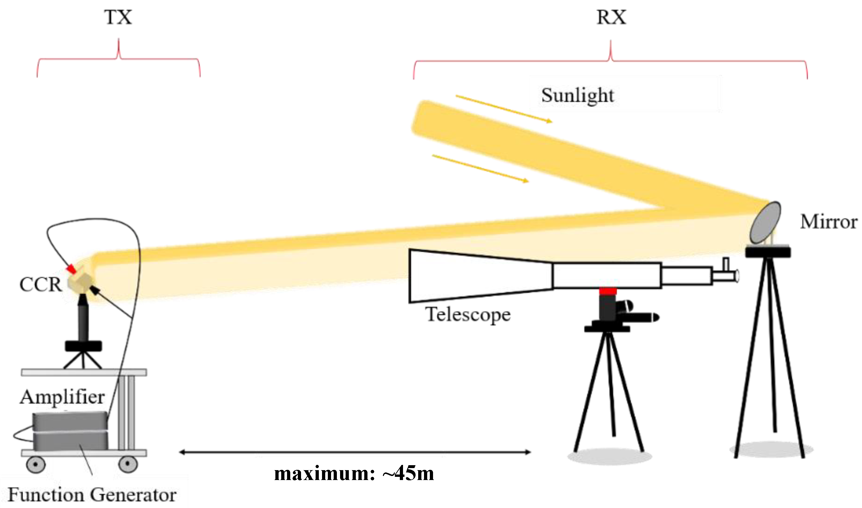
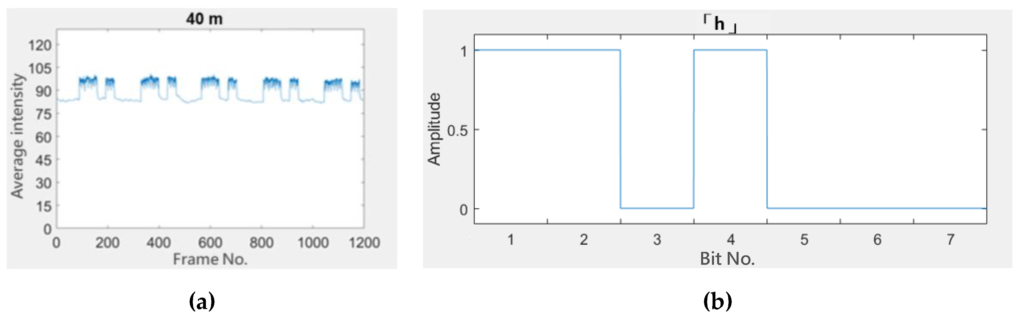
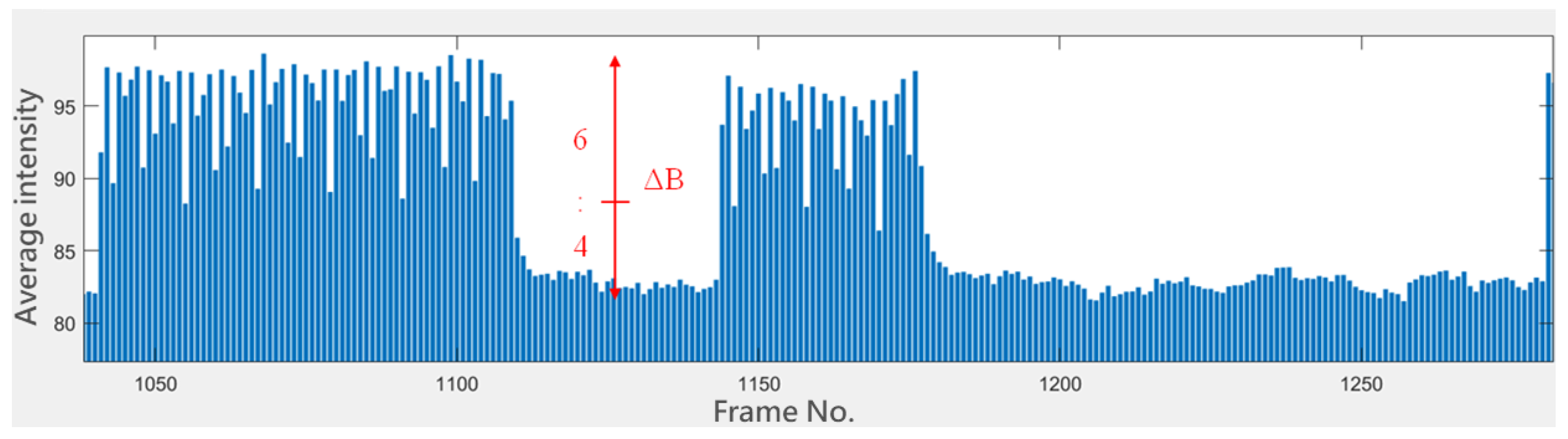
3.2. System Setup and Transmission Test

We choose the CCR and use a telescope (Meade LXD75 EMC) equipped with a camera to build the prototype free-space sunlight communication system. At the current stage, the maximum transmission distance is about 45 m. Figure 11 provides a schematic diagram of the prototype setup. In addition to the telescope and industrial camera, the receiver (RX) is also equipped with a mirror to reflect sunlight to the CCR of the transmitter (TX), and the light modulated by the CCR is then retroreflected to the telescope and industrial camera.
At the TX unit, an amplified 1 kHz sinusoidal voltage, which can be considered as a carrier wave, is fed to the CCR. We use the OOK (on-off keying) modulation to deliver the data. When the carrier wave is present, the PDLC is turned on and a stronger reflected light can be detected at the RX unit; this represents the delivery of a binary 1. On the other hand, when the carrier wave is absent, the PDLC is switched off and the reflected optical power is lower; this represents receiving a binary 0 at the RX unit. Figure 12 shows the binary ASCII code of the character “h” displayed on an oscilloscope; this type of waveform will be used to modulate the carrier wave to control the state of the PDLC.
At the RX unit, the camera records in the low-resolution high-frame-rate mode. Image analyses and data restoration are performed later using Matlab. Figure 13a provides a raw image (one frame) acquired at a TX-RX distance of 40 m; Figure 13b illustrates how the region of interest for analysis is determined. We first convert the raw image into a grayscale version, and calculate the full width at half maximum (FWHM) of the light spot in the upper left of Figure 13a, in both directions, and define a rectangular area around the light spot whose length and width are twice the FWHMs in the horizontal and vertical directions, respectively (Figure 13b).
Then, we calculate the average grayscale intensity within the region of interest of each frame; the results of repeatedly transmitting the character “h” are plotted in Figure 14a. Figure 14b presents a typical binary ASCII waveform of the character “h” for comparison. Figure 14a can be further converted into a bar chart such as Figure 15. In Figure 15, where the results of one transmitted “h” are presented, we select brightest frame and the darkest frame; their average intensities are indicated by the levels of upper and lower ends of the red arrow, respectively; the length of the arrow represents the intensity difference ΔB. A red horizontal line divides the arrow into two segments with a length ratio of 6:4. For frames with average intensities that exceed the level of this horizontal line are regarded as 1 s, and those with average intensities below this level are regarded as 0 s.
Since this is our very first field test of the outdoor sunlight free-space communication prototype system, we used a simple way to determine the maximum allowable working distance. At a certain distance, the character “h” (1101000) is transmitted five times (totally 35 bits in 5 s). If the 35 bits of the five “h” cannot be fully restored, that distance is considered non-workable. With this method, we determine that the maximum working distance for the time being is approximately 45 m.

4. Conclusions

This study utilized 3D printing technology to manufacture two types of optical components: 1. Using 3D printing and origami to directly fabricate a metal-coated or metal-attached parabolic mirror; 2. Inserting mirrors into 3D-printed frames and forming a corner cube retroreflector (CCR) by assembly. Both components were integrated with polymer dispersed liquid crystal (PDLC) modules, and the reflected/retro-reflected light power can be adjusted by changing the applied voltage. We selected the above CCR component to construct a free space communication system using sunlight as the light source (also referred to as a solar communication system).
The research and development of solar energy utilization has focused on solar power generation and solar heating or heat collection. It is quite rare to use sunlight as a light source for communication. This paper demonstrates a proof of concept of sunlight communication, exploring a new path for the usage of solar energy.
We believe the working distance is mainly limited by the CCR modulation contrast for the time being. If the contrast can be further improved, it is expected that the working distance can be extended. Finally, the modulation frequency of PDLC is generally in the order of about 0.1 kHz, which limits the transmission speed. In the future, an array of components may be used to boost the transmission speed.

Author Contributions

Conceptualization, J.-c.T.; experiment, C.-K.S., W.-T.C., Y.-H.W. and K.-Y.L.; writing, C.-K.S. and J.-c.T. All authors have read and agreed to the published version of the manuscript.

Funding

This research was supported by the Ministry of Science and Technology of Taiwan under Grant MOST 107-2221-E-002-115-MY2, Grant MOST 109-2221-E-002-019 and Grant MOST 110-2221-E-002-076.

Data Availability Statement

Data supporting the results reported in this paper may be obtained from the authors upon reasonable request.

Conflicts of Interest

The authors declare no conflict of interest.

References

  1. Liang, D.; Almeida, J. Highly efficient solar-pumped Nd:YAG laser. Opt. Express 2011, 19, 26399–26405. [Google Scholar] [CrossRef] [PubMed]
  2. Guan, Z.; Zhao, C.M.; Yang, S.H.; Wang, Y.; Ke, J.Y.; Zhang, H.Y. Demonstration of a free-space optical communication system using a solar-pumped laser as signal transmitter. Laser Phys. Lett. 2017, 14, 055804. [Google Scholar] [CrossRef]
  3. Gunawan, W.-H.; Liu, Y.; Chow, C.-W.; Chang, Y.-H.; Yeh, C.-H. High speed visible light communication using digital power domain multiplexing of orthogonal frequency division multiplexed (OFDM) signals. Photonics 2021, 8, 500. [Google Scholar] [CrossRef]
  4. Nie, Y.; Zhang, W.; Yang, Y.; Deng, X.; Liu, M.; Chen, C. Pairwise coded mCAP with chaotic dual-mode index modulation for secure bandlimited VLC systems. Photonics 2022, 9, 141. [Google Scholar] [CrossRef]
  5. Zhan, L.; Zhao, H.; Zhang, W.; Lin, J. An optimal scheme for the number of mirrors in vehicular visible light communication via mirror array-based intelligent reflecting surfaces. Photonics 2022, 9, 129. [Google Scholar] [CrossRef]
  6. Miao, P.; Yin, W.; Peng, H.; Yao, Y. Study of the performance of deep learning-based channel equalization for indoor visible light communication systems. Photonics 2021, 8, 453. [Google Scholar] [CrossRef]
  7. Yang, Y.-C.; Yeh, C.-H.; Liaw, S.-K.; Chow, C.-W.; Hsu, W.-H.; Wang, B.-Y. Analysis and investigation of dual-polarized color LED based visible light communication system. Photonics 2021, 8, 210. [Google Scholar] [CrossRef]
  8. Kopp, G.; Lean, J.L. A new, lower value of total solar irradiance: Evidence and climate significance. Geophys. Res. Lett. 2011, 38, L01706. [Google Scholar] [CrossRef] [Green Version]
  9. Lai, K.Y.; Chen, W.T.; Wu, Y.H.; Chen, Y.F.; Tsai, J.C. 3D-printed and PDLC-tuned corner cube retro-reflector for sunlight communication. In Proceedings of the 2019 International Conference on Optical MEMS and Nanophotonics, Daejeon, Korea, 28 July–1 August 2019; pp. 164–165. [Google Scholar]
  10. EFUN Technology Co., LTD. Product: ITO. Available online: https://www.efun.com.tw/prod_intro/ito-%E9%80%8F%E6%98%8E%E5%B0%8E%E9%9B%BB%E8%86%9C (accessed on 18 January 2022).
  11. Chen, H.H.; Gu, J.H.; Lai, Y.X.; Lee, W.C.; Tsai, J.C. Digital Photography Using a High-Transmittance Electro-Optical Iris. IEEE Photonics J. 2019, 11, 1–8. [Google Scholar] [CrossRef]
Figure 1. (a) The mirror–mirror connection of the CCR could be easily damaged when using the origami method in our earlier trial. (b) With the modified approach in this paper, separate parts are assembled using latching mechanisms (latching mechanisms not shown in the figure).
Photonics 09 00188 g001
Figure 2. (a) 3D printing is used to print the frame, after which a purchased mirror is inserted into the frame; the protrusions in the photo are for the latches. (b) CCR is formed after assembling.
Photonics 09 00188 g002
Figure 3. The difference between the two metal-layer-making processes. Vapor-deposited metal inherits the substrate topography, which leads to periodic ruggedness, whereas attaching a metal tape can bypass this issue.
Photonics 09 00188 g003
Figure 4. Step-by-step procedure in which the first approach (evaporation deposition) is used: 1. Print the PLA substrate and deposit aluminum by thermal evaporation; 2. Spread the mixture of E7 and NOA65 on the lower ITO film and place in a vacuum chamber for 2 h; 3. Cover with the upper ITO Film and wait for the mixture to fill the gap completely; 4. After the filling is complete, place a weight on the modulation module and perform UV exposure for 6 min; 5. The cured modulation module is trimmed to fit the shape of the PLA substrate and glued to the reflective metal layer by NOA65; 6. Use a parabolic bracket to assist folding to form a tunable parabolic mirror and use glue (manufacturer: 3M Company) to fix the parabolic mirror onto the bracket.
Photonics 09 00188 g004
Figure 5. (a) Two parabolic mirrors before actuation; the left uses the vapor-deposited aluminum as the reflective material while the right uses the copper tape. (b) Device photos after applying voltage; under actuation, the metal surfaces can be seen more clearly. The diameter of the parabolic mirrors is ~8.8 cm.
Photonics 09 00188 g005
Figure 6. The PDLC modulation module for the CCR made by the capillary action.
Photonics 09 00188 g006
Figure 7. Photos of the fabricated PDLC modulation module: (a) ON state, voltage amplitude = 150 V (1 kHz), (b) OFF state, no applied voltage.
Photonics 09 00188 g007
Figure 8. (a) The combination of the PDLC modulation module and one of the CCR mirrors; (b) The fabricated tunable CCR.
Photonics 09 00188 g008
Figure 9. The reflected optical power vs. voltage amplitude for the parabolic mirrors with (a) vapor-deposited aluminum and (b) an attached copper tape, respectively.
Photonics 09 00188 g009
Figure 10. The light spot of the CCR-retroreflected beam on the screen: (a) ON state; (b) OFF state. (coin diameter: ~2 cm).
Photonics 09 00188 g010
Figure 11. Schematic diagram of the prototype of the sunlight communication system.
Photonics 09 00188 g011
Figure 12. The binary ASCII code of the character “h” displayed on an oscilloscope.
Photonics 09 00188 g012
Figure 13. (a) A raw image acquired at a TX-RX distance of 40 m; (b) The defined region of interest, a rectangular area whose length and width are twice the FWHMs in the horizontal and vertical directions, respectively.
Photonics 09 00188 g013
Figure 14. (a) The average grayscale intensity within the region of interest of each frame when repeatedly transmitting the character “h” at a distance of 40 m; (b) A typical binary ASCII waveform of the character “h” for comparison.
Photonics 09 00188 g014
Figure 15. The bar chart corresponding to one transmitted “h”. Frames with average grayscale intensities that exceed the level of the horizontal red line are regarded as 1 s, and those with average grayscale intensities below this level are regarded as 0 s.
Photonics 09 00188 g015
Table 1. Comparison between the two parabolic mirrors.
Aluminum-Coated Parabolic Mirror
(Vapor-Deposited Aluminum)
Copper-Tape Parabolic Mirror
(Attached Copper Tape)
Actuation voltage175 V105 V
Contrast107.43%195.51%
Publisher’s Note: MDPI stays neutral with regard to jurisdictional claims in published maps and institutional affiliations.

