Abstract
A new design for a tunable multi-channel plasmonic bandpass filter was numerically investigated using the two-dimensional finite element method (2D-FEM). The proposed multi-channel plasmonic bandpass filter consists of a metal-insulator-metal waveguide (MIM-WG) and double-sided arrow-shaped cavities. Silver (Ag) and a non-linear optical medium (InGaAsP) are used in the designed filter. InGaAsP fills the bus waveguide and arrow-shaped cavities. The refractive index of InGaAsP is sensitive to the incident light intensity, therefore the resonance wavelengths can be controlled. Utilizing different incident light intensities (such as 1017 v2/m2 and 2 × 10¹⁷ v2/m2) on the InGaAsP, the filter wavelengths can be tuned over a range from 600 nm to 1200 nm. The proposed filter with a confinement area of 0.5 μm2 can be used in wavelength division multiplexing (WDM), photonic systems, coloring filters, sensing, and 5G+ communication.
1. Introduction
Plasmonics is a quickly expanding research field that manipulates electronic excitations at the metal–dielectric interface. These excitations produce electromagnetic oscillations called surface plasmon polaritons, SPPs [1,2]. These SPP oscillations are confined in the metal–dielectric interface, resulting in significant light–matter interactions beyond the diffraction limit of light. An SPP acts as a microscopic optical waveguide, therefore it is called a plasmonic waveguide. Plasmonic waveguides carry both optical and electrical pulses at the same time, which opens up new opportunities [3,4,5,6,7,8,9]. Recently, numerous plasmonic waveguides (PWGs) have been studied with different structural designs, such as chains of nanoparticles [10,11,12], metal films [13], metal groove hybrid Bragg waveguides [14,15], metal-insulator-metal (MIM) slabs [2], and insulator-metal-insulator IMI slabs [16,17]. The MIM structure is suitable and attractive for on-chip integration due to its strong light confinement with significant propagation [18] and it is easy for recent fabrication technologies. As a result, different devices based on MIM waveguides have been studied, such as optical switches [19,20], sensors [21], absorbers [22], optical splitters [23], and optical filters [24].
Plasmonic filters play a role in telecommunication applications due to their frequency-selectivity. In recent years, a variety of plasmonic filters have been studied, including rectangular-shaped filters [25], ring-shaped filters [26], teeth-shaped filters [27], triangular-shaped filters [28], line up filters [29], Nano disk-shaped filters [30], and polarization filters [31]. However, these plasmonic systems only have one filtering channel. A few designs for multi-channel plasmonic filters have been studied, such as multichannel notch/bandstop filters [32,33] and multichannel bandpass filters [34]. These designs have fixed/unchangeable filtering channels in their optical spectra.
Non-linear optical materials control the optical signal in plasmonic devices, due to their ultrafast response time and high bandwidth with low energy consumption [35,36]. Tunable filters have been developed using non-linear materials, such as graphene [37,38,39], InGaAsP [40], liquid crystal [41], and Au:SiO2 [42].
Therefore, in this paper, we introduce for the first time arrow-shaped plasmonic cavities that can produce a multi-channel bandpass filter. The proposed arrow shape has a better transmission power efficiency than rectangular cavities [43], U-shape cavities [44], angular ring cavities [45], hexagonal cavities [46], and symmetric stub cavities [18]. The proposed multi-channel plasmonic bandpass filter was numerically analyzed using the two-dimensional finite element method (2D FEM: COMSOL Multiphysics). The variation in the coupling distance between the arrows leads to the broadening of the transmitted channels of the plasmonic bandpass filter. To develop a tunable multi-channel bandpass filter, the dielectric material “Air” has been filled by a nonlinear optical material (InGaAsP). The dielectric characteristic of that medium is varied due to the intensity variation in the falling light on it. The proposed tunable multi-channel bandpass plasmonic filter can be used in optical signal processing [47], color filters [48], multi-wavelength fiber lasers [49,50], multichannel dispersion compensators [51], photo-thermal therapy [52], optical WDM systems [53,54], and fiber-wireless integration for 5G+ communication [55].
2. Structure, Materials, and Method
Our design process started with a geometrical study of the single stub resonator dimensions (stub length, stub width, and stub rotation angle) on a target band of wavelengths (visible and near-infrared). Figure 1 illustrates the relationship between the single stub dimensions and the notch wavelength. As observed in Figure 1a,b, the notch wavelength shifts between blue and red as the stub width and length increase, respectively. Additionally, as shown in Figure 1c, the stub angle variation affects the number of notch wavelengths. Therefore, to work in the visible and near-infrared band, the optimum values of the stub width and length must be in the range of 50 nm:100 nm and 150 nm:250 nm, respectively. Finally, three stubs with different rotation angles (45°, 90°, 135°) are merged into an arrow shape to form the multiple channels of the bandpass filter.
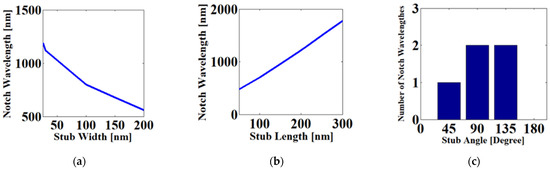
Figure 1.
The relationship between the stub dimensions and the notch wavelength (a) stub width, (b) stub length, and (c) stub rotation angle.
2.1. Structure of Multi-Channel Bandpass Filter (Fixed & Tunable)
The proposed multi-channel bandpass filter consists of a MIM-WG coupled with arrow-shaped cavities, as seen in Figure 2. The up and down arrows are separated by a coupling distance “D”. A parametric analysis has been used to identify the optimum values of the filter geometry to obtain a high transmission efficiency (see Table 1).
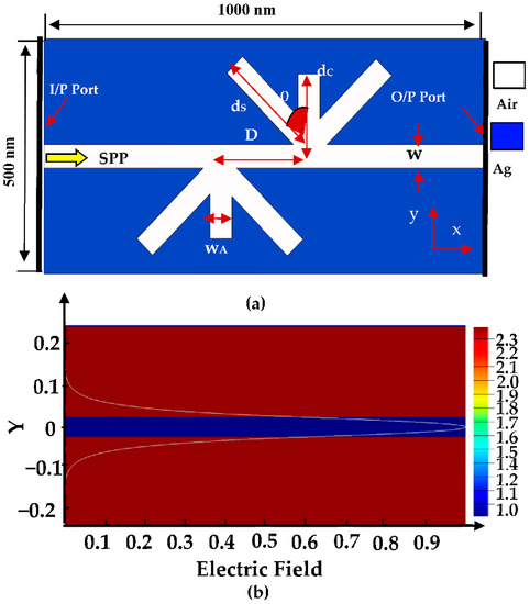
Figure 2.
(a) Schematic diagram of the proposed plasmonic multi-channel bandpass filter structure with geometrical parameters found in Table 1; (b) Incident TM-mode field distribution with λ = 600 nm.

Table 1.
Dimensions of the proposed plasmonic multi-channel bandpass filter (up and down arrows are identical in geometry size).
2.2. Materials
As shown in Figure 2:
- Fixed channels bandpass filter materials are air (insulator medium fills the bus waveguide and dual arrow-shaped cavities) and silver (Ag metal medium). Silver has been selected because it is a dominant conductor in the optical and near-infrared range. The silver permittivity must be determined when studying the filter wavelength response over the desired band. Many analytical models are used to represent the optical properties of the metallic nanoparticles. However, all these models were developed to fit the experimental data (Johnson and Christy). However, the number of parameters, which are used for fitting the experimental data, can affect the accuracy of the simulation results [56,57]. Since there are no reliable models for nanomaterials, the measurements by Johnson and Christy are preferable for expressing silver permittivity (εm) in the visible range [56,58].
- Tunable channels bandpass filter materials are: non-linear optical (NLO) material [59] and silver. The refractive index of NLO materials is sensitive to the intensity of the incident light, which is why the resonance wavelengths can be controlled without changing the outer size of the structure. InGaAsP is one of the top-tier NLO materials because of its chemical stability, high optical damage threshold, ease of attainment in crystalline form, broad operating ranges of wavelength and temperature, and conversion efficiency [60]. InGaAsP fills the bus waveguide and dual arrow-shaped cavities. The equation of nonlinear dielectric constant, εd, for InGaAsP is as follows [40]:where εL is the linear dielectric constant, which is adjusted at 2.25; χ(3) denotes third-order nonlinear susceptibility which reads 4 × 10⁻¹⁸ m2/V2; and |E|2 is the intensity of the incident light that changes the properties of InGaAsP. According to Equation (1), the permittivity of InGaAsP has been modified locally to be 2.65 and 3.05 when changing the incident light intensity from 1017 v2/m2 to 2 × 10¹⁷ v2/m2, respectively. Infrared wavelength LED and laser diode at λ ~ 1.3 μm can be used to illuminate the NLO material (InGaAsP) [61].εd = εL + χ(3) |E|2
2.3. Numerical Method
A two-dimensional finite element method (2D FEM) [62,63,64] (COMSOL Multiphysics Version 5.5) is used to calculate the propagation properties of the depicted structure in Figure 2. Two-dimensional model (2D) is selected rather than three dimensional (3D) model since both models will obtain the same simulation results; on top of that, it is simpler and requires fewer computing resources [65]. However, to ensure that the filter performance is going well with the simulation results, the Ag metal thickness in the z direction is much longer than in the x and y directions [66]. Inspired by [67], the thickness of the metal layer (Ag) in our design is preferred to be more than 15% of the working wavelength. TM-polarized incident light is used to excite the SPP mode at the input port, as seen in Figure 2b. To achieve numerical convergence, the variations of the normalized transmitted power have been studied for three different wavelengths (λ = 540 nm, 760 nm, and 860 nm) with different mesh sizes. Table 2 shows the statistics of that study. So, for numerical convergence, this structure must be discretized in the x and y directions using:
Table 2.
Statistics of mesh size.
- A quadratic shape function.
- “Extremely fine” mesh element size with the total number of elements = 526.
3. Numerical Results
3.1. Fixed Multi-Channel Bandpass Filter
Figure 3 shows the transmission spectra of the proposed filter with a different coupling distance “D” between the double arrow shape. The value of “D” controls the constructive/destructive interference of waves between the arrow resonators and the bus waveguide [68]. This interference between waves must be in phases to cause transmission peaks. We also observed that as the coupling distance continues to rise, multiple discrete transmission bands interfered, causing a broadening in its bandwidth. Table 3 summarizes the filter characteristics with the different values of the coupling distance.
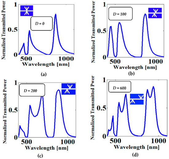
Figure 3.
Transmission spectra with different coupling distance between two plasmonic arrows: (a) D = 0 nm, (b) D = 100 nm, (c) D = 200 nm, and (d) D = 600 nm.
Table 3.
Filter characteristics with various coupling distances between two arrow resonators (values extracted from Figure 3).
3.2. Tunable Multi-Channel Bandpass Filter Based InGaAsP
As shown in Figure 4a, a red shift in the transmission wavelengths occurs as the incident light intensity is increased. Figure 4b clarifies the direct positive relationship between the transmission wavelengths and the illuminated light intensity. Table 4 summarizes the filter transmission characteristics through three light intensities. Based on the previous results, we can shift all of the transmission wavelengths by changing the light intensity. Figure 5 displays the field distribution of the Hz component through two values of the light intensity.
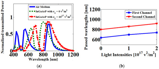
Figure 4.
(a) Transmission spectra with different dielectric mediums; (b) Relation between the light intensity exposed to the NLO (InGaAsP) and the resonance wavelengths.
Table 4.
Filter transmission characteristics through the variation in light intensity exposed to InGaAsP.
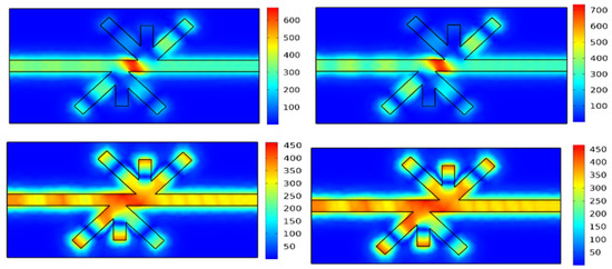
Figure 5.
Magnetic field Hz distribution with different light intensities exposed to non-linear dielectric material (InGaAsP): (a) light intensity e0 = 0 (v2/m2), (b) light intensity e0 = 1017 (v2/m2).
4. Discussion
From the above results:
- A triple-channel bandpass filter with a high transmission efficiency and narrow bandwidth can be designed by selecting the value of the coupling distance to be 100 nm.
- A triple-channel bandpass filter with a high transmission efficiency and wide bandwidth, can be designed by selecting the value of the coupling distance to be more than 200 nm.
- A tunable multi-channel bandpass filter with high transmission peaks can be controlled over a range from 600 nm to 1200, thanks to InGaAsP.
We compare the characteristics of the proposed tunable multi-channel bandpass filter with other previous work, as seen in Table 5. According to this table, the proposed multi-channel bandpass filter has the highest number of passed channels and the highest power efficiency (two of them reach 85%). This tunable multi-channel bandpass filter can work as a wavelength division multiplexing (WDM) device due to its compact size and simple construction.
Table 5.
Comparison between the proposed tunable multichannel bandpass filter and previous works.
The fabrication process of the proposed structure with minimum dimensions of 50 nm is the next challenge. The oblique angle shadow evaporation technique has numerous uses in optical trapping (filtering), surface-enhanced spectroscopy, and sensing, so it can be used to fabricate structures similar to the proposed multi-channel bandpass filter [71], by suspending the mask above the substrate and adjusting the deposition angle to be oblique to the normal surface. The fabrication tolerances must be taken into the account since the geometry of the nano-scaled plasmonic waveguide is insensitive to fabrication errors [72]. The fabrication tolerance of the proposed tunable multi-channel bandpass filter was tested by changing the value of the angle “θ “and the sharp edges. All the sharp edges are slightly curved by radius “R” to be easy for fabrication, as seen in Figure 6a. The variation in the first factor “θ “on the performance of the proposed filter is shown in Figure 6b. It has been observed that any angle deviation within the range of ±2o will have little impact on the filter transmission efficiency, which demonstrates good tolerance and stability. The second impact factor “R”, which affects the performance of the proposed filter, is shown in Figure 6c. It is observed that the edges with radius R < 4 nm have a slightly blue shift in the transmitted wavelengths. This blue shift can be ignored to achieve a simple fabrication process for the proposed filter. Additionally, the variation in the pump light field distribution has been considered a third fabrication tolerance factor, because it may lead to a non-homogeneous tuning of the index distribution within the structure of the waveguide. Therefore, the transmission spectrum has been recalculated while the light intensities of the vertical stub resonators (up/down) and bus waveguide are different from those of the slanted stub resonators (left/right, up/down), as seen in Figure 6d. It has been observed that a blue shift (tiny shift of 30 nm) in the resonance wavelengths happens when the index of the nonlinear material has two different intensities of the pumping light at the same time within the structure. Since the average difference between the resonance wavelengths for a homogeneous and nonhomogeneous pump light field distribution is only 4%, this will not affect the performance and it is relatively acceptable.
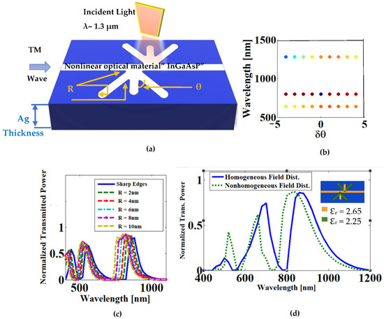
Figure 6.
Fabrication tolerance due to the variation in angle “θ”, the radius of the curved edge “R”, and the pump light field distribution. (a) 3D sketch model for the proposed tunable multi-channel ban-pass filter; (b) variation in angle “θ” Note: Every line (light intensity e0) corresponds to one of the three passing wavelength channels, and the colored dots for each line indicate the variations in transmission efficiency values; (c) transmission spectrum with different curved edges “R”; (d) the variation in the pump light field distribution within the structure of the waveguide. Inset: the different refractive indices of the NLO material due to the non-homogenous pump light field distribution.
5. Conclusions
This study produces a new shape of the multi-channel plasmonic bandpass filter. This filter consists of up and down arrow-shaped cavities coupled with an MIM waveguide. The multichannel bandpass filter provides three passed channels with a good Q-factor and power efficiency. These cavities are filled with a nonlinear optical material (InGaAsP) with a minimum width of 50 nm. The refractive index of the InGaAsP material is sensitive to the intensity of the incident light, which is why the resonance wavelengths can be controlled without changing the outer size of the structure. These light intensities tuned the wavelengths over the range from 600 nm to 1200 nm. The suggested filter demonstrates a good tolerance and stability for the angle deviations within the range of ±2°. Additionally, to obtain a friendly fabrication process for the proposed filter, all the sharp edges can be slightly curved within a radius value of 4 nm. The designed tunable multi-channel bandpass filter can play a role in WDM photonic systems which operate in the visible and near-IR band.
Author Contributions
Conceptualization, S.A.-E., N.F.F.A., H.A.E.-M. and S.S.A.O.; Methodology, S.A.-E., N.F.F.A., H.A.E.-M. and S.S.A.O.; Software, S.A.-E.; validation, S.A.-E., N.F.F.A., H.A.E.-M. and S.S.A.O.; Formal analysis, S.A.-E., N.F.F.A., H.A.E.-M. and S.S.A.O.; Investigation, S.A.-E., N.F.F.A., H.A.E.-M. and S.S.A.O.; Resources, S.S.A.O.; Data curation, S.A.-E. and N.F.F.A.; Writing—original draft preparation, S.A.-E.; Writing—review and editing, S.A.-E., N.F.F.A., H.A.E.-M. and S.S.A.O.; Visualization, S.A.-E.; Supervision, S.A.-E., N.F.F.A., H.A.E.-M. and S.S.A.O.; Project administration, S.A.-E., N.F.F.A., H.A.E.-M. and S.S.A.O. All authors have read and agreed to the published version of the manuscript.
Funding
This research received no external funding.
Data Availability Statement
Not applicable.
Conflicts of Interest
The authors declare no conflict of interest.
References
- Raether, H. Surface plasmons on gratings. In Surface Plasmons on Smooth and Rough Surfaces and on Gratings; Springer: Berlin/Heidelberg, Germany, 1988; pp. 91–116. [Google Scholar]
- Heikal, A.; Hameed, M.F.O.; Obayya, S.S.A. Basic principles of surface plasmon resonance. In Computational Photonic Sensors; Springer: Berlin/Heidelberg, Germany, 2019; pp. 53–72. [Google Scholar]
- Alagdar, M.; Yousif, B.; Areed, N.F.F.; Elzalabani, M. Highly sensitive fiber optic surface plasmon resonance sensor employing 2D nanomaterials. Appl. Phys. A 2020, 126, 522. [Google Scholar] [CrossRef]
- Ummethala, S.; Harter, T.; Koehnle, K.; Li, Z.; Muehlbrandt, S.; Kutuvantavida, Y.; Kemal, J.; Marin-Palomo, P.; Schaefer, J.; Tessmann, A. THz-to-optical conversion in wireless communications using an ultra-broadband plasmonic modulator. Nat. Photonics 2019, 13, 519–524. [Google Scholar] [CrossRef]
- Khani, S.; Danaie, M.; Rezaei, P. Hybrid all-optical infrared metal-insulator-metal plasmonic switch incorporating photonic crystal bandgap structures. Photonics 2020, 40, 100802. [Google Scholar] [CrossRef]
- Peale, R.; Figueiredo, P.; Phelps, J.R.; Chan, K.C.; Abdolvand, R.; Smith, E.M.; Vangala, S. Infrared surface-plasmon-resonance attenuator for broadly controllable effective radiant temperature. Infrared Phys. Technol. 2022, 125, 104253. [Google Scholar] [CrossRef]
- Abd-Elkader, A.E.-S.; Hameed, M.F.O.; Areed, N.F.F.; Mostafa, H.E.-D.; Obayya, S.S.A. Ultracompact AZO-based TE-pass and TM-pass hybrid plasmonic polarizers. JOSA B 2019, 36, 652–661. [Google Scholar] [CrossRef]
- Areed, N.F.F.; El Malt, S.M.; Obayya, S.S.A. Broadband omnidirectional nearly perfect plasmonic absorber for solar energy harvesting. IEEE Photonics J. 2016, 8, 1–18. [Google Scholar] [CrossRef]
- Elrabiaey, M.A.; Areed, N.F.; Obayya, S.S.A. Plasmonic Optical Binary Storage Based on Nematic Liquid Crystal Layers. In Proceedings of the Proc. of PIER, Prague, Czech Republic, 6–9 July 2015; p. 336. [Google Scholar]
- Wu, C.; Guo, Z.; Chen, S.; Yang, J.; Wen, K. Refractive index sensing based on multiple Fano resonances in a plasmonic defective ring-cavity system. Results Phys. 2021, 27, 104508. [Google Scholar] [CrossRef]
- Nurmohammadi, T.; Abbasian, K.; Yadipour, R. Numerical study of dumbbell-shaped gold nanoparticles using in plasmonic waveguides in near infra-red spectrums. Opt. Quantum Electron. 2018, 50, 188. [Google Scholar] [CrossRef]
- Azzam, S.I.; Areed, N.F.; Abd-Elrazzak, M.M.; El-Mikati, H.; Obayya, S.S. Novel symmetric hierarchical mixed finite element analysis for nanophotonic devices. In Proceedings of the 2014 31st National Radio Science Conference (NRSC), Cairo, Egypt, 28–30 April 2014; pp. 341–348. [Google Scholar]
- Islam, M.; Chowdhury, D.R.; Ahmad, A.; Kumar, G. Terahertz plasmonic waveguide based thin film sensor. J. Lightwave Technol. 2017, 35, 5215–5221. [Google Scholar] [CrossRef]
- Lu, L.; Li, F.; Xu, M.; Wang, T.; Wu, J.; Zhou, L.; Su, Y. Mode-selective hybrid plasmonic Bragg grating reflector. IEEE Photonics Technol. Lett. 2012, 24, 1765–1767. [Google Scholar] [CrossRef]
- Zhou, T.; Yang, X.; Chen, M.; Cheng, H.; Guo, Y.; Xie, Y.; Zhang, S.; Xu, J.; Liang, Z. Bragg gratings composed of hollow hybrid plasmonic waveguides with low loss. In Proceedings of the Optoelectronic Devices and Integration IX, SPIE/COS PHOTONICS ASIA, Online, 11–16 October 2020; Volume 11547, p. 1154710. [Google Scholar]
- Du, C.-H.; Chiou, Y.-P. Vertical directional couplers with ultra-short coupling length based on hybrid plasmonic waveguides. J. Lightwave Technol. 2014, 32, 2065–2071. [Google Scholar]
- Park, J.; Kim, K.-Y.; Lee, I.-M.; Na, H.; Lee, S.-Y.; Lee, B. Trapping light in plasmonic waveguides. Opt. Express 2010, 18, 598–623. [Google Scholar] [CrossRef] [PubMed]
- Ebadi, S.M.; Örtegren, J.; Bayati, M.S.; Ram, S.B. A Multipurpose and Highly-Compact Plasmonic Filter Based on Metal-Insulator-Metal Waveguides. IEEE Photonics J. 2020, 12, 4800309. [Google Scholar] [CrossRef]
- Khani, S.; Danaie, M.; Rezaei, P. Plasmonic all-optical metal–insulator–metal switches based on silver nano-rods, comprehensive theoretical analysis and design guidelines. J. Comput. Electron. 2021, 20, 442–457. [Google Scholar] [CrossRef]
- Paul, S.; Ray, M. Multispectral switching using Fano resonance and plasmon-induced transparency in a plasmonic waveguide-coupled resonator system. Plasmonics 2019, 14, 1113–1122. [Google Scholar] [CrossRef]
- Khani, S.; Hayati, M. An ultra-high sensitive plasmonic refractive index sensor using an elliptical resonator and MIM waveguide. Superlattices Microstruct. 2021, 156, 106970. [Google Scholar] [CrossRef]
- Jia, Y.; Song, C.; Liao, Y.; Cai, H. Broadband and Wide-Angle Performance of a Perfect Absorber Using a MIM Structure with 2D MXene. Electronics 2022, 11, 1370. [Google Scholar] [CrossRef]
- Li, Z.; Wang, Y.; Li, T.; Huang, C.; Zhang, Y. Composite optical interference in non-unitary and unitary beam-splitter systems. J. Opt. 2021, 50, 495–501. [Google Scholar] [CrossRef]
- Zegaar, I.; Hocini, A.; Harhouz, A.; Khedrouche, D.; Salah, H.B. Design of a Double-Mode Plasmonic Wavelength Filter Using a Defective Circular Nano-Disk Resonator Coupled to Two MIM Waveguides. Prog. Electromagn. Res. Lett. 2022, 104, 67–75. [Google Scholar] [CrossRef]
- Hasan, M.; Mayoa, F.; Hossain, M.S.; Ahmed, R.; Hossain, M.; Ali, K.; Islam, S. Plasmonic corrugated waveguide coupled to a rectangular nano-resonator as an optical filter. OSA Contin. 2020, 3, 3314–3323. [Google Scholar] [CrossRef]
- Negahdari, R.; Rafiee, E.; Emami, F. Design and simulation of a novel nano-plasmonic split-ring resonator filter. J. Electromagn. Waves 2018, 32, 1925–1938. [Google Scholar] [CrossRef]
- Zhuang, T.; Li, S.; Song, G.; Jiang, P.; Yu, L. Tunable band-stop plasmonic waveguide filter with single-sided multiple-teeth-shaped structure. Phys. Scr. 2019, 94, 095602. [Google Scholar] [CrossRef]
- Shafagh, S.G.; Kaatuzian, H.; Danaie, M. Analysis, design and simulation of MIM plasmonic filters with different geometries for technical parameters improvement. Commun. Theor. Phys. 2020, 72, 085502. [Google Scholar] [CrossRef]
- Khatab, H.M.; Areed, N.F.F.; El-Mikati, H.A.; Hameed, M.F.O.; Obayya, S.S.A. Efficient plasmonic line-up filter for sensing applications. Opt. Quantum Electron. 2021, 54, 47. [Google Scholar] [CrossRef]
- Khani, S.; Danaie, M.; Rezaei, P. Realization of single-mode plasmonic bandpass filters using improved nanodisk resonators. Opt. Commun. 2018, 420, 147–156. [Google Scholar] [CrossRef]
- Dai, J.; Wang, S.; Song, G.; Yu, L.; Wang, L.; Xiao, J. Plasmon-enhanced polarization-selective filter based on multiple holes array filled with nonlinear medium. Mod. Phys. Lett. B 2014, 28, 1450130. [Google Scholar] [CrossRef]
- Qi, Y.; Zhou, P.; Zhang, T.; Zhang, X.; Wang, Y.; Liu, C.; Bai, Y.; Wang, X. Theoretical study of a multichannel plasmonic waveguide notch filter with double-sided nanodisk and two slot cavities. Results Phys. 2019, 14, 102506. [Google Scholar] [CrossRef]
- Zhou, C.; Huo, Y.; Guo, Y.; Niu, Q. Tunable multiple fano resonances and stable plasmonic band-stop filter based on a metal-insulator-metal waveguide. Plasmonics 2021, 16, 1735–1743. [Google Scholar] [CrossRef]
- Zhou, D.; Wang, X.; Zhu, H.; Shen, F. Graphene-based tunable multichannel filter with arithmetic sequence quasiperiodic structure. Optik 2018, 174, 282–288. [Google Scholar] [CrossRef]
- Li, G.; De Sterke, C.M.; Palomba, S. Fundamental limitations to the ultimate Kerr nonlinear performance of plasmonic waveguides. ACS Photonics 2018, 5, 1034–1040. [Google Scholar] [CrossRef]
- Li, G.; de Sterke, C.M.; Palomba, S. Figure of merit for Kerr nonlinear plasmonic waveguides. Laser Photonics Rev. 2016, 10, 639–646. [Google Scholar] [CrossRef]
- Nasari, H.; Abrishamian, M.S. All-optical tunable notch filter by use of Kerr nonlinearity in the graphene microribbon array. JOSA B 2014, 31, 1691–1697. [Google Scholar] [CrossRef]
- Li, J.; Tao, J.; Chen, Z.H.; Huang, X.G. All-optical controlling based on nonlinear graphene plasmonic waveguides. Opt. Express 2016, 24, 22169–22176. [Google Scholar] [CrossRef] [PubMed]
- Heydari, M.B.; Samiei, M.H.V. A short review on graphene-based filters: Perspectives and challenges. arXiv 2020, arXiv:07176. [Google Scholar]
- Kamari, M.; Hayati, M.; Khosravi, S. Tunable infrared wide band-stop plasmonic filter using T-shaped resonators. Mater. Sci. Semicond. Process. 2021, 133, 105983. [Google Scholar] [CrossRef]
- Yin, S.; Liu, Y.J.; Xiao, D.; He, H.; Luo, D.; Jiang, S.; Dai, H.; Ji, W.; Sun, X.W. Liquid-crystal-based tunable plasmonic waveguide filters. J. Phys. D Appl. Phys. 2018, 51, 235101. [Google Scholar] [CrossRef]
- Arianfard, H.; Khajeheian, B.; Ghayour, R. Tunable band (pass and stop) filters based on plasmonic structures using Kerr-type nonlinear rectangular nanocavity. Opt. Eng. 2016, 56, 121902. [Google Scholar] [CrossRef]
- Zhang, Z.; Shi, F.; Chen, Y. Tunable Multichannel Plasmonic Filter Based on Coupling-Induced Mode Splitting. Plasmonics 2015, 10, 139–144. [Google Scholar] [CrossRef]
- Xu, H.; Xiao, G.; Xiao, W.; Chen, Q. Tunable multimode plasmonic filter based on asymmetric dual side-coupled U-shape cavities resonators. Optik 2019, 182, 324–330. [Google Scholar] [CrossRef]
- Mittapalli, V.; Khan, H. Excitation schemes of plasmonic angular ring resonator-based band-pass filters using a MIM waveguide. Photonics 2019, 6, 41. [Google Scholar] [CrossRef]
- Khani, S.; Danaie, M.; Rezaei, P. Design of a single-mode plasmonic bandpass filter using a hexagonal resonator coupled to graded-stub waveguides. Plasmonics 2019, 14, 53–62. [Google Scholar] [CrossRef]
- Lee, J.; Kim, M.; Park, H.-K.; Kim, I.Y. Motion artifact reduction in wearable photoplethysmography based on multi-channel sensors with multiple wavelengths. Sensors 2020, 20, 1493. [Google Scholar] [CrossRef] [PubMed]
- Zha, S.; Zhang, H.; Sun, C.; Feng, Y.; Lu, J. Multi-Wavelength filters of templated blue phase liquid crystal. Crystals 2019, 9, 451. [Google Scholar] [CrossRef]
- Liao, R.; Tian, H.; Liu, W.; Li, R.; Song, Y.; Hu, M. Dual-comb generation from a single laser source: Principles and spectroscopic applications towards mid-IR—A review. J. Phys. Photonics 2020, 2, 042006. [Google Scholar] [CrossRef]
- Teğin, U.; Rahmani, B.; Kakkava, E.; Psaltis, D.; Moser, C. All-fiber spatiotemporally mode-locked laser with multimode fiber-based filtering. Opt. Express 2020, 28, 23433–23438. [Google Scholar] [CrossRef]
- Shapiro, E.G.e.; Shapiro, D.A. Suppression of nonlinear distortion in a high-speed multichannel communication line with variable quadratic dispersion compensation. Quantum Electron. 2021, 51, 635. [Google Scholar] [CrossRef]
- Rafiee, E.; Negahdari, R.; Emami, F. Plasmonic multi channel filter based on split ring resonators: Application to photothermal therapy. Photonics Nanostructures-Fundam. Appl. 2019, 33, 21–28. [Google Scholar] [CrossRef]
- Fallahi, V.; Seifouri, M.; Mohammadi, M. A new design of optical add/drop filters and multi-channel filters based on hexagonal PhCRR for WDM systems. Photonic Netw. Commun. 2019, 37, 100–109. [Google Scholar] [CrossRef]
- Sharma, N.; Singh, H.; Singh, P. Mitigation of FWM in the Fiber Optic DWDM System by using Different Modulation Techniques and Optical Filters. In Proceedings of the 2020 5th International Conference on Communication and Electronics Systems (ICCES), Coimbatore, India, 10–12 June 2020; pp. 343–348. [Google Scholar]
- Yu, J.; Li, X.; Zhou, W. Tutorial: Broadband fiber-wireless integration for 5G+ communication. Apl. Photonics 2018, 3, 111101. [Google Scholar] [CrossRef]
- Barchiesi, D.; Grosges, T. Fitting the optical constants of gold, silver, chromium, titanium, and aluminum in the visible bandwidth. J. Nanophotonics 2014, 8, 083097. [Google Scholar] [CrossRef]
- Hao, F.; Nordlander, P. Efficient dielectric function for FDTD simulation of the optical properties of silver and gold nanoparticles. Chem. Phys. Lett. 2007, 446, 115–118. [Google Scholar] [CrossRef]
- Johnson, P.B.; Christy, R.-W. Optical constants of the noble metals. Phys. Rev. B 1972, 6, 4370. [Google Scholar] [CrossRef]
- Kauranen, M.; Zayats, A.V. Nonlinear plasmonics. Nat. Photonics 2012, 6, 737–748. [Google Scholar] [CrossRef]
- Arivuoli, D. Fundamentals of nonlinear optical materials. Pramana 2001, 57, 871–883. [Google Scholar] [CrossRef]
- Yamazoe, Y.; Nishino, T.; Hamakawa, Y.; Kariya, T. Bandgap Energy of InGaAsP Quaternary Alloy. Jpn. J. Appl. Phys. 1980, 19, 1473–1479. [Google Scholar] [CrossRef]
- Rajarajan, M.; Obayya, S.S.A.; Rahman, B.A.; Grattan, K.T.; El-Mikati, H.A. Design of compact optical bends with a trench by use of finite-element and beam-propagation methods. Appl. Opt. 2000, 39, 4946–4953. [Google Scholar] [CrossRef]
- Zienkiewicz, O.C.; Taylor, R.L.; Zhu, J.Z. The Finite Element Method: Its Basis and Fundamentals; Elsevier: Amsterdam, The Netherlands, 2005. [Google Scholar]
- Anwar, N.; Obayya, S.S.A.; Haxha, S.; Themistos, C.; Rahman, B.; Grattan, K.T. The effect of fabrication parameters on a ridge Mach-Zender interferometric (MZI) modulator. J. Lightwave Technol. 2002, 20, 854–861. [Google Scholar] [CrossRef]
- Chou Chau, Y.-F.; Chou Chao, C.-T.; Huang, H.J.; Kooh, M.R.R.; Kumara, N.T.R.N.; Lim, C.M.; Chiang, H.-P. Ultrawide Bandgap and High Sensitivity of a Plasmonic Metal-Insulator-Metal Waveguide Filter with Cavity and Baffles. Nanomaterials 2020, 10, 2030. [Google Scholar] [CrossRef]
- Han, Z.; He, S. Two-dimensional model for three-dimensional index-guided multimode plasmonic waveguides and the design of ultrasmall multimode interference splitters. Appl. Opt. 2007, 46, 6223–6227. [Google Scholar] [CrossRef] [PubMed]
- Shibayama, J.; Kawai, H.; Yamauchi, J.; Nakano, H. Analysis of a 3D MIM waveguide-based plasmonic demultiplexer using the TRC-FDTD method. Opt. Commun. 2019, 452, 360–365. [Google Scholar] [CrossRef]
- Haus, H. Waves and fields in optoelectronics. Prenctice-Hall. Inc. Englewood Cliffs NJ 1984, 7632, 208. [Google Scholar]
- Chen, Z.; Chen, J.; Li, Y.; Qian, J.; Qi, J.; Xu, J.; Sun, Q. Highly efficient narrow-band plasmonic waveguide filter based on cascaded slot cavities. Chin. Opt. Lett. 2013, 11, 112401. [Google Scholar] [CrossRef]
- Lu, H.; Yue, Z.; Zhao, J. Multiple plasmonically induced transparency for chip-scale bandpass filters in metallic nanowaveguides. Opt. Commun. 2018, 414, 16–21. [Google Scholar] [CrossRef]
- Gu, P.; Zhang, W.; Zhang, G. Plasmonic nanogaps: From fabrications to optical applications. Adv. Mater. Interfaces 2018, 5, 1800648. [Google Scholar] [CrossRef]
- Jung, J. Optimal design of plasmonic waveguide with fabrication tolerance. Opt. Commun. 2017, 395, 139–146. [Google Scholar] [CrossRef]
Publisher’s Note: MDPI stays neutral with regard to jurisdictional claims in published maps and institutional affiliations. |
© 2022 by the authors. Licensee MDPI, Basel, Switzerland. This article is an open access article distributed under the terms and conditions of the Creative Commons Attribution (CC BY) license (https://creativecommons.org/licenses/by/4.0/).