Article

Passivation Effect of CsPbI3 Quantum Dots on the Performance and Stability of Perovskite Solar Cells

State Key Laboratory of Electronic Thin Films and Integrated Devices, School of Optoelectronic Science and Engineering, University of Electronic Science and Technology of China (UESTC), Chengdu 610054, China
*
Author to whom correspondence should be addressed.
Photonics 2022, 9(1), 3; https://doi.org/10.3390/photonics9010003
Submission received: 30 November 2021 / Revised: 17 December 2021 / Accepted: 20 December 2021 / Published: 22 December 2021
(This article belongs to the Special Issue Advances in Photovoltaic Technologies from Atomic to Device Scale)

Abstract

:
The quality of active layer film is the key factor affecting the performance of perovskite solar cells. In this work, we incorporated CsPbI3 quantum dots (QDs) materials into the MAPbI3 perovskite precursor to form photoactive layer. On one hand, CsPbI3 QDs can be used as nucleation center to enhance the compactness of the perovskite film, and on the other hand, partially CsPbI3 QDs can be dissociated as anions and cations to passivate vacancy defects in the perovskite active layer. As a result, the film quality of the active layer was improved remarkably, thus exciton recombination was reduced, and carrier transfer increased accordingly. The devices based on doped-CsPbI3 QDs film had higher short circuit current, open circuit voltage and filling factor. Finally, the power conversion efficiency (PCE) was greatly enhanced from 14.85% to 17.04%. Furthermore, optimized devices also exhibited better stability. This work provides an effective strategy for the processing of high-quality perovskite films, which is of great value for the preparation and research of perovskite photoelectronic devices.

1. Introduction

Solar energy has been attracting attention as an important representative of renewable and clean energy, and the development of all kinds of low-cost and high-performance solar cells is of great research significance [1,2,3]. Among them, the new generation of perovskite solar cells (PSCs) have many advantages, such as low cost, long exciton diffusion length, adjustable band gap, etc., which have attracted much attention [4,5,6,7]. In recent years, perovskite solar cells have achieved a breakthrough in power conversion efficiency (PCE) from 3.8% to 25.5%, and are considered as the most promising new solar cells [8,9]. However, it is well known that a large number of defects in polycrystalline perovskite films have an important influence on carrier recombination and ion migration in perovskite solar cells, in which nonradiative recombination is the main means of charge loss, and it largely determines the power conversion efficiency and stability of perovskite solar cells [10,11]. Therefore, optimizing the film forming quality of the perovskite active layer and selecting the appropriate interface passivation strategy to passivate the defects of the perovskite film can improve charge extraction and transport to enhance the performance of the perovskite solar cells significantly [12,13,14]. In this context, Li et al. [15] used 4-ammonium chloride butyl phosphonic acid as the additives in the perovskite precursor solution. Through the strong hydrogen bonds of organic additives and perovskite, the crystallization rate of perovskite film was adjusted. Eventually the PCE increased from 8.8% to 16.7%. However, the passivating material used in the method reported above is based on organic molecules, and for the perovskite host material, the organic molecules may introduce impurity ions, potentially causing impurity defects in the perovskite film. In addition, different chain lengths of organic molecules may lead to spectral shift caused by polarity changes, which will also affect the intrinsic optical properties of perovskites. Therefore, it is of great significance to select suitable passivators to reduce the introduction of irrelevant ions, and optimize the proportion of elements to prepare efficient and stable PSCs.
In recent years, perovskite quantum dots (QDs) materials have attracted much attention due to their excellent photoelectric properties [16,17,18,19]. Perovskite quantum dots and three-dimensional perovskite materials have similar elemental composition, physical and chemical properties and lattice parameters. Therefore, the combination of three-dimensional perovskite materials and perovskite quantum dots has become a research hotspot. Therefore, it is of important research value to use inorganic quantum dot materials to modify the functional layer of perovskite solar cells to improve the performance and stability of perovskite solar cells.
In this work, we introduced CsPbI3 QDs into the precursor solution of PSCs. On the one hand, part of CsPbI3 QDs were used as nucleation center to improve the morphology of the active layer film. On the other hand, the partially disintegrated CsPbI3 QDs were used as the anions and cations to fill the ion vacancy defects in the active layer to improve the film quality in terms of the element proportion and crystallinity of the active layer. Finally, inorganic perovskite QDs were used to regulate the growth of perovskite films to achieve high crystallinity, large grain size and fewer defects. As a result, reduced exciton recombination and improved carrier transfer help to enhance the device efficiency finally. The PCE of the optimized devices reached 17.04%, which is much higher than that of the control devices (14.85%). In addition, optimized devices also exhibit good stability, and the performance decay is much slower than that of conventional standard devices in the same environment.

2. Materials and Methods

Chlorobenzene (CB), anhydrous N, N-dimethylformamide (DMF) were purchased from Sigma-Aldrich. Other materials such as lead iodide (PbI2), methyl ammonium iodide (MAI), poly (3, 4-ethylenedioxythiophene): polybenzenesulfonate (PEDOT: PSS), phenyl-C61-methyl butyrate (PCBM) were purchased from Xi’an Polymer Light Technology Corp. All these materials were used as received.
A cesium source was prepared with 0.163 g Cs2CO3 (Sigma-Aldrich, St. Louis, MO, USA, 99.9%), 8 mL octadecenes (Ode, Tokyo, Japan, 90%, Alfa AESAR) and 0.5 mL oleic acid (OA, 90%, Alfa AESAR) heated in a 100 mL flask at vacuum temperature for two hours. Specifically, the solution was degassed by heating in vacuum for 1 h (90 °C), followed by further heating to 150 °C under N2 until the Cs2CO3 was completely dissolved, and finally cooled under N2 for use. To synthesize CsPbI3 QDs, 0.138 g PbI2 (Sigma-Aldrich), 10 mL ODE (Alfa Aesar, Haverhill, MA, USA) and a volume ratio of 1 were prepared under N2 condition: A mixture of 1 OA and oleic acid amine (Ola, Aladdin) was injected into a 50 mL three-necked flask, degassed in a vacuum at 120 °C to ensure complete dissolution of PbI2, and then heated to 170 °C under N2. Immediately, 1 mL of cesium source solution was injected. After five seconds, the colloid solution was placed in in an ice-water bath to be cooled. At the end of the reaction, the accumulated QDs was separated by centrifugation (10,000× g, 10 min). Finally, CsPbI3 QDs were dispersed in n-octane for later use.
The device structure of perovskite solar cell is shown in Figure 1a, and the cross-sectional image SEM of the device is shown in Figure 1b. PEDOT: PSS, MAPbI3, PCBM and Bphen are selected as the hole transport layer, perovskite photoactive layer, electron transport layer and hole barrier layer of the device. ITO and Ag were used as anode and cathode, respectively. Before the preparation of PEDOT: PSS layer, the 15 Ω/SQ ITO coated glass substrate was continuously washed in an ultrasonic bath with water-detergent solution, acetone solvent, deionized water and isopropanol (IPA) solvent, respectively. The cleaned ITO substrate was placed in an oven and dried at 80 °C, followed by ozone-UV treatment for 20 min. Then, PEDOT: PSS solution was drip-coated on ITO substrate at 3000 rpm for 60 s. After 20 min of hot annealing at 150 °C, the substrate was transferred into the glove box (O2, H2O < 1 ppm). Perovskite precursor solution was prepared by mixing 744 mg MAI and 254.3 mg PbI2 in 1 mL dimethylformamide (DMF). For different control groups, 1 wt%, 2 wt% and 3 wt% CsPbI3 QDs dispersions were added into the precursor solution, respectively. Then, precursor solution was stirred in the glove box for more than 4 h (500 rpm, 40 °C). Drops of 45 µL mixed perovskite precursor solution were spin-coated at 4000 rpm on the ITO/PEDOT:PSS substrate for 25 s. After a delay of 7 s, 200 µL of the chlorobenzene (CB) anti-solvent was dropped and spin-cast onto the precursor film. Afterward, the prepared films were dried at 110 °C for 20 min. The concentration of PCBM solution was 20 mg/mL, the PCBM solution was spin-coated at 3000 rpm on the perovskite film for 40 s, and then annealed at 120 °C for 10 min. The PCBM layer in our experiment is about 60 nm. Subsequently, Bphen was deposited at a rate of 1 Å s−1 under high vacuum conditions. Followed by the deposition of Ag as anode at a deposition speed of 5 Å s−1. The active area of these PSCs was 0.02 cm2.
We used Shimazu UV1700 UV-visible absorption system to measure the UV-visible absorption spectra of CsPbI3 QDs and perovskite films. Scanning electron microscopy (SEM) (FEI Inspect F50) was used to measure the surface morphology of perovskite films. The distribution of the elements was detected by X-ray dispersive X-ray analysis (EDS). The crystal structure was characterized by X-ray diffraction (XRD) (D2 PHASER). Using a time-dependent single photometer system (FL-TCSPC, Horiba Jobin Yvon), stimulated by a 550 nm picosecond pulse laser, photoluminescence spectra (PL) and time-resolved photoluminescence spectra (TRPL) were measured. An AM1.5G solar simulator was used as the light source, and the lighting power is 100 mW/cm2. The current density voltage (J-V) curves of the device under illumination were measured with a Keithley4200 semiconductor analyzer. External quantum efficiency (EQE) curves were obtained using xenon lamps calibrated through a monochromator calibrated by a standard silicon solar cell. All measurements were made at room temperature.

3. Results and Discussion

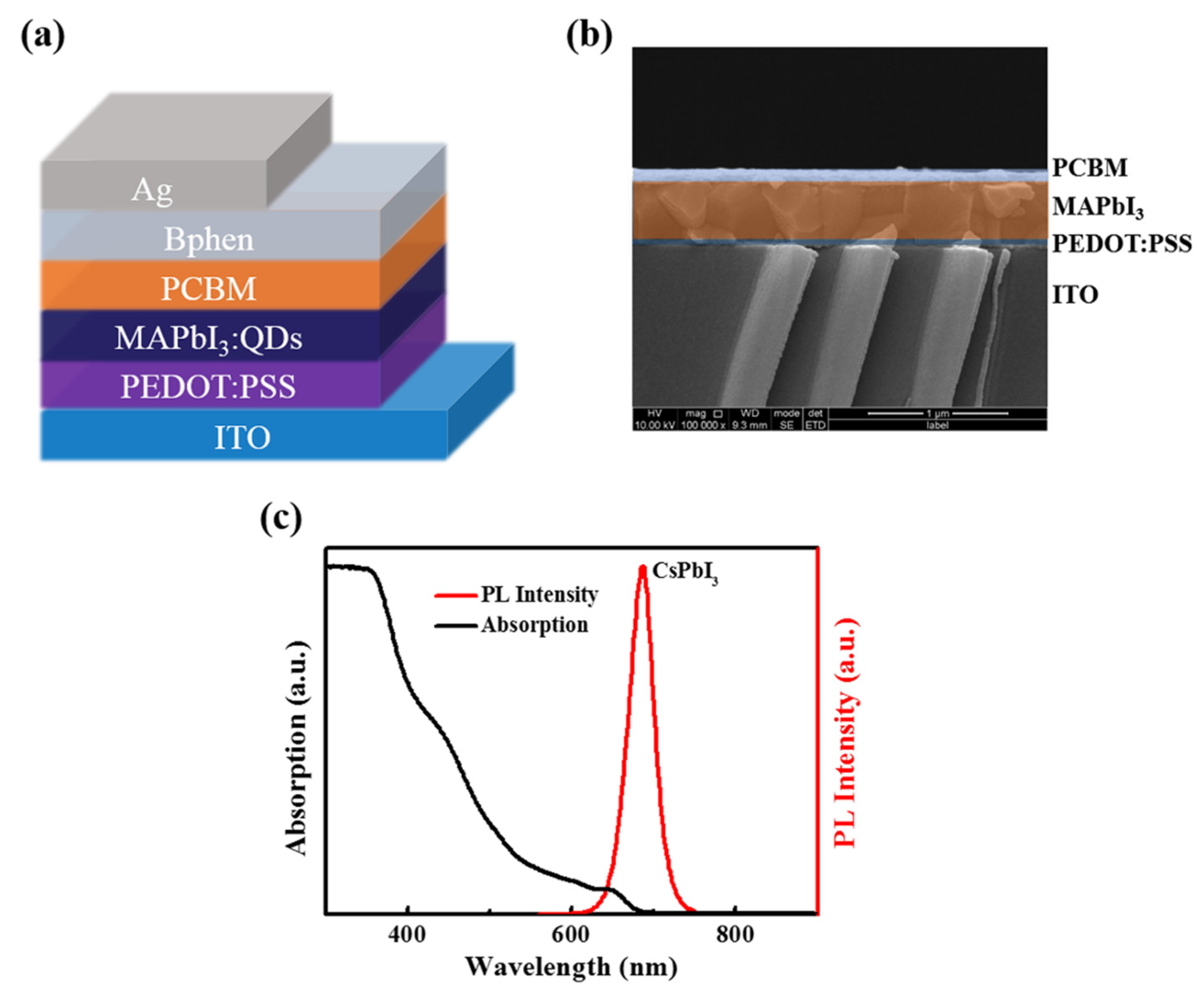
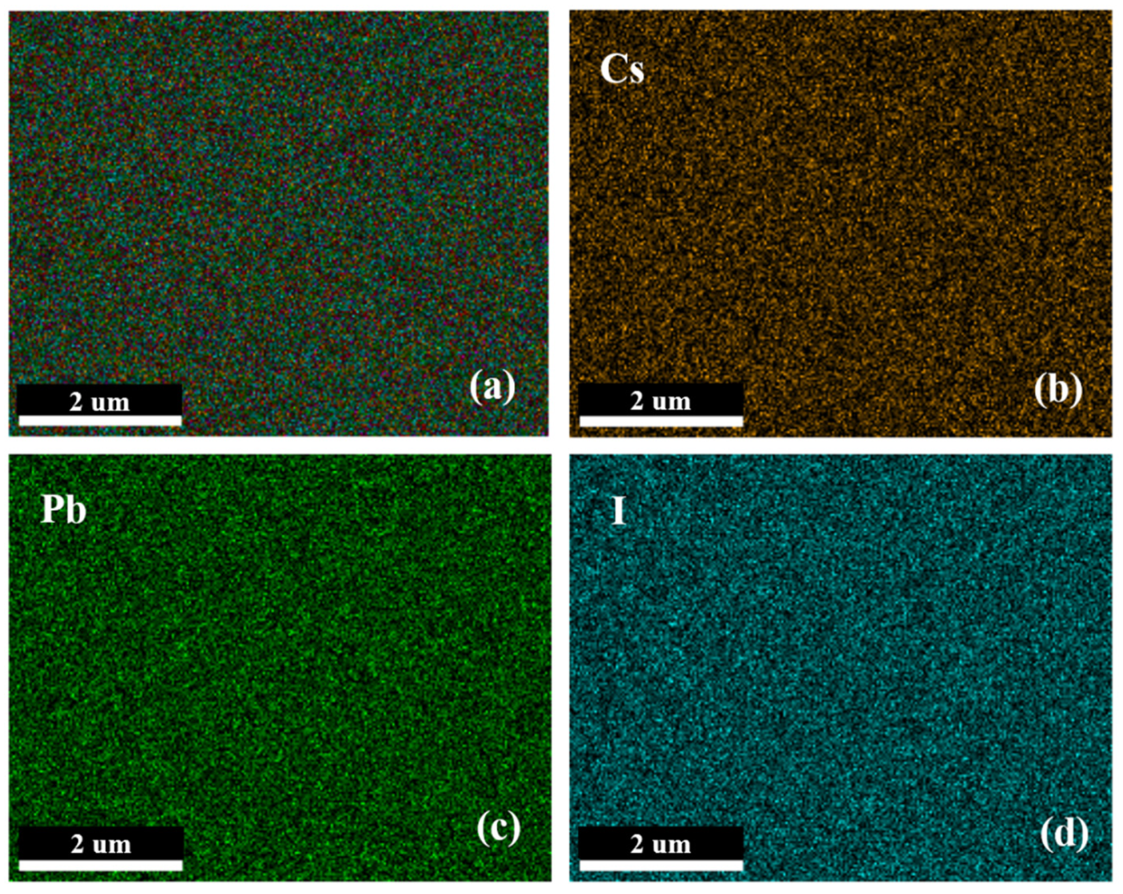
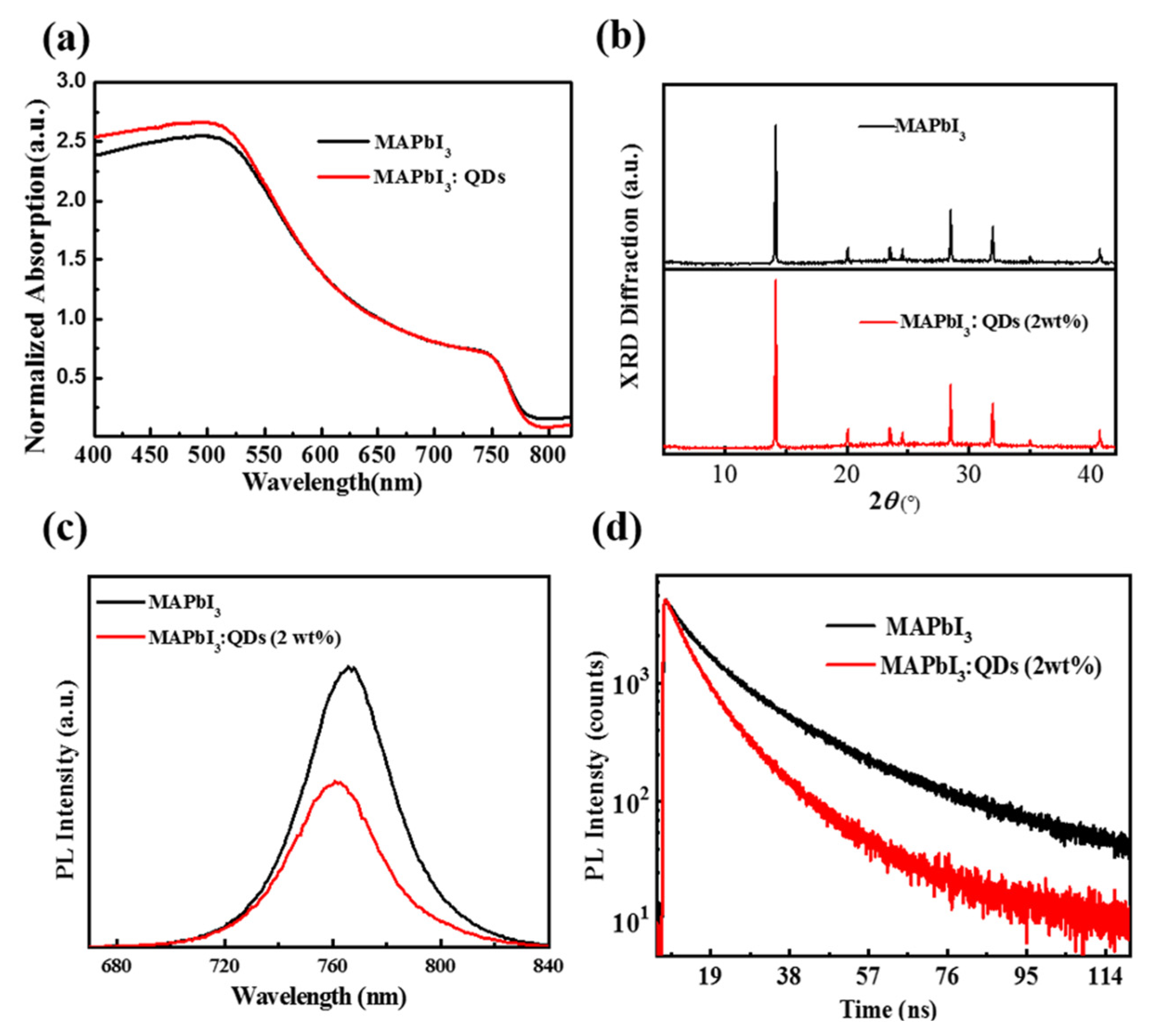
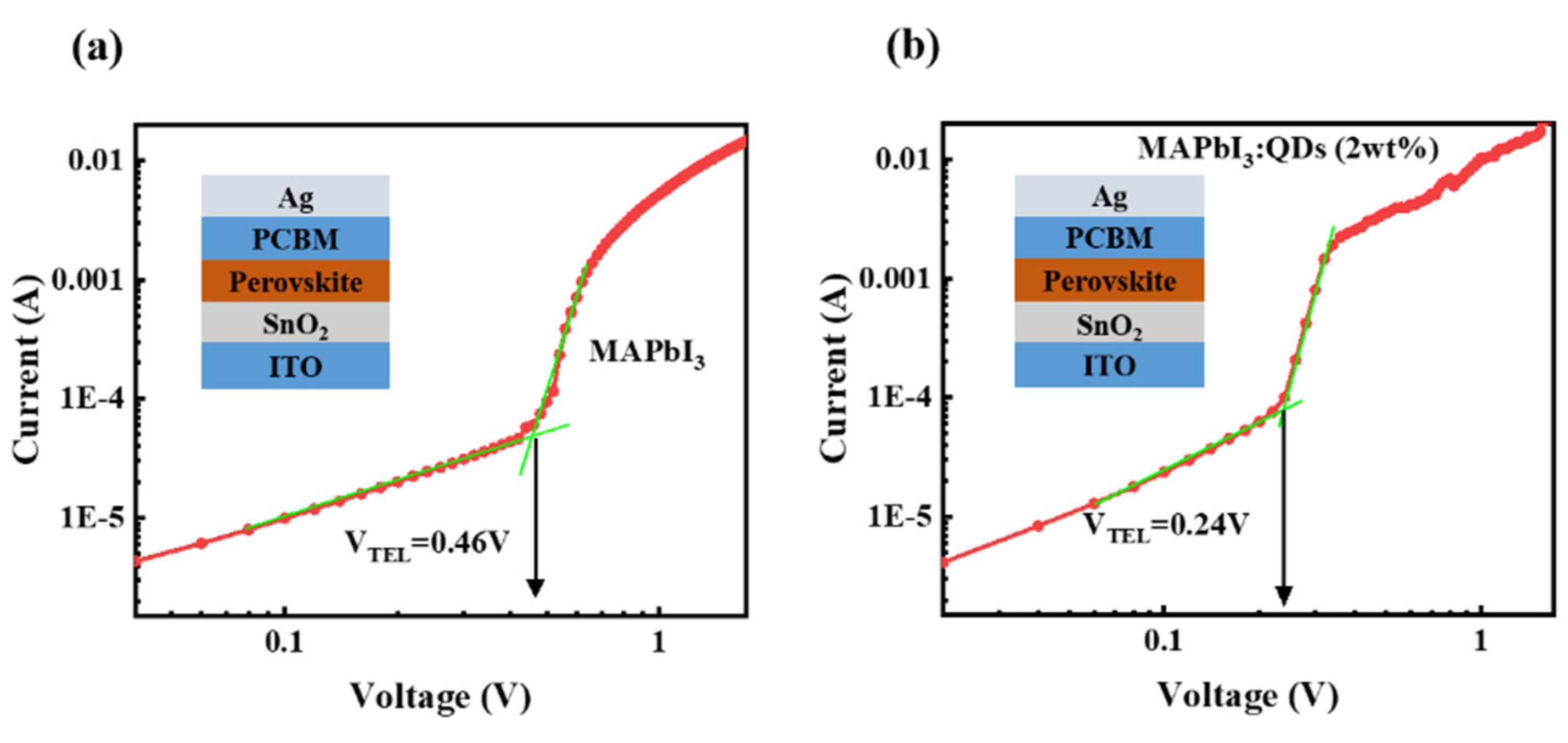
3.1. Characterization and Test

In order to characterize the optical properties of CsPbI3 QDs, we measured the UV-Vis spectrum and steady-state photoluminescence spectrum. As shown in Figure 1a,c, a strong PL emission peak can be observed at 687 nm for CsPbI3 QDs, which is consistent with the absorption and emission wavelength range of CsPbI3 material system reported in literature [20]. It is well known that the photoelectric properties of quantum dot materials are related to their size and purity. We observed that the PL emission peak intensity of CsPbI3 QDs is symmetric, and the width of the half-wave peak is narrow (35 nm), which indicates that the CsPbI3 QDs are high in purity. CsPbI3 QDs with good uniformity are more easily dispersed in the process of mixing the active layer, which would play a homogenized passivation effect on the defects in different positions to ensure the uniformity and flatness of active layer film.
In order to prove that CsPbI3 QDs are uniformly mixed into the perovskite film, we obtained the element distribution image by EDS Mapping, and the test results are shown in Figure 2. As we can see, Cs elements representing the characteristic elements of CsPbI3 QDs were distributed in the whole test area, indicating that CsPbI3 QDs were successfully incorporated into the film of MAPbI3 active layer. In Figure 2b, the intensity distribution of Cs elements in the whole test area has good evenness, indicating that CsPbI3 QDs are evenly distributed in the perovskite active layer, which is conducive to the formation of uniform and stable perovskite film. In addition, the incorporation of Cs element introduces metallic inorganic cations into the active layer of perovskite to achieve the effect of cation passivation, and further improve the morphology of the film.
In order to more directly study the influence of CsPbI3 QDs on the morphology of perovskite films, we tested the surface morphology of perovskite active layer films doped with different proportions of CsPbI3 QDs by SEM. As shown in Figure 3, the surface morphologies of perovskite films doped with different proportions of CsPbI3 QDs are obviously different. The perovskite film without CsPbI3 QDs has small grains and poor crystallinity. With the moderate addition of CsPbI3 QDs, the grain size of perovskite film gradually becomes larger. We have made a quantitative size distribution in Figure 3. For perovskite films doped with 0, 1 wt%, 2 wt%, 3 wt%, their average grain diameter is 247.25 nm, 281.22 nm, 352.87 nm, 274.90 nm respectively. This is because as the nucleation center, CsPbI3 QDs can promote the crystal growth during the perovskite crystallization process and induce the formation of three-dimensional perovskite grains with large size. On the other hand, the doping of CsPbI3 QDs introduces additional metal cationic halogen anions, which not only regulates the element proportion of the active layer, but also passivates some ion vacancy defects and surface grain boundaries, thus improving the film quality of the active layer. However, with excessive incorporation of CsPbI3 QDs, as shown in Figure 3d, the film morphology of the active layer doped with 3% CsPbI3 QDs is not as good as that of the active layer doped with 2% CsPbI3 QDs in Figure 3c. This is because excessive doping will lead to the imbalance of element proportion and affect the crystallinity of perovskite and the film morphology. In general, the active layer of perovskite doped with 2% CsPbI3 QDs has the largest grain size, which can reach nearly micron level. The smooth and dense perovskite film can form a closer interface contact with the transport layer, thus reducing the interface recombination of excitons and improving the extraction efficiency of photogenerated carriers [21]. In addition, the active perovskite layer with large grains is generally characterized by a low grain boundary density, which reduces the density of defect states in the perovskite film and effectively reduces the charge recombination in defects. The experimental results prove that the incorporation of CsPbI3 QDs can improve the morphology of the perovskite active layer, so as to prepare high-quality perovskite films and improve the photovoltaic performance of the devices potentially.
In order to further study the effect of CsPbI3 QDs on the photoelectric properties of perovskite films, the active layer was characterized by spectra and crystallization tests. Figure 4a shows the UV-Vis absorption spectrum of the perovskite film with and without CsPbI3 QDs. It can be seen that the active layer film doped with CsPbI3 QDs has almost the same absorption spectrum and absorption intensity compared with the film without CsPbI3 QDs, both of which only exhibit MAPbI3 characteristic absorption. This indicates that the incorporation of CsPbI3 QDs does not change the light absorption capacity of the active layer. Then, we tested the XRD peak patterns of two kinds of perovskite films. As shown in Figure 4b, the XRD of two films both showed three main intense diffraction peaks at 2θ = 14.4°, 28.8° and 31.8°, which represent the (110), (220), (310) planes, respectively, of the MAPbI3 perovskite crystalline structure [22,23]. This suggests that there is no alloy state of MAxCs1-xPbI3 in the active layer. However, compared with control film, the perovskite film doped with CsPbI3 QDs shows higher and sharper characteristic peaks in all three diffraction angles. The intensity of the diffraction peak corresponds to the crystallinity of the film. In general, the strong XRD diffraction intensity indicates that the crystallinity of this orientation is good, which is conducive to the formation of large and uniform grains [24]. The results of XRD show that the doping of CsPbI3 QDs can enhance the crystallinity of perovskite films and obtain higher quality perovskite films to reduce exciton recombination and enhancing carrier extraction, which is consistent with the results of SEM.
In order to investigate the effect of the introduction of CsPbI3 QDs on the energy transfer and carrier recombination of PSCs, we measured the PL and TRPL spectra of two perovskite films with the test structure of ITO/PEDOT: PSS/perovskite active layers. Figure 4c shows the PL spectra of the two films. Both of them show the characteristic PL spectrum of MAPbI3, which indicates that the introduction of CsPbI3 will not form alloy state of MAxCs1−x PbI3 in the active layer. However, compared with the control device, the PL peak of the CsPbI3 QDs-doped film shows a blue shift from 766 nm to 760 nm, indicating that the surface trap of the active layer is effectively passivated [25]. In addition, compared with the undoped film, the PL peak strength of the doped film shows an obvious quenching phenomenon, which indicates that the doped CsPbI3 QDs is conducive to the extraction of carriers from perovskite films. Figure 4d shows the time-resolved photoluminescence (TRPL) spectrum, which can be used to further study the charge transfer kinetics. According to the TRPL results, the rapid decay lifetime of the perovskite films doped with CsPbI3 QDs is significantly lower than that of the undoped films. Since reduced fast decay lifetimes indicate faster and efficient charge-carrier transfer at the interface, it can be concluded that perovskite doped CsPbI3 QDs has better interfacial properties and charge transfer capacity.
In order to further investigate the effect of CsPbI3 QDs on passivating defects, we estimated the trap-state density of perovskite film by equation [26]:
n t = 2 ε 0 ε r V T E L q L 2
where nt is the trap state density, VTFL is the trap-filled limit voltage, L is the thickness of the perovskite films (400 nm), q is the elementary charge, ε0 is the vacuum permittivity, εr is relative dielectric constant of MAPbI3 (6.5). As showed in Figure 5, the trap-filled limit voltages of 0.46 V and 0.24 V were measured in the electron-only devices. According to the equation, the trap state density of two perovskite films can be calculated to be 2.73 × 10¹⁵ and 1.42 × 1015 cm−3, respectively, indicating that some defects have been passivated by introducing CsPbI3 QDs. The reduced trap density is related to the improved quality of the perovskite film, which is beneficial for device stability and carrier dynamics. It can be mutually confirmed with XRD, PL, and TRPL results.

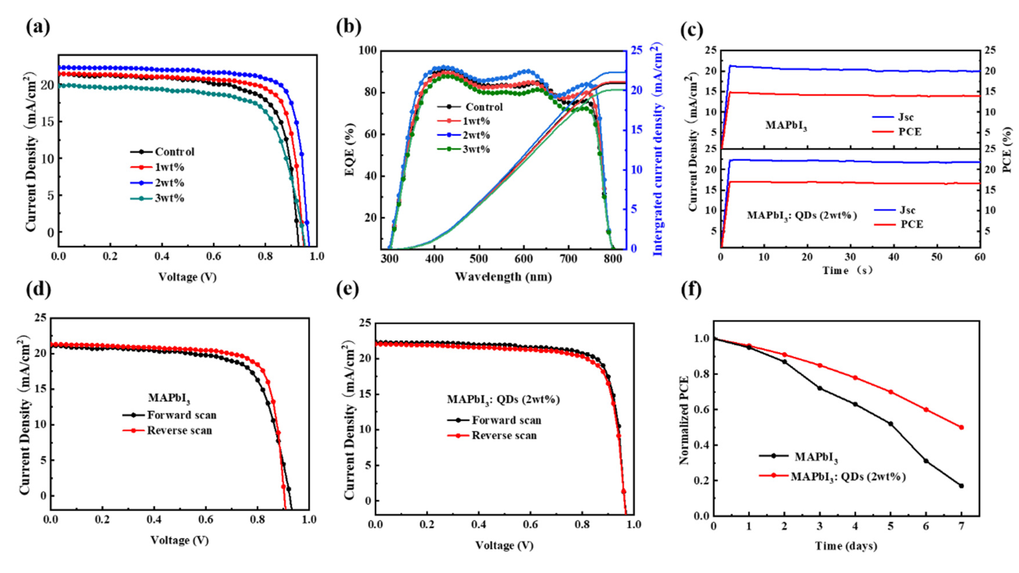
3.2. Performance of PSCs

In order to further study the effect of CsPbI3 QDs on the performance of perovskite devices, we prepared a series of perovskite solar cells using perovskite thin films with different doping ratios of CsPbI3 QDs as the active layer, and tested their photovoltaic performance. Besides, in order to ensure the repeatability of our devices, 20 devices were fabricated and characterized at each ratio. The distribution of their performance parameters is showed in Figure 6. And Table 1 is the average performance statistics of these devices. The results show that CsPbI3 QDs doped in the active layer has a great influence on the performance of PSCs, changing the short-circuit current, open-circuit voltage and filling factor of the devices. The PSCs doped with 2% CsPbI3 QDs showed the best performance, with the short-circuit current, open-circuit voltage, fill factor and energy conversion efficiency reaching 22.27 mA cm−2, 0.961 V, 79.63% and 17.04%, respectively. The short-circuit current, open-circuit voltage and fill factor of PSCs without CsPbI3 QDs are 21.32 mA cm−2, 0.934 V, 74.59% and 14.85%, respectively. In contrast, the doping of CsPbI3 QDs significantly increased short-circuit current, open-circuit voltage, fill factor, resulting in a 15% increase in PCE. The higher performance of the device with CsPbI3 QDs is due to the better quality of the perovskite active layer film, which reduces exciton recombination and improves carrier transfer efficiency, which is consistent with the previous characterization conclusion of the films. The passivated perovskite film also formed the better interface contact with both hole transport layer and electron transport layer, which is conducive to the improvement of open-circuit voltage to improve device performance [27,28].
At the same time, we also showed J-V characteristics and EQE curves of PSCs with different doping ratios of CsPbI3 QDs, and the test results are shown in Figure 7a,b. It can be seen that, within the wavelength range of the response of the device, the EQE curves of the PSCs doped with 2 wt% CsPbI3 QDs is higher than those of other devices, which is consistent with the JSC variation trend of the J-V curve. The value of the integrated current obtained from the EQE curves is approximately the same as the measured current.
Next, we tested the PCE output stability of optimized and control devices. As shown in Figure 7d, we applied a working voltage of 0.85 V to both devices under the simulated sunlight of AM 1.5 g with a light intensity of 100 mW cm−2, and recorded the time function curve of the photocurrent density of PSCs. As can be seen from the Figure 7c, the output peak of current density of both devices reached rapidly after the beginning of illumination. After 60 s continuous illumination, the output value of current density and steady-state PCE of two devices reached 22.15 mA cm2, 16.91% and 21.12 mA cm−2, 14.68%. It is basically consistent with the photocurrent density and PCE value in J-V test. We also compare the hysteresis of the two devices in Figure 7d,e. It can be seen that the hysteresis of the optimized device under forward scanning and reverse scanning is much weaker than that of the control device, which is due to the passivated defects and fewer trap states weaken the hysteresis effectively [29,30].
Finally, we studied the environmental stability of the device. The stability test of the unencapsulated device was carried out for 7 days at room temperature and atmospheric conditions. As can be seen from the Figure 7f, after 7 days of testing, the efficiency of the device without CsPbI3 QDs has decreased to 17% of the original efficiency, but the efficiency of the device with doping CsPbI3 QDs still remains more than 50% of the origin, which shows more excellent environmental stability.

4. Conclusions

In summary, we demonstrate a defect passivation strategy by introducing CsPbI3 QDs into the perovskite active layer. Through a series of film characterization and device tests, we prove that the introduction of CsPbI3 QDs can effectively improve the crystallization of the perovskite active layer, passivate the defects, and thus reduce the exciton recombination and improve the carrier transfer ability. The device doped with CsPbI3 QDs has higher short circuit current, open circuit voltage and fill factor, and achieved a significant improvement in power conversion efficiency from 14.85% to 17.04%. In addition, the optimized devices also have better environmental stability. This work provides a novel way to prepare high-quality perovskite films, which may be of great value for the construction and preparation of efficient perovskite photoelectronic devices.

Author Contributions

Conceptualization, G.Y. and D.Z.; methodology, G.Y.; software, J.L.; validation, G.Y. and J.Y.; formal analysis, G.Y.; investigation, G.Y.; resources, G.Y.; data curation, G.Y.; writing—original draft preparation, G.Y.; writing—review and editing, D.Z. and J.Y.; visualization, G.Y.; supervision, J.Y.; project administration, J.Y.; funding acquisition, J.Y. All authors have read and agreed to the published version of the manuscript.

Funding

This work was financially supported by the Foundation of National Natural Science Foundation of China (NSFC) (Grant Nos.61421002, 61675041, and 51703019) and the Sichuan Science and Technology Program (2019YFG0121, 2019YJ0178, 2020YFG0279, and 2020YFG0281), Sichuan Youth Software Innovation Project Funding Project Contract (Grant Nos. 2021073, 2021107). This work is also sponsored by the Sichuan Province Key Laboratory of Display Science and Technology.

Institutional Review Board Statement

Not applicable.

Informed Consent Statement

Not applicable.

Data Availability Statement

The data presented in this study are available on request from the corresponding author. The data are not publicly available due to privacy.

Conflicts of Interest

The authors declare no conflict of interest.

References

  1. Chu, S.; Majumdar, A. Opportunities and challenges for a sustainable energy future. Nature 2012, 488, 294–303. [Google Scholar] [CrossRef]
  2. Green, M.A.; Ho-Baillie, A.; Snaith, H.J. The emergence of perovskite solar cells. Nat. Photonics 2014, 8, 506–514. [Google Scholar] [CrossRef]
  3. Gao, P.; Gratzel, M.; Nazeeruddin, M.K. Organohalide lead perovskites for photovoltaic applications. Energy Environ. Sci. 2014, 7, 2448–2463. [Google Scholar] [CrossRef]
  4. Berhe, T.A.; Su, W.N.; Chen, C.H.; Pan, C.J.; Cheng, J.H.; Chen, H.M.; Tsai, M.C.; Chen, L.Y.; Hwang, B.J. Organometal halide perovskite solar cells: Degradation and stability. Energy Environ. Sci. 2016, 9, 323–356. [Google Scholar] [CrossRef]
  5. Jung, H.S.; Park, N.G. Perovskite solar cells: From materials to devices. Small 2015, 11, 10–25. [Google Scholar] [CrossRef]
  6. Correa-Baena, J.P.; Saliba, M.; Buonassisi, T.; Gratzel, M.; Abate, A.; Tress, W.; Hagfeldt, A. Promises and challenges of perovskite solar cells. Science 2017, 358, 739–744. [Google Scholar] [CrossRef] [Green Version]
  7. Liu, M.Z.; Johnston, M.B.; Snaith, H.J. Efficient planar heterojunction perovskite solar cells by vapor deposition. Nature 2013, 501, 395. [Google Scholar] [CrossRef]
  8. Jeon, N.J.; Noh, J.H.; Yang, W.S.; Kim, Y.C.; Ryu, S.; Seo, J.; Seok, S.I. Compositional engineering of perovskite materials for high-performance solar cells. Nature 2015, 517, 476. [Google Scholar] [CrossRef] [PubMed]
  9. Erkan, A.; Michele, D.B.; Stefaan, D.W. Defect and contact passivation for perovskite solar cells. Adv. Mater. 2019, 31, 190428. [Google Scholar]
  10. Yang, W.S.; Park, B.W.; Jung, E.H.; Jeon, N.J.; Kim, Y.C.; Lee, D.K. Iodide management in formamidine-lead-halide-based perovskite layers for efficient solar cells. Science 2017, 356, 1376. [Google Scholar] [CrossRef] [PubMed] [Green Version]
  11. Xie, J.S.; Yan, K.Y.; Zhu, H.Y.; Li, G.X.; Wang, H.; Zhu, H.P.; Hang, P.J.; Zhao, S.H.; Guo, W.Y.; Ye, D.Q. Identifying the functional groups effect on passivating perovskite solar cells. Sci. Bull. 2020, 65, 1726–1734. [Google Scholar] [CrossRef]
  12. Zhang, F.; Zhu, K. Additive engineering for efficient and stable perovskite solar cells. Adv. Energy Mater. 2020, 10, 1902579. [Google Scholar] [CrossRef]
  13. Li, X.; Ibrahim, D.M.; Yi, C.Y.; Luo, J.S.; Tschumi, M.; Zakeeruddin, S.M.; Nazeeruddin, M.K.; Han, H.W. Improved performance and stability of perovskite solar cells by crystal crosslinking with alkyl phosphonic acid ω-ammonium chlorides. Nat. Chem. 2015, 7, 703–711. [Google Scholar] [CrossRef] [PubMed]
  14. Wang, L.L.; Liu, H.; Zhang, Y.H.; Mohammed, O.F. Photoluminescence origin of zero-dimensional Cs4PbBr6 perovskite. ACS Energy Lett. 2020, 5, 87–89. [Google Scholar] [CrossRef]
  15. Im, J.H.; Lee, C.R.; Lee, J.W.; Park, S.W.; Park, N.G. 6.5% efficient perovskite quantum-dot-sensitized solar cell. Nanoscale 2011, 3, 4088–4093. [Google Scholar] [CrossRef] [Green Version]
  16. Song, J.Z.; Li, J.H.; Li, X.M.; Xu, L.M.; Dong, Y.H.; Zeng, H.B. Quantum dot light-emitting diodes based on inorganic perovskite cesium lead halides (CsPbX3). Adv. Mater. 2015, 27, 7162. [Google Scholar] [CrossRef]
  17. Pan, J.; Quan, L.N.; Zhao, Y.B.; Peng, W.; Murail, B.; Sarmah, S.P.; Yuan, M.J. Highly efficient perovskite-quantum-dot light-emitting diodes by surface engineering. Adv. Mater. 2016, 28, 8718–8725. [Google Scholar] [CrossRef]
  18. Cha, M.Y.; Da, P.M.; Wang, J.; Wang, J.; Wang, W.Y.; Chen, Z.H.; Xiu, F.X.; Zheng, G.F.; Wang, Z.S. Enhancing perovskite solar cell performance by interface engineering using CH3NH3PbBr0.9I2.1 quantum dots. J. Am. Chem. Soc. 2016, 138, 8581–8587. [Google Scholar] [CrossRef]
  19. Dong, C.; Han, X.X.; Zhao, Y.; Li, J.J.; Chang, L.; Zhao, W.N. A green anti-solvent process for high performance carbon-based CsPbI2Br all-inorganic perovskite solar cell. Sol. RRL 2018, 2, 1800139. [Google Scholar] [CrossRef]
  20. Shi, J.W.; Li, F.C.; Jin, Y.; Liu, C.; Ben, C.K.; Yuan, S.; Li, Y.Y.; Wang, Z.K.; Yuan, J.Y.; Ma, W.L. In Situ Ligand Bonding Management of CsPbI3 Perovskite Quantum Dots Enables High-Performance Photovoltaics and Red Light-Emitting Diodes. Angew. Chem. Int. Ed. 2020, 59, 22230–22237. [Google Scholar] [CrossRef]
  21. Tavakoli, M.M.; Saliba, M.; Yadav, P.; Holzhey, P.; Hagfeldt, A.; Zakeeruddin, S.M.; Grätzel, M. Synergistic crystal and interface engineering for efficient and stable perovskite photovoltaics. Adv. Energy Mater. 2018, 9, 1802646. [Google Scholar] [CrossRef] [Green Version]
  22. Chen, K.; Hu, Q.; Liu, T.; Zhao, L.; Luo, D.; Wu, J.; Zhang, Y.; Zhang, W.; Liu, F.; Russell, T.P.; et al. Charge-carrier balance for highly efficient inverted planar heterojunction perovskite solar cells. Adv. Mater. 2016, 28, 10718. [Google Scholar] [CrossRef] [PubMed] [Green Version]
  23. Zhao, D.; Huang, J.; Qin, R.; Yang, G.; Yu, J. Efficient visible-near-infrared hybrid perovskite: PbS quantum dot photodetectors fabricated using an antisolvent additive solution process. Adv. Opt. Mater. 2018, 6, 1800979. [Google Scholar] [CrossRef]
  24. Koster LJ, A.; Kemerink, M.; Wienk, M.M.; Maturová, K.; Janssen, R.A. Quantifying bimolecular recombination losses in organic bulk heterojunction solar cells. Adv. Mater. 2011, 23, 1670–1674. [Google Scholar] [CrossRef] [Green Version]
  25. Yang, G.J.; Wang, Z.J.; Zhang, D.Y.; Qin, X.D.; Huang, J.; Yu, J.S. Energy Barrier Alignment for Efficient Perovskite Photodetectors Consisting of PEIE Combined with PCBM Electron Transport Layer. IEEE J. Photovolt. 2021, 11, 362–367. [Google Scholar] [CrossRef]
  26. Khadka, D.B.; Shirai, Y.; Yanagida, M.; Ryan, J.W.; Miyano, K. Exploring the effects of interfacial carrier transport layers on device performance and optoelectronic properties of planar perovskite solar cells. J. Mater. Chem. C 2017, 5, 8819. [Google Scholar] [CrossRef]
  27. Tavakoli, M.M.; Yadav, P.; Prochowicz, D.; Sponseller, M.; Osherov, A.; Bulovic, V.; Kong, J. Controllable Perovskite Crystallization via Antisolvent Technique Using Chloride Additives for Highly Efficient Planar Perovskite Solar Cells. Adv. Energy Mater. 2019, 9, 1803587. [Google Scholar] [CrossRef]
  28. Chen, L.C.; Tien, C.H.; Tseng, Z.L.; Ruan, J.H. Enhanced Efficiency of MAPbI3 Perovskite Solar Cells with FAPbX3 Perovskite Quantum Dots. Nanomaterials 2019, 9, 121. [Google Scholar] [CrossRef] [Green Version]
  29. Ghahremanirad, E.; Olyaee, S.; Hedayati, M. The Influence of Embedded Plasmonic Nanostructures on the Optical Absorption of Perovskite Solar Cells. Photonics 2019, 6, 37. [Google Scholar] [CrossRef] [Green Version]
  30. Frolova, L.A.; Davlethanov, A.I.; Dremova, N.N.; Zhidkov, I.; Akbulatov, A.F.; Kurmaev, E.Z.; Aldoshin, S.M.; Stevenson, K.J.; Troshin, P.A. Efficient and Stable MAPbI3-Based Perovskite Solar Cells Using Polyvinyl carbazole Passivation. J. Phys. Chem. Lett. 2020, 11, 6772–6778. [Google Scholar] [CrossRef]
Figure 1. (a) The device structure of PSCs; (b) cross-sectional image SEM of the device. (c) UV-vis absorption spectrum and PL spectrum of CsPbI3 QDs.
Photonics 09 00003 g001
Figure 2. EDS elemental mapping images of (a) all elements; (b) Cs; (c) Pb; (d) I in the MAPbI3 film doped with CsPbI3 QDs.
Photonics 09 00003 g002
Figure 3. SEM images of the MAPbI3 films with different CsPbI3 concentrations: (a) 0, (b) 1 wt%, (c) 2 wt%, (d) 3 wt%.
Photonics 09 00003 g003
Figure 4. (a) UV-VIS absorption spectra; (b) XRD pattern; (c) steady-state photoluminescence spectra; (d) time-resolved photoluminescence of perovskite films spectra without and with CsPbI3 QDs.
Photonics 09 00003 g004
Figure 5. J-V characteristics under dark conditions of electron-only devices containing the perovskite film (a) without and (b) with CsPbI3 QDs.
Photonics 09 00003 g005
Figure 6. Distribution of the (a) JSC, (b) VOC, (c) FF, and (d) PCE of the devices based on perovskite films with different CsPbI3 QDs concentrations.
Photonics 09 00003 g006
Figure 7. (a) J-V characteristics of PSCs; (b) EQE and corresponding integrated JSC of PSCs; (c) The steady-state power output of PSCs; (d) J-V curve hysteresis of the control device; (e) J-V curve hysteresis of the optimized device; (f) Long time stability of PSCs.
Photonics 09 00003 g007
Table 1. Photovoltaic parameters of PSCs.
DevicesJsc (mA/cm2)Voc (V)FF (%)PCE (%)
Control21.32 ± 0.780.934 ± 0.00574.59 ± 2.0114.85 ± 0.53
1 wt%21.46 ± 0.580.942 ± 0.00376.17 ± 2.0715.39 ± 0.19
2 wt%22.27 ± 0.630.961 ± 0.00379.63 ± 1.2917.04 ± 0.33
3 wt%19.73 ± 0.460.953 ± 0.00274.11 ± 2.5213.93 ± 0.29
Publisher’s Note: MDPI stays neutral with regard to jurisdictional claims in published maps and institutional affiliations.

