Communication

Plasmonic Narrowband Filter Based on an Equilateral Triangular Resonator with a Silver Bar

School of Electronic Engineering, Heilongjiang University, Harbin 150080, China
*
Author to whom correspondence should be addressed.
Photonics 2021, 8(7), 244; https://doi.org/10.3390/photonics8070244
Submission received: 25 May 2021 / Revised: 16 June 2021 / Accepted: 24 June 2021 / Published: 29 June 2021

Abstract

:
A kind of plasmonic structure consisted of an equilateral triangle-shaped cavity (ETSC) and a metal-insulator-metal (MIM) waveguide is proposed to realize triple Fano resonances. Numerically simulated by the finite difference time domain (FDTD) method, Fano resonances inside the structure are also explained by the coupled mode theory (CMT) and standing wave theory. For further research, inverting ETSC could dramatically increase quality factor to enhance resonance wavelength selectivity. After that, a bar is introduced into the ETSC and the inverted ETSC to increase resonance wavelengths through changing the structural parameters of the bar. In addition, working as a highly efficient narrowband filter, this structure owes a good sensitivity (S = 923 nm/RIU) and a pretty high-quality factor (Q = 322) along with a figure of merit (FOM = 710). Additionally, a narrowband peak with 1.25 nm Full-Width-Half-Maximum (FWHM) can be obtained. This structure will be used in highly integrated optical circuits in future.

Graphical Abstract

1. Introduction

Surface plasmon polaritons (SPPs) perform as special electromagnetic (EM) waves that propagate along with the metal–dielectric interface and decay exponentially in the perpendicular direction [1]. SPPs are of great potential value in setting up optical circuits [2] because of their outstanding properties, such as overcoming the conventional optical diffraction limit [3] and achieving the transmission and manipulation of the optical signal within the subwavelength scale [4].
Under these characteristics, SPPs are widely used among optical communication, physical chemistry, biological and biochemical sensing [5,6], etc. For example, plasmonic biosensing is used for the fast, real-time, and label-free probing of biologically relevant analytes, where the main challenges are to detect small molecules at ultralow concentrations and produce compact devices for point-of-care analysis [7,8,9]. Guatha et al. detected biomonolayers and streptavidin-conjugated semiconducting quantum dots by employing the arrays of gold nanoantennas covered by an ultrathin silicon layer. Additionally, they found surface lattice resonances (SLRs) with high sensitivities to small changes of refractive index [10]. Sadeghi et al. found that narrow SLRs could be shifted by changing the environmental refractive index based on the arrays of large nanodisks for chemical and biological sensing [11]. Additionally, plasmonic biosensing offers a new way to detect coronavirus with low-cost and rapid detection. Liping Huang et al. employed a spike protein specific nanoplasmonic resonance sensor to measure SARS-CoV-2 virus particle with only one step [12].
For Fano resonance, the physical essence is that the interference of a discrete state with a continuum gives rise to characteristically asymmetric peaks in excitation spectra. In this way, the scattering of the structure is limited well in a narrow wavelength scale and has strong localized electromagnetic characteristics in the near field. As the curve of Fano resonance is asymmetric and steep, its subtle wavelength shift is easy to distinguish.
Fano resonance reflected on the metal nanostructures is the interference between the bright mode and the dark mode of the surface plasmons. The bright mode can be directly excited by the incident light, while the dark mode needs to be excited by the coupling effects of the bright mode. The bright mode has a relatively broad band and the dark mode has a relatively narrow band. The resonance of the surface plasmons is the result of the interference between the bright mode and the dark mode, and this kind of resonance can be recognized as Fano resonance [13,14].
As for the metal-insulator-metal (MIM) waveguide, it has the merits of a strong local field enhancement characteristic for SPPs [15] and ease of integration. Unique advantages enable the MIM waveguide to be made into different optical devices, such as filters [16], sensors [17] and slow light devices [18]. Furthermore, Fano effects in the MIM waveguide coupled with resonators owe high figure of merit (FOM) and Sensitivity (S) and structural parameters’ change accompanied by a sharp asymmetric spectral profile. Consequently, more and more researchers are paying attention to its applications in the modulator, optical switches, wavelength division multiplexing (WDM), Mach–Zehnder, and splitters [19,20,21]. It is worth noting that recent studies have aimed to design different structures for higher FOM and S [22,23,24,25], and through changing the external size of resonators to make the whole structure tunable [26,27]. Additionally, a lot of structures are designed to obtain higher quality factor (Q). Quynh et al. demonstrated that local surface plasmon resonances (LSPRs) can be coupled to the (0, +/− 1) diffraction orders to achieve high Q-factor (SLRs) with low dispersion. These ultrahigh Q-factors can be increased to above 1500 without an adhesive layer [28]. Saad Bin-Alam et al. proposed a modified anapole resonator based on Hg with a high Q-factor and large thermal sensitivity of 17.14 MHz/degrees to realize high-precision temperature sensing [29]. Peter A et al. illustrated a metasurface that consisted of hollow dielectric cuboids with an experimental Q-factor of 728 at 1505 nm by using silicon as the high index dielectric [30]. Liang et al. demonstrated a plasmonic metasurface with a Q-factor of 2340 in the telecommunication C band by exploiting SLRs, which is the highest one in the record [31].
In this paper, based on equilateral triangle-shaped cavity (ETSC), we designed a highly selective and tunable plasmonic structure. The spectral characteristics and magnetic distributions in the z-direction are numerically analyzed by finite difference time domain (FDTD). Additionally, the structural transmission properties are calculated by the temporal coupled mode theory (CMT) [32]. Subsequently, simply inverting the ETSC obtains a higher Q. In addition, Fano resonances can be adjusted by introducing a bar without sacrificing performance. Furthermore, with a good sensitivity of 923 nm/RIU and a high Q of 322, the results manifest that our designed structure could perform as an exceptional narrowband filter. In brief, the devised structure, with highly selective and tunable multiple Fano resonances, has promising applications in the future.

2. Materials and Methods

As can be seen from Figure 1a, the proposed structure includes an ETSC and one MIM waveguide. Specifically, the insulator and the metal material (white and blue areas) are, respectively, set as air and silver. For the structural parameters of the filter, they consist of the side length and height of the ETSC (B = 484 nm, H = 420 nm), coupling distance between the ETSC and the waveguide (G = 200 nm), and the waveguide width (W = 50 nm) enabling only the fundamental mode (TM0) to propagate through whole structure. Inside this simulation, characteristics of silver are described by the Johnson and Christy model. The computation volume is 800 nm × 1100 nm and all its four boundaries are ended with perfectly matched layers in order to absorb incident light with minimal reflections. Additionally, mesh step is set as dx = dy = 1 nm. A two-dimensional model (xoy plane) is chosen to dramatically decrease computation time.
The resonance wavelength of the ETSC can be deduced by standing wave theory as:
λ r = 2 n e f f H r ϕ 1 + ϕ 2 / 2 π , r = 1 , 2 , 3
Here, r is equal to the number of the resonance wavelength. ϕ 1 , ϕ 2 denotes the phase delay when the SPPs couple into the ETSC and the SPPs return to the waveguide after multiple reflections inside the ETSC, respectively. The effective reflective index n e f f could be conducted by combining the following expressions:
ε d k d t a n h ( W k d 2 ) = 0
k d , m = β s p p ε d , m k 0 2
ϕ = 4 π n e f f H λ + ϕ 1 + ϕ 2
n e f f = β s p p k 0
Here, ε d is the permittivity of dielectric and ε m is the permittivity of metal. k d is the propagation constant of dielectric and k m is propagation constant of metal. β s p p is the complex propagation constant of SPPs. k 0 = 2 π λ is the wave vector inside the waveguide. ϕ is the total phase delay which SPPs propagate in the ETSC within one cycle. Especially when the resonance condition is satisfied with ϕ = 2 m π , Equation (1) is attainable. The transmission spectra of the ETSC using both CMT and FDTD simulation are shown in Figure 1b with three resonances at 489 nm, 581 nm and 927 nm.
CMT is utilized to study the optical properties of the proposed structure. As shown in Figure 1a, the input and output energy are expressed by S j ± (j = 1, 2, 3 and 4), a 1 and a 2 display the energy amplitudes which meet the following conditions:
d a 1 d t = ( i w 1 1 τ i 1 1 τ c 1 ) a 1 + S 1 + 1 τ c 1 + S 2 1 τ c 1
d a 2 d t = ( i w 2 1 τ i 2 1 τ c 2 ) a 2 + S 3 + 1 τ c 2 + S 4 1 τ c 2
w 1 and w 2 are resonant angular frequency of the incident light, and match the order of nth (n = 1 and 2) resonance separately, 1 τ i n = w n ( 2 Q i n ) (n = 1 and 2) stands for the decay rate of internal loss of cavity, and 1 τ c n = w n ( 2 Q c n ) (n = 1 and 2) denotes the cavity loss which coupled to the ETSC. Q i n and Q c n are internal and cavity quality factors. Additionally, we can obtain energy conversion equations:
S 2 + = S 1 + 1 τ c 1 a 1 ,   S 4 + = S 3 + 1 τ c 2 a 2 ,   S 3 = S 4 1 τ c 2 a 2
S 3 + = S 2 + C e i ( ϕ 1 + ϕ 2 ) ,   S 2 = S 3 C e i ( ϕ 1 + ϕ 2 ) ,   S 4 = 0
C is the related damping coefficient. Combining the Equations (6)–(9), we calculate the model’s transmission function, and T is representative of the transmission coefficient.
t = S 4 S 1 + = ( 1 + μ 1 τ c 2 + μ 2 τ c 1 + β 2 τ i 1 τ c 2 μ 1 μ 2 β 2 ) C e i ( ϕ 1 + ϕ 2 ) + β 2 τ i 1 τ c 2 μ 1 μ 2 β 2
μ 1 = i ( w w 1 ) 1 τ i 1 1 τ c 1 ,   μ 2 = i ( w w 2 ) 1 τ i 2 1 τ c 2 ,   β = C 2 e 2 i ( ϕ 1 + ϕ 2 ) τ c 1 τ c 2
T = t 2
The FDTD simulation result has the same tendency as the CMT method, which is depicted by the black dot line in Figure 1b. It owes the parameters C = 1, ϕ 1 = ϕ 2 = 0 and when the resonant angular frequency w 1 = 3.80 fs−1 and w 2 = 3.9 fs−1, τ i 1 = 48.2 ps, τ i 2 = 72.3 ps, τ c 1 = 5.1ps, τ c 2 = 7.9 ps. and τ i 1 = 722.5 ps, τ i 2 = 100.3 ps, τ c 1 = 7.9 ps, τ c 2 = 9.6 ps when w 1 = 3.2 fs−1 and w 2 = 2.0 fs−1.
Figure 2a–c reveal the magnetic field distribution ( H z ) of different surface plasmon wavelengths inside the ETSC. Three resonances mainly happen in the three vertices of the ETSC. Figure 2a indicates that intense resonances exist at the bottom left and the top of the ETSC, and Figure 2b,c show that resonances happen at the bottom of the ETSC. Additionally, Figure 2b denotes there is also a little energy at the top of the cavity. To further illustrate the excitation method of the resonance modes, Figure 2d is depicted. In Figure 2d, the vectorial charge mainly exists between the bottom of the ETSC and upper side of the MIM waveguide, and along with every side of the ETSC.
To further study the multiple Fano resonances based on this structure and achieve a high Q narrowband filter, an inverted ETSC schematic is proposed.
Figure 3a shows the inverted ETSC schematic. In detail, the distance between the vertex of the inverted ETSC and the waveguide is D = 30 nm. Additionally, the transmittance spectrum of the inverted one is shown in Figure 3b. It displays quintuple Fano resonances at 406 nm, 419 nm, 491 nm, 582 nm and 930 nm.
Figure 4a–e manifest the magnetic field profile of the inverted ETSC at five resonance wavelengths, separately. A little energy at the top of the inverted ETSC is exhibited in Figure 4a, while it does not exist for both Figure 4b,c. Referring to Figure 4d, intense resonances occur at the bottom and the top compared with the three resonance modes above. Additionally, the strong resonance occurs at the bottom of the inverted ETSC in Figure 4e. It is apparent when comparing Figure 4a–e with Figure 4f,g that the physics mechanisms of FR1, FR2, FR3, FR4 and FR5 are the same as the Fano resonances. It can be observed that the inverted ETSC and the waveguide cause destructive interference so that most of the input energy cannot pass through the bus waveguide and are restricted in the inverted ETSC from Figure 4a–e. On the contrary, in Figure 4f,g, most of the energy passes through the waveguide and little energy is coupled into the inverted ETSC, causing constructive interference between two excitations.

3. Results

On the one hand, the former designed structure can realize tunability by adding a bar. In this way, visible and near-infrared resonance wavelengths can be controlled via changing the geometrical parameters of bar. On the other hand, inverting the ETSC results in quality factors of all resonance wavelengths increasing dramatically with peak at 322, and FWHM decreasing significantly with minimum at 1.25 nm when λ r = 413 nm.

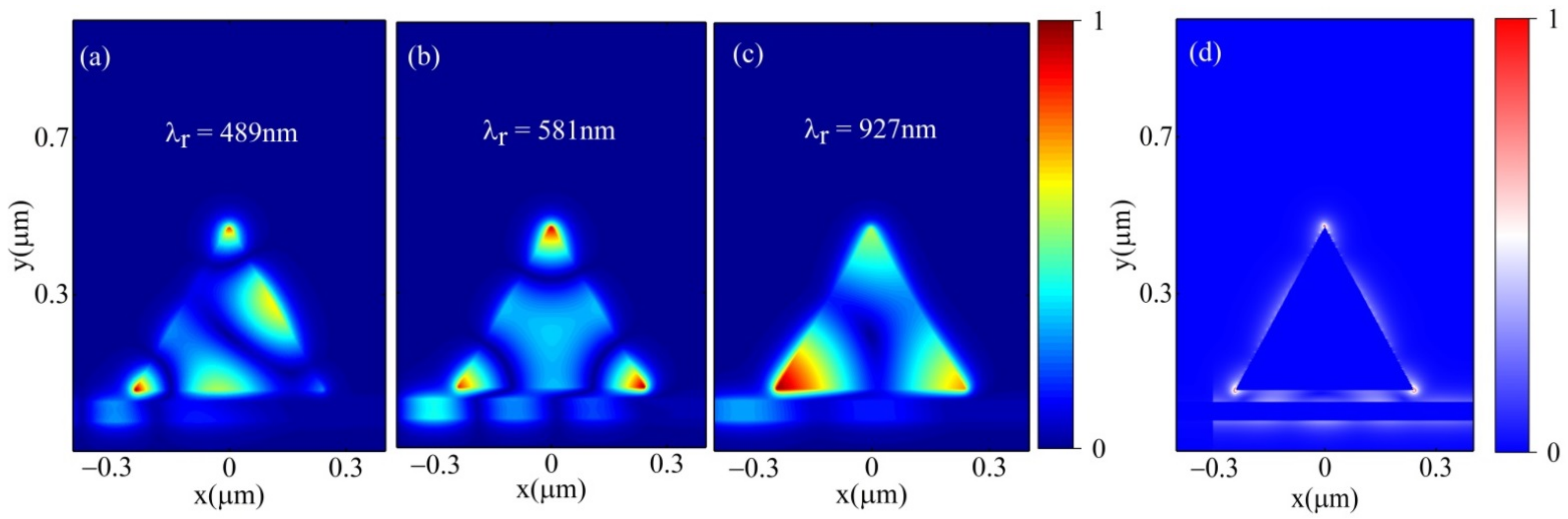
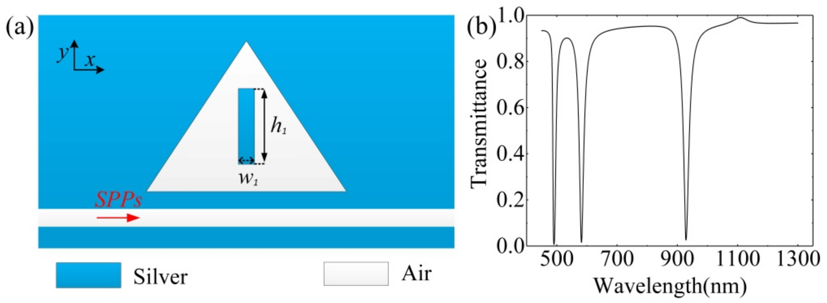
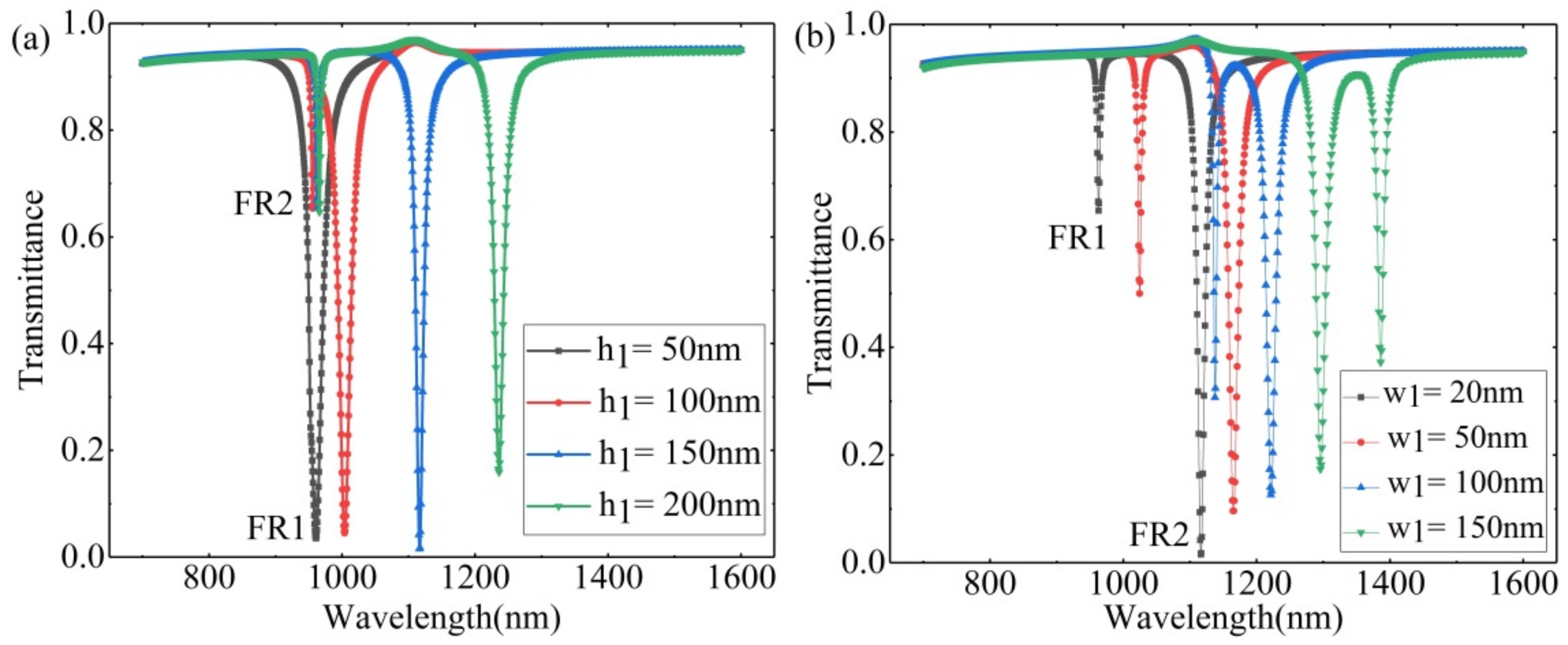
3.1. Bar Embedded ETSC Configuration

Figure 5a shows the ETSC with a bar. The height h 1 and width w 1 of bar are 100 nm and 20 nm by default. Additionally, Figure 5b indicates the transmittance spectrum of the ETSC with a bar. From Figure 5b, adding a bar into the ETSC is almost the same as the ETSC without a bar.
The transmission spectra of the structure with various heights are shown in Figure 6a. From Figure 6a, by increasing height of the bar, FR1 shifts obviously to a higher wavelength without a significant reduction in T m i n , while a new resonance mode called FR2 emerges when h 1 range from 50 nm to 100 nm, and after that, FR2 does not change with the growth of h 1 .
From Figure 6b, based on the ETSC, the effects of w 1 which increases from 20 nm to 150 nm on transmittance spectra are studied. There is an apparent tendency in Figure 6b that both FR1 and FR2 have evident redshifts, and two resonance wavelengths became closer since the increase in width, when w 1 = 100 nm the distance is at the minimum.

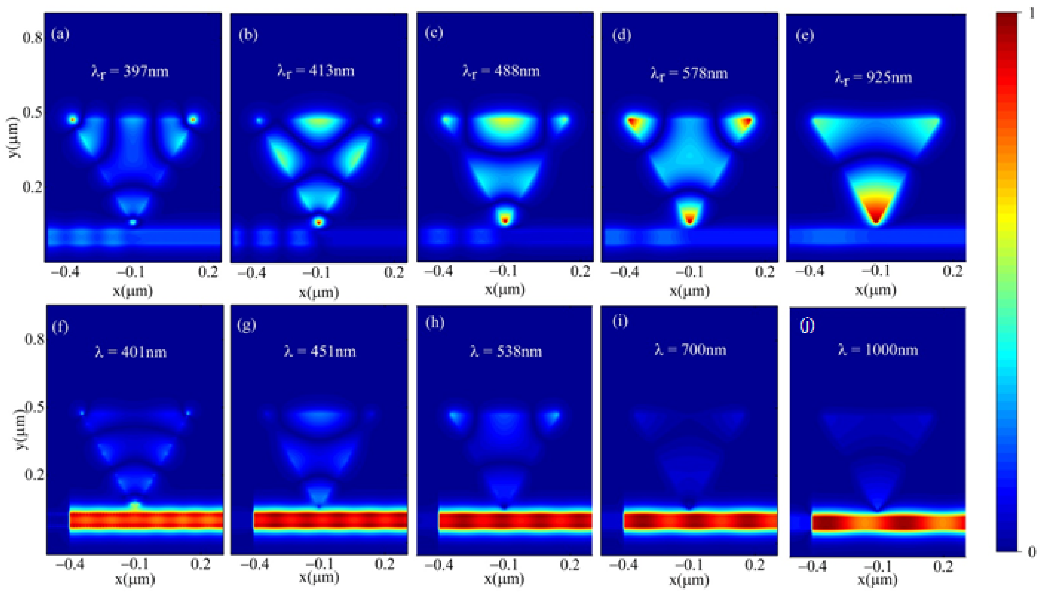
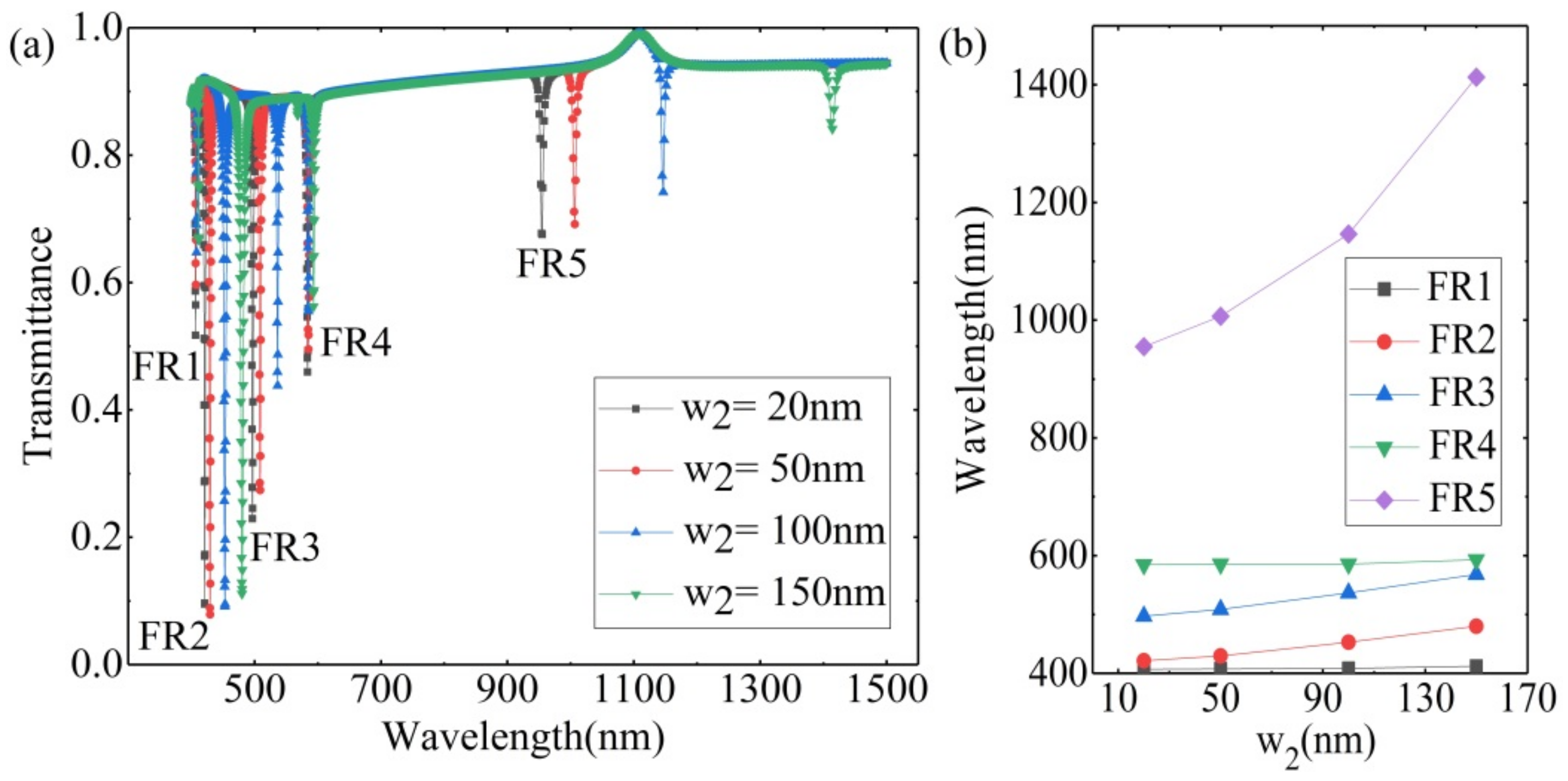
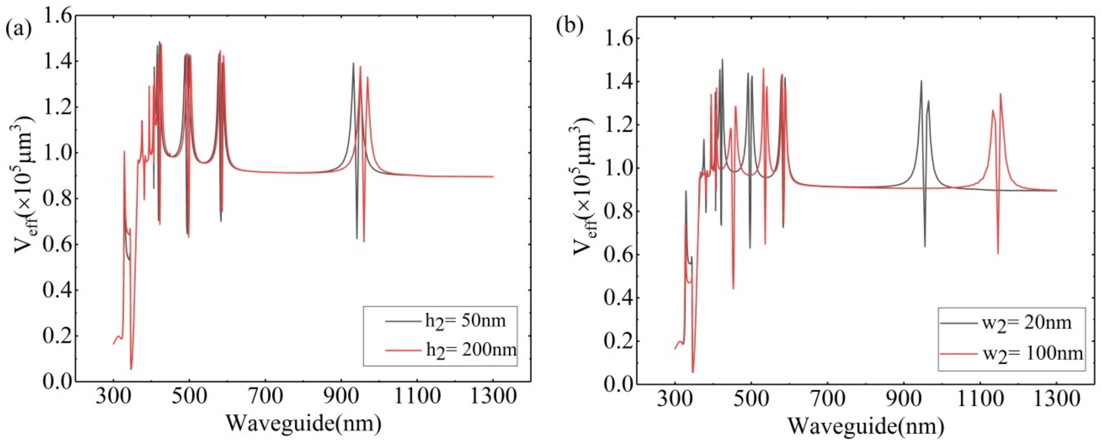
3.2. Bar Embedded the Inverted ETSC Configuration

Figure 7a denotes that the derived structure consists of the inverted ETSC and a bar, which is introduced into the inverted ETSC to realize the increase in λ r . The bar is described by two structural parameters h 2 and w 2 . h 2 and w 2 of the bar are defined as 150 nm and 20 nm by default. the structural parameters are altered independently, and the influences on the transmittance spectra are investigated. As for Figure 7b, it exhibits the transmittance spectrum of the inverted ETSC with a bar, which has little difference with the inverted ETSC only.
On the foundation of the inverted ETSC, the effects of h 2 , which climbs from 0 nm to 200 nm on the transmittance spectra, are studied, and the outcomes are depicted in Figure 8a. It is distinct that, without a significant reduction in T m i n , the resonance wavelengths of the FR1, FR2, FR3 and FR4 are almost fixed, while the FR5 has a redshift by altering h 2 . To further certify the linear performance, the resonance wavelengths of FR1, FR2, FR3, FR4 and FR5 are researched, and the results do manifest this linear relation, as is shown in Figure 8b.
After that, the transmission spectra of the structure with different widths are shown in Figure 9a. By increasing the width of the bar from 20 nm to 150 nm and keeping the other parameter constant, FR1 and FR4 are nearly fixed at their original location, while λ r of FR2 and FR3 shift to higher wavelengths. For FR5, the movement to a higher wavelength is significant. In the same way, the resonance wavelengths of FR1, FR2, FR3, FR4 and FR5 are depicted in Figure 9b. Through the range of different parameters, transmittance spectra can be better controlled to meet various demands in practice.
The sensitivity of the proposed structure in Figure 7a depends on the response degree to the change of the refractive index (RI) inside the white area of the inverted ETSC. With all the structural parameters in Figure 7a unchanged, the n increases from 1.00 to 1.16 at the step of 0.04. The performance of the proposed structure in a nanometer scale is described in Figure 10a, which indicates that these quadruple Fano resonances owe redshifts. Since the sensitivity (S) of narrowband filter can be explained as the wavelength shift per unit refractive index change, expressed as S = d λ d n (nm/RIU), the sensitivities are 923 nm/RIU, 542 nm/RIU, 427 nm/RIU, 301 nm/RIU and 250 nm/RIU at FR5, FR4, FR3, FR2 and FR1 separately, which are concluded in Figure 10b.
Moreover, FOM can be represented as F O M = S F W H M , where FWHM is the full width at half-maximum of the transmittance spectrum. From Figure 7b, different resonance wavelengths’ FOMs are calculated, in which the maximum can reach 710 at 933 nm.
Another essential factor of a filter measuring the ability to give wavelength selectivity is represented as a quality factor (Q). The quality factor can be expressed as Q = λ r F W H M . Additionally, the dephasing time of the inverted ETSC is a critical parameter that can be defined by taking into account the resonance narrowness as follows: t d = 2 δ [33]. Here, is the reduced Planck’s constant and δ = w r m a x w r m i n . w r m a x and w r m i n are corresponding to λ r m a x and λ r m i n . Therefore, the dephasing times are 5.4 × 10⁻³ fs, 5.7 × 10⁻³ fs, 1.2 × 10⁻² fs, 9.7 × 10⁻³ fs, and 2.5 × 10⁻² fs.
Another important factor is Veff which represents the effective mode volume of the confined electromagnetic field in the cavity. Additionally, the effective mode volume is calculated according to V e f f = V ε ( r ) E ( r ) 2 d V m a x ε ( r ) E ( r ) 2 [34,35,36,37,38,39,40,41,42,43,44,45,46], where ε(r) is the dielectric constant, |E(r)| is the electric field strength and V is the volume encompassing the resonator with a boundary in the radiation zone of the cavity mode. As for Figure 11a, the minimum of Veff is 0.02 × 105 μm when h 2 = 50 nm. By increasing the height of the silver bar, Veff has a slight redshift in the near-infrared band. In Figure 11b, the minimum of Veff is 0.06 × 105 μm when w 2 = 20 nm. Increasing the width of the silver bar, Veff has an obvious redshift in the near-infrared band.
To manifest the advantages of the designed structure performed as a narrowband filter, Table 1 is formed, which compares the performance characteristics of our structure with other likely designs which can produce multiple Fano resonances based on SPPs published in recent years. From Table 1, we could conclude that our structure has relatively good sensitivity and it is superior to other designs in the maximal Q.

4. Conclusions

Several plasmonic bandstop filters based on the ETSC are designed in this work. Additionally, triple and quintuple resonance modes occur when light passes through the proposed structure, including the ETSC and the inverted ETSC. By introducing a bar into the ETSC and the inverted one, structural resonant wavelengths can be increased by changing the height and width of the bar. Moreover, inverting the ETSC could reduce the FWHM of every resonance wavelength to increase Q efficiently. The main advantage of the proposed structures compared with previous methods is the better quality factor, narrow bandwidth, good sensitivity and tunability. It is believed that the proposed structures will be used in high integration plasmonic devices in future.

Author Contributions

Conceptualization, J.Z. and H.F.; data curation, J.Z.; formal analysis, J.Z.; investigation, J.Z.; methodology, J.Z.; project administration, Y.G.; resources, J.Z.; software, J.Z.; supervision, Y.G.; validation, J.Z., H.F. and Y.G.; writing—original draft, J.Z.; writing—review and editing, Y.G. All authors have read and agreed to the published version of the manuscript.

Funding

This research was funded in part by University Nursing Program for Young Scholars with Creative Talents in Heilongjiang Province (Grant No. UNPYSCT-2015016), Natural Science Foundation of Heilongjiang Province (Grant No. LH2019F047) and Project of the central government supporting the reform and development of local colleges and universities (Grant No. 2020YQ01).

Data Availability Statement

The available data have already been stated in the article.

Acknowledgments

Structure numerical simulation was provided by Lumerical Solutions, Inc.

Conflicts of Interest

The authors declare no conflict of interest.

References

  1. Chen, J.; Sun, C.; Gong, Q. Fano resonances in a single defect nanocavity coupled with a plasmonic waveguide. Opt. Lett. 2014, 39, 52–55. [Google Scholar] [CrossRef]
  2. Chou Chao, C.T.; Chou Chau, Y.F.; Huang, H.J.; Kumara, N.; Kooh, M.R.R.; Lim, C.M.; Chiang, H.P. Highly Sensitive and Tunable Plasmonic Sensor Based on a Nanoring Resonator with Silver Nanorods. Nanomaterials 2020, 10, 1399. [Google Scholar] [CrossRef]
  3. Farahani, M.; Granpayeh, N.; Rezvani, M. Improved plasmonic splitters and demultiplexers. Photonics Nanostruct. Fundam. Appl. 2013, 11, 157–165. [Google Scholar] [CrossRef]
  4. Lu, H.; Wang, G.; Liu, X. Manipulation of light in MIM plasmonic waveguide systems. Chin. Sci. Bull. 2013, 58, 3607–3616. [Google Scholar] [CrossRef] [Green Version]
  5. Li, Z.; Wen, K.; Chen, L.; Lei, L.; Zhou, J.; Zhou, D.; Fang, Y.; Wu, B. Control of Multiple Fano Resonances Based on a Subwavelength MIM Coupled Cavities System. IEEE Access 2019, 7, 59369–59375. [Google Scholar] [CrossRef]
  6. Wen, K.; Yan, L.; Pan, W.; Luo, B.; Guo, Z.; Guo, Y.; Luo, X. Electromagnetically Induced Transparency-Like Transmission in a Compact Side-Coupled T-Shaped Resonator. J. Lightwave Technol. 2014, 32, 1701–1707. [Google Scholar] [CrossRef]
  7. Kravets, V.G.; Kabashin, A.V.; Barnes, W.L.; Grigorenko, A.N. Plasmonic Surface Lattice Resonances: A Review of Properties and Applications. Chem. Rev. 2018, 118, 5912–5951. [Google Scholar] [CrossRef]
  8. Mejia-Salazar, J.R.; Oliveira, O.N., Jr. Plasmonic Biosensing. Chem. Rev. 2018, 118, 10617–10625. [Google Scholar] [CrossRef]
  9. Ahmadivand, A.; Gerislioglu, B.; Ahuja, R.; Kumar Mishra, Y. Terahertz plasmonics: The rise of toroidal metadevices towards immunobiosensings. Mater. Today 2020, 32, 108–130. [Google Scholar] [CrossRef]
  10. Gutha, R.R.; Sadeghi, S.M.; Sharp, C.; Wing, W.J. Biological sensing using hybridization phase of plasmonic resonances with photonic lattice modes in arrays of gold nanoantennas. Nanotechnology 2017, 28, 355504. [Google Scholar] [CrossRef]
  11. Sadeghi, S.M.; Wing, W.J.; Campbell, Q. Tunable plasmonic-lattice mode sensors with ultrahigh sensitivities and figure-of-merits. J. Appl. Phys. 2016, 119, 244503. [Google Scholar] [CrossRef]
  12. Huang, L.; Ding, L.; Zhou, J.; Chen, S.; Chen, F.; Zhao, C.; Xu, J.; Hu, W.; Ji, J.; Xu, H.; et al. One-step rapid quantification of SARS-CoV-2 virus particles via low-cost nanoplasmonic sensors in generic microplate reader and point-of-care device. Biosens. Bioelectron. 2021, 171, 112685. [Google Scholar] [CrossRef]
  13. Fano, U. Effects of Configuration Interaction on Intensities and Phase Shifts. Phys. Rev. 1961, 124, 1866–1878. [Google Scholar] [CrossRef]
  14. Anderson, P.W. Localized Magnetic States in Metals. Phys. Rev. 1961, 124, 41–53. [Google Scholar] [CrossRef]
  15. Akhavan, A.; Ghafoorifard, H.; Abdolhosseini, S.; Habibiyan, H. Metal–insulator–metal waveguide-coupled asymmetric resonators for sensing and slow light applications. IET Optoelectron. 2018, 12, 220–227. [Google Scholar] [CrossRef]
  16. Chou Chau, Y.-F. Mid-infrared sensing properties of a plasmonic metal–insulator–metal waveguide with a single stub including defects. J. Phys. D Appl. Phys. 2020, 53, 115401. [Google Scholar] [CrossRef]
  17. Butt, M.A.; Kazanskiy, N.L.; Khonina, S.N. Nanodots decorated asymmetric metal–insulator–metal waveguide resonator structure based on Fano resonances for refractive index sensing application. Laser Phys. 2020, 30, 076204. [Google Scholar] [CrossRef]
  18. Fang, Y.; Sun, M. Nanoplasmonic waveguides: Towards applications in integrated nanophotonic circuits. Light Sci. Appl. 2015, 4, e294. [Google Scholar] [CrossRef] [Green Version]
  19. Wang, S.; Yu, S.; Zhao, T.; Wang, Y.; Shi, X. A nanosensor with ultra-high FOM based on tunable malleable multiple Fano resonances in a waveguide coupled isosceles triangular resonator. Opt. Commun. 2020, 465, 125614. [Google Scholar] [CrossRef]
  20. Zhang, Z.; Wang, J.; Zhao, Y.; Lu, D.; Xiong, Z. Numerical Investigation of a Branch-Shaped Filter Based on Metal-Insulator-Metal Waveguide. Plasmonics 2011, 6, 773–778. [Google Scholar] [CrossRef]
  21. Zhang, Z.; Yang, J.; He, X.; Han, Y.; Zhang, J.; Huang, J.; Chen, D. Plasmonic Filter and Demultiplexer Based on Square Ring Resonator. Appl. Sci. 2018, 8, 462. [Google Scholar] [CrossRef] [Green Version]
  22. Gramotnev, D.K.; Bozhevolnyi, S.I. Plasmonics beyond the diffraction limit. Nat. Photonics 2010, 4, 83–91. [Google Scholar] [CrossRef]
  23. Butt, M.A.; Kazanskiy, N.L.; Khonina, S.N. Highly Sensitive Refractive Index Sensor Based on Plasmonic Bow Tie Configuration. Photonic Sens. 2020, 10, 223–232. [Google Scholar] [CrossRef]
  24. Yu, S.; Wang, S.; Zhao, T.; Yu, J. Tunable Plasmonic System Based on a Slotted Side-Coupled Disk Resonator and Its Multiple Applications on Chip-Scale Devices. Optik 2020, 212, 164748. [Google Scholar] [CrossRef]
  25. Yan, S.; Shi, H.; Yang, X.; Guo, J.; Wu, W.; Hua, E. Study on the Nanosensor Based on a MIM Waveguide with a Stub Coupled with a Horizontal B-Type Cavity. Photonics 2021, 8, 125. [Google Scholar] [CrossRef]
  26. Yang, X.; Hu, X.; Yang, H.; Gong, Q. Ultracompact all-optical logic gates based on nonlinear plasmonic nanocavities. Nanophotonics 2017, 6, 365–376. [Google Scholar] [CrossRef]
  27. Wang, Y.; Xue, B.; Mao, J.; Lu, M. Plasmonic-induced transparency in a metallic stub with two cuts and transmission line model. J. Mod. Opt. 2018, 65, 2301–2307. [Google Scholar] [CrossRef]
  28. Le-Van, Q.; Zoethout, E.; Geluk, E.J.; Ramezani, M.; Berghuis, M.; Rivas, J.G. Enhanced Quality Factors of Surface Lattice Resonances in Plasmonic Arrays of Nanoparticles. Adv. Opt. Mater. 2019, 7, 8. [Google Scholar] [CrossRef]
  29. Bin-Alam, M.S.; Reshef, O.; Mamchur, Y.; Alam, M.Z.; Carlow, G.; Upham, J.; Sullivan, B.T.; Menard, J.M.; Huttunen, M.J.; Boyd, R.W.; et al. Ultra-high-Q resonances in plasmonic metasurfaces. Nat. Commun. 2021, 12, 974. [Google Scholar] [CrossRef]
  30. Jeong, P.A.; Goldflam, M.D.; Campione, S.; Briscoe, J.L.; Vabishchevich, P.P.; Nogan, J.; Sinclair, M.B.; Luk, T.S.; Brener, I. High Quality Factor Toroidal Resonances in Dielectric Metasurfaces. ACS Photonics 2020, 7, 1699–1707. [Google Scholar] [CrossRef]
  31. Ma, L.; Zheng, W.X.; Li, J.; Chen, D.X.; Wang, W.J.; Liu, Y.F.; Zhou, Y.D.; Yang, Y.J.; Huang, Y.J.; Wen, G.J. High-Q Hg-anapole resonator with microstrip line coupling for high-precision temperature sensing applications. Results Phys. 2021, 24, 5. [Google Scholar] [CrossRef]
  32. Dong, L.; Xu, X.; Sun, K.; Ding, Y.; Ouyang, P.; Wang, P. Sensing analysis based on fano resonance in arch bridge structure. J. Phys. Commun. 2018, 2, 105010. [Google Scholar] [CrossRef] [Green Version]
  33. Gupta, M.; Singh, R. Terahertz Sensing with Optimized Q /Veff Metasurface Cavities. Adv. Opt. Mater. 2020, 8, 1902025. [Google Scholar] [CrossRef]
  34. Ahmadivand, A.; Gerislioglu, B.; Ramezani, Z. Gated graphene island-enabled tunable charge transfer plasmon terahertz metamodulator. Nanoscale 2019, 11, 8091–8095. [Google Scholar] [CrossRef]
  35. Min, B.; Ostby, E.; Sorger, V.; Ulin-Avila, E.; Yang, L.; Zhang, X.; Vahala, K. High-Q surface-plasmon-polariton whispering-gallery microcavity. Nature 2009, 457, 455–458. [Google Scholar] [CrossRef] [PubMed]
  36. Gierak, J.; Madouri, A.; Biance, A.L.; Bourhis, E.; Patriarche, G.; Ulysse, C.; Lucot, D.; Lafosse, X.; Auvray, L.; Bruchhaus, L.; et al. Sub-5nm FIB direct patterning of nanodevices. Microelectron. Eng. 2007, 84, 779–783. [Google Scholar] [CrossRef]
  37. Li, G.; Winick, K.A.; Griffin, H.C.; Joseph, S. Hayden Systematic modeling study of channel waveguide fabrication by thermal silver ion exchange. Appl. Opt. 2006, 45, 743–755. [Google Scholar] [CrossRef]
  38. Stewart, G.; Millar, C.A.; Laybourn, P.J.R.; Wilkinson, C.D.W.; Delarue, R.M. Planar Optical Waveguides Formed by Silver-Ion Migration in Glass. IEEE J. Quantum Electron. 1977, 13, 192–200. [Google Scholar] [CrossRef]
  39. Asgari, S.; Pooretemad, S.; Granpayeh, N. Plasmonic refractive index sensor based on a double concentric square ring resonator and stubs. Photonics Nanostruct. Fundam. Appl. 2020, 42, 100857. [Google Scholar] [CrossRef]
  40. Moradiani, F.; Farmani, A.; Mozaffari, M.H.; Seifouri, M.; Abedi, K. Systematic engineering of a nanostructure plasmonic sensing platform for ultrasensitive biomaterial detection. Opt. Commun. 2020, 474, 126178. [Google Scholar] [CrossRef]
  41. Rakhshani, M.R. Optical refractive index sensor with two plasmonic double-square resonators for simultaneous sensing of human blood groups. Photonics Nanostruct. Fundam. Appl. 2020, 39, 100768. [Google Scholar] [CrossRef]
  42. Rakhshani, M.R. Wide-angle perfect absorber using a 3D nanorod metasurface as a plasmonic sensor for detecting cancerous cells and its tuning with a graphene layer. Photonics Nanostruct. Fundam. Appl. 2021, 43, 100883. [Google Scholar] [CrossRef]
  43. Rakhshani, M.R.; Mansouri-Birjandi, M.A. A high-sensitivity sensor based on three-dimensional metal–insulator–metal racetrack resonator and application for hemoglobin detection. Photonics Nanostruct. Fundam. Appl. 2018, 32, 28–34. [Google Scholar] [CrossRef]
  44. To, N.; Juodkazis, S.; Nishijima, Y. Detailed Experiment-Theory Comparison of Mid-Infrared Metasurface Perfect Absorbers. Micromachines 2020, 11, 409. [Google Scholar] [CrossRef] [PubMed] [Green Version]
  45. Nishijima, Y.; Balčytis, A.; Naganuma, S.; Seniutinas, G.; Juodkazis, S. Kirchhoff’s metasurfaces towards efficient photo-thermal energy conversion. Sci. Rep. 2019, 9, 8284. [Google Scholar] [CrossRef]
  46. Nishijima, Y.; Balčytis, A.; Naganuma, S.; Seniutinas, G.; Juodkazis, S. Tailoring metal and insulator contributions in plasmonic perfect absorber metasurfaces. ACS Appl. Nano Mater. 2018, 1, 3557–3564. [Google Scholar] [CrossRef]
Figure 1. (a) The schematic of the equilateral triangle-shaped cavity (ETSC); (b) the transmission spectra of the ETSC by using coupled mode theory (CMT) and Johnson and Christy model.
Photonics 08 00244 g001
Figure 2. The magnetic distribution profile of the ETSC at: (a) λ r = 489 nm; (b) λ r = 581 nm; (c) λ r = 927 nm; (d) the vectorial charge distribution of the ETSC at λ r = 489 nm.
Photonics 08 00244 g002
Figure 3. (a) The schematic of the inverted ETSC; (b) the transmittance spectrum of the inverted ETSC.
Photonics 08 00244 g003
Figure 4. The magnetic distribution profile of the inverted ETSC at: (a) λ r = 397 nm; (b) λ r = 413 nm; (c) λ r = 488 nm; (d) λ r = 578 nm; (e) λ r = 925 nm; (f) λ = 401 nm; (g) λ = 451 nm; (h) λ = 538 nm; (i) λ = 700 nm; (j) λ = 1000 nm.
Photonics 08 00244 g004
Figure 5. (a) The schematic of the ETSC with a bar; (b) the transmittance spectrum of the ETSC with a bar.
Photonics 08 00244 g005
Figure 6. (a) The transmission spectra of different h 1 ; (b) the transmission spectra of different w 1 .
Photonics 08 00244 g006
Figure 7. (a) The schematic of the inverted ETSC added with a bar; (b) the transmittance spectrum of the inverted ETSC with a bar.
Photonics 08 00244 g007
Figure 8. (a) The transmittance spectra for different h 2 ; (b) the resonance wavelength of FR1, FR2, FR3, FR4 and FR5 with different h 2 .
Photonics 08 00244 g008
Figure 9. (a) The transmittance spectra of different w 2 ; (b) the resonance wavelength of FR1, FR2, FR3, FR4 and FR5 with different w 2 .
Photonics 08 00244 g009
Figure 10. (a) The transmittance spectra of the designed structure with n varying from 1 to 1.16; (b) the resonance wavelength of FR1, FR2, FR3, FR4 and FR5 with different n.
Photonics 08 00244 g010
Figure 11. (a) Effective mode volume (Veff) for different heights of the inverted ETSC; (b) Veff for different widths of the inverted ETSC.
Photonics 08 00244 g011
Table 1. Comparison of the proposed structure with the latest relative designs.
ReferencesTypeQSFOMtdVeff
[4]Single29.67208029.92NN
[15]DualMax 31.1Max 2300Max 31.5NN
[16]Dual106/123900/1700Max 1.38 × 105NN
This workQuintupleMax 322923/542/427/301/250Max 710Min 5.4 × 10⁻³ fsMin 0.02 × 105 μm
Q: represents quality factor. S: represents sensitivity. FOM: represents figure of merit. td: represents dephasing time.
Publisher’s Note: MDPI stays neutral with regard to jurisdictional claims in published maps and institutional affiliations.

