Article

Plasmonic Enhanced InP Nanowire Array Solar Cell through Optoelectronic Modeling

1
Faculty of Electrical Engineering, Shahid Rajaee Teacher Training University, Tehran 16788-15811, Iran
2
Nano-Photonics and Optoelectronics Research Laboratory (NORLab), Shahid Rajaee Teacher Training University, Tehran 16788-15811, Iran
*
Author to whom correspondence should be addressed.
Photonics 2021, 8(4), 90; https://doi.org/10.3390/photonics8040090
Submission received: 1 March 2021 / Revised: 22 March 2021 / Accepted: 23 March 2021 / Published: 25 March 2021

Abstract

:
Vertical nanowire (NW) arrays are a promising candidate for the next generation of the optoelectronics industry because of their significant features. Here, we investigated the InP NW array solar cells and obtained the optoelectronic properties of the structure. To improve the performance of the NW array solar cells, we placed a metal layer of Au at the bottom of the NWs and considered their top part to be a conical-shaped parabola. Using optical and electrical simulations, it has been shown that the proposed structure improves the absorption of light in normal incidence, especially at wavelengths near the bandgap of InP, where photons are usually not absorbed. Under inclined radiation, light absorption is also improved in the middle part of the solar spectrum. Increased light absorption in the cell led to the generation of more electron–hole pairs, resulting in an increase in short circuit current density from 24.1 mA/cm2 to 27.64 mA/cm2, which is equivalent to 14.69% improvement.

1. Introduction

Photovoltaics, first introduced in 1958, is a process in which light is converted directly into electricity. Various materials and techniques are used to make solar cells based on the cost and efficiency of conversion. The first material used was silicon, which had disadvantages such as low efficiency. The second generation of solar cells was thin-film solar cells for producing electrical power, which received a lot of attention due to the use of thin layers in their structure [1]. Then, following further research in the field of photovoltaics technology to achieve new structures, the vertical arrays of III-V direct band gap semiconductor nanowire (NWs) were considered due to the reduction in the volume of material consumed compared to planar structures.
The low cost and other features of semiconductor NW structures have led to great interest in their use in a variety of applications, including photodetectors [1,2,3], light-emitting diodes [4,5,6], and lasers [7,8]. In NW array solar cells, proper design and improved absorption of excited optical modes are effective factors in optimizing photovoltaic efficiency. One of the common strategies to achieve these points is the proper design of the structure geometry. For example, increasing the length of the NW, which reduces the light transmission at the NW/substrate interface, increases the volume of consumables, and decreases the efficiency due to the increase in the dark current of the solar cell. Furthermore, the reduction of the pitch leads to a stronger absorption but increases the top insertion reflection losses. Another strategy to improve the absorption characteristic of NWs is to break the symmetry of the incident light/NW system. Oblique radiation stimulates new polarization-dependent optical modes. However, the improvement is limited to a narrow band of the solar spectrum. One way to increase light absorption in NWs is to reduce light transmission at the NW-substrate interface and reduce light reflection at the NW/superstrate interface. Another way to improve the absorption in solar cell structures is to use the plasmonic effect. In this effect with light irradiation, charge carriers at the metal and the dielectric boundary with positive or negative permittivity begin collective oscillation and produce surface plasmon resonance (SPR).
Surface plasmon resonances are divided into two categories, localized surface plasmon resonance (LSPR) and surface plasmon polariton (SPP). LSPRs are observed when surface plasmon is confined in the subwavelength nanostructure, and SPPs are caused by the propagation of charge carriers along the planar surface. Upon excitation, both forms of SPRs can confine incident light on a low-subwavelength scale. The confinement of some carriers improves the local field and allows the manipulation of light below the diffraction limit. These remarkable SPR features allow plasmonic materials to be used in a variety of fields, including photonics [9], energy [10,11,12], sensors [13], and more. For example, metal nanoparticles inside thin-film solar cells act as antennas that capture the incident light and store its energy in LSPR modes [14,15,16]. This energy can be transferred to the semiconductor layer by near-field coupling or scattered to the active layer by metal nanoparticles. Nanoparticles can also be used as front scatterers or back reflectors [17,18,19,20,21].
The metal nanostructures at the front trap light in the solar cell beneath by forward scattering the incident light at their LSPR wavelengths with a scattering cross-section greater than their geometric cross-section. Plasmonic nanoparticles at the back of the solar cell increase the optical thickness and improve performance by scattering the far-field. In this theoretical study, we present a structure in which a layer of Au metal was placed at the bottom of the NW to prevent the transmission of light into the substrate and reflect the light that is not absorbed in the single pass into the NW. Increasing the optical path length of excited modes led to improved absorption and photovoltaic efficiency without increasing the volume of material used. More recently, with the development of nanotechnology, the use of metamaterials in many applications such as biosensors [22], photodetectors [23], and absorbers [24,25] was considered. This method can be beneficial in solar harvesting as well.
Furthermore, by considering the conical-shaped parabola on the top of the NW, we reduced leakage of the light into the space outside the NW from the top. The proposed structure is a new method to improve the performance of the NW array solar cell and achieve absorption of over 90% at wavelengths close to the band gap wavelength of InP.

2. Materials and Methods

In this work, we investigated a square array of vertical InP NWs with Au layer at the bottom and conical-shaped parabola at the top. Cone-shaped nanowires grown in vapor-liquid-solid (VLS) mode are a good candidate for the fabrication of low-cost high-performance solar cells. Thus, this shape of nanowires can be beneficial in solar cells. Methods of fabrication of this kind of nanowire are presented in [26]. According to [27], we can place an Au layer at the bottom of the nanowire. Figure 1 shows a schematic of the proposed structure (with Au layer at the bottom and conical-shaped parabola at the top of NWs).
Here, we calculate the absorption of incident photons and the separation of electron–hole pairs photogenerated over an axial n-i-p junction for the InP NW array. The optical response of the NW array is calculated by solving the Maxwell’s equations using tabulated data for the refractive indices of InP [28]. Electron–hole transfer in NWs is solved using the drift–diffusion formulas. We use the finite element method (FEM) for this numerical analysis.
The solutions of Maxwell’s equations show how light is distributed inside and outside of the NWs. By obtaining the electric field of the system, E(r), the number of electron–hole pairs photogenerated per unit volume per unit time, G(r), can be obtained for a given incident intensity spectrum. The absorption at each wavelength on the volume V of the NW can be calculated by:
A λ = 1 2 ω ε 0 E λ 2 Im n 2 λ dV
where ε 0 is the vacuum permittivity, ω is the angular frequency, E is the electric field, and n is the complex refractive index.
After calculating the optical generation rate, G(r), and recombination mechanisms, R, the electron–hole transfer is analyzed by solving the drift–diffusion equations presented below:
. ε φ = q p n + N D N A , . J n = . q μ n n φ n = q R G , . J p = . q μ p p φ p = q R G ,
R is the net recombination rate in the bulk of the NW obtained from:
R = R SRH   + R Rad   + R Aug = A n + p + 2 n i + B + C n + p np n i 2 ,
where A, B, and C are the recombination coefficient of the SRH/Radiative/Auger recombination, and ni is the intrinsic carrier concentration. We neglect radiative recombination and we use B = 0 in Equation (3). We assume that the Shockley–Read–Hall (SRH) lifetime and the Auger recombination coefficient for both electron and holes are equal. The surface recombination at the surface of the NW is also considered through the term:
R surface = ν s r n + p + 2 n i n p + n i 2 ,
where ν s r is the surface recombination velocity [29].
Assuming that all the photogenerated carriers contribute to the current, we can obtain the short circuit current density from:
J s c = e λ hc P abs λ P in λ I AM 1.5 λ d λ ,
The geometric structure used for the drift–diffusion model has a length of 100 nm in top n-segment and 300 nm in bottom p-segment with 1018 cm−3 ionized doping concentration for both of them. The i-segment with 1015 cm−3 p-doping concentration is located between the n- and p-segments.
The calculations are performed using the finite-difference time-domain (FDTD) method at a wavelength range of 320–1000 nm for unpolarized incident light parallel to the axis of the NWs, taking into account the periodic boundary conditions in the x-, y- directions and perfectly matched layer (PML) in the z-direction. The specific values of the parameters used in the drift–diffusion model are presented in Table 1. We consider here, surface recombination velocity for the bare cell without Au layer at the bottom and conical-shaped parabola at the top equals to 20,000 cms−1 [30]. Placing the Au layer at the bottom of the NWs causes a change in the motion of the electrons, which is considered in modeling by changing the surface recombination velocity. The value of this surface recombination velocity is selected according to reference [31]. Reflection is monitored with a power monitor placed behind the radiation source; transmission is monitored with a power monitor placed behind the structure. Electric and magnetic fields are detected within the frequency profile monitors. For a solar cell, in addition to the efficiency of converting sunlight into electrical energy, η, three other parameters are usually considered: (1) the short circuit current density Jsc, (2) the open circuit voltage Voc, and (3) the fill factor FF defined by η = J sc V oc   FF P in .

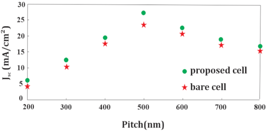
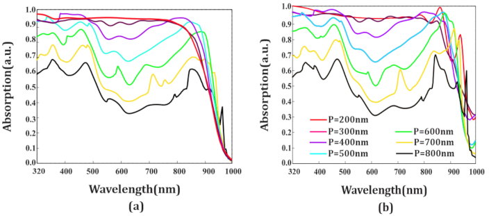
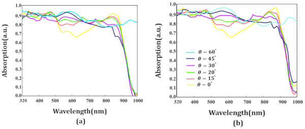
3. Results and Discussion

As mentioned in previous works [34,35,36,37], light absorption in NWs depends on the geometrical parameters, and with proper design, light absorption can be improved in them. One way to improve the absorption of light to achieve almost complete absorption in NWs is to increase their length. Increasing this parameter reduces the transmission of light to the substrate, but in solar cells it increases the dark current, which results in decreased structural efficiency. Furthermore, with increasing length, the volume of materials used increases. Increasing the radius of the NWs increases the absorption of light in them, but due to the increase in light transmission between the NWs and the substrate, the current of the structure decreases. In addition, by reducing the pitch of the array, the absorption of coupled light into the array increases. However, the problem is the increase in top-insertion reflection losses.
In this study, to reduce the transfer of guided modes into the substrate without changing the geometrical parameter of the NWs, we placed a layer of Au metal at the bottom of the NWs which are placed in a square lattice with geometrical values of radius of 100 nm, pitch of 500 nm, and length of 1400 nm. The geometrical values of the radius and the pitch are chosen so that the NWs form a sparse array and the results are independent of the lattice arrangement [38]. Furthermore, the length of 1400 nm for the total length (with or without Au layer) is chosen so that the absorption saturation that is seen in long NWs does not occur [30,39,40].
Because most of the light in the NWs is absorbed in the top parts and the absorption decreases as it moves towards the bottom, we placed Au layer at the bottom to act as a reflector at optical frequencies and reflect light into the NWs. This reflection increases the optical path length of the excited modes and improves the absorption of the guided modes. In addition, when the light reaches to the metal, plasmon is excited in metal and it generates dipole. Due to dipole–dipole coupling between the plasmon excited metal and the adjacent semiconductor in near-field, plasmonic energy in the metal is transferred to semiconductor and it generates more electron–hole pairs in the semiconductor. This can promote performance of the solar cell. Therefore, placing the Au layer at the bottom of the NW has a better result than other parts. By placing the Au layer on the top part of the NW, the light cannot reach the lower part of the NW and the light absorption is reduced.
Decreased light absorption also reduces the number of photogenerated carriers compared to the bare structure. To determine the appropriate thickness of the Au layer, one must sweep its thickness from 0 to 250 nm, and obtain the Jsc each time. According to the results presented in Figure 2, sweeping the thickness of this layer has little effect on the Jsc. Among the various values, 80 nm thickness gives the maximum improvement in Jsc. In this case, the Jsc increases from 24.1 mA/cm2 for the bare cell to 26.75 mA/cm2, which is equivalent to a 10% improvement.
In NWs with the same geometry, we can improve the absorption if we can reduce the reflection of light from the NW/superstrate. To achieve this goal, we consider the top part of the NW, which is the interface between air and NW, in the form of a conical-shaped parabola. With this assumption, as can be seen in Figure 3, the light reflection from the top part decreases and the absorption in the NW increases. This increase in absorption increases Jsc from 24.1 mA/cm2 for the bare cell to 24.931 mA/cm2 for the NW with conical-shaped parabola on the top.
Considering that the use of an Au layer at the bottom of the NW and the conical-shaped parabola on the top part both cause more light to be trapped and more electrons and holes are generated by the light, in the following we will examine the effect of applying both of them on the performance of the array. According to the results presented in Figure 4, the absorption increases at all wavelengths, and close to the band gap wavelength of InP is approximately 1 and is limited by the reflection losses at the top side.
Observation of the electric field distribution profile within the NWs in Figure 5 for the bare cell and proposed cell shows that the Au layer prevents the transmission of light into the substrate and reflects most of the light into the NW. Thus, the modes are broadening and the absorption at the bottom of the NW is improved. By improving the absorption within the NW, more carriers contribute to the production of current and the Jsc increases from 24.1 mA/cm2 to 27.64 mA/cm2.
Since the performance of the NWs depends on the geometric parameters of the structure, we sweep the radius and pitch parameters and examine their effects. As shown in Figure 6, sweeping the radius up to about 50 nm does not cause a significant change in the Jsc of the proposed cell relative to the bare cell. As can be seen in Figure 7, as the radius increases, the absorption spectrum of the proposed cell expands to longer wavelengths, and the location of the wavelength of HE11 mode, which is equivalent to the absorption peak at the longest wavelength and close to the InP band gap wavelength, red-shifts.
In Figure 8, the Jsc is plotted as a function of pitch of the array. Increasing this parameter reduces the semiconductor material in the NW, which leads to a decrease in the absorption in the NW, as can be seen in Figure 9.
According to Figure 10, by increasing pitch of the array, the insertion reflection losses at the top air/NW interface, which are an upper limit on the Jsc decrease and the absorption in the NWs can be improved. Therefore, it is necessary to choose the pitch of the array in such a way that the volume of material consumed is sufficient for absorption and the insertion reflection losses are reduced.
Another way to improve the absorption of NWs, especially in the middle part of the solar spectrum, is to break the symmetry of the NW array/light incident system, which can be achieved by obliquely incident light on the vertical NWs. In addition to the HE1m-guided modes, which depend on symmetry and are excited in the NWs, oblique radiation also stimulates additional Mie resonances. In this way we can achieve broadband absorption.
As can be seen in Figure 11, the absorption improvement occurs in a broad spectral range for inclined radiation compared to normal radiation for both bare and proposed structures. Improved absorption due to the excitation of additional modes indicates strong light trapping in the NWs and prevents its transmission to the substrate. Figure 12 shows the effect of inclined radiation on the transmission spectrum of both bare and proposed cells.
Figure 13 shows the changes in the Jsc by changing the radiation angle. Increasing the absorption of light in oblique radiation compared to normal radiation has increased the generation of the optical carriers, which leads to an increase in Jsc. Among the various radiation angles studied, the 60 ° angle achieves the greatest improvement in Jsc.
Quantitative performance of the cell can be estimated according to the current density–voltage curve obtained by solving the Poisson and drift–diffusion equations with bulk conditions and surface recombination and parameters listed in Table 1. The proposed structure which consists of a layer of Au at the bottom of the NW and a conical-shaped parabola at the top improves the Jsc by 14.69%. The power conversion efficiency varies from 14.7 for the bare cell to 17 for the proposed cell.
If we replace the ohmic contacts with carrier selective contact, the Jsc will increase from 24.1 mA/cm2 to 24.71 mA/cm2 for the bare cell and 27.64 mA/cm2 to 28.2 mA/cm2 for the proposed cell due to neglecting the recombination of minority carriers in the contacts [41]. The results of the electrical simulation for the ohmic and carrier selective contacts shown in Figure 14 are summarized in Table 2.

4. Conclusions

We theoretically investigated an InP NW array solar cell with an Au layer at the bottom and a conical-shaped parabola at the top with an axial n-i-p junction on each NW. Among the various values studied for the thickness of the Au layer, at the thickness of 80 nm, the highest improvement was obtained compared to the bare structure. According to the results, the use of Au layer at the bottom of the NWs prevented the transmission of light into the substrate and improved the absorption at long wavelengths, especially around the band gap wavelength, where light absorption was usually poor. The light trapping due to the multiple reflections of the Au layer increased the optical path length of the excited modes in the NWs. Enhancing the absorption of light also increased the photogenerated carriers and ultimately increased the Jsc. The conical-shaped parabola of the top part of the NW also reduced light reflection from the upper part of the structure and improved cell performance. The proposed structure increased Jsc from 24.1 mA/cm2 for the bare cell to 27.64 mA/cm2 for the proposed cell with ohmic contacts and from 24.71 mA/cm2 to 28.2 mA/cm2 for the carrier selective contacts, which improved to 14.69% and 14.12%, respectively.

Author Contributions

F.A. designed and performed simulations and analyzed data, S.O. edited and prepared the final draft of the manuscript. All authors have read and agreed to the published version of the manuscript.

Funding

This research received no external funding.

Data Availability Statement

Not applicable.

Acknowledgments

This work has been done in Nano-photonics and Optoelectronics Research La- boratory (NORLab), Shahid Rajaee University.

Conflicts of Interest

The authors declare that they have no known competing financial interests or personal relationships that could have appeared to influence the work reported in this paper.

References

  1. Mauthe, S.; Baumgartner, Y.; Sousa, M.; Ding, Q.; Rossell, M.D.; Schenk, A.; Czornomaz, L.; Moselund, K.E. High-speed III-V nanowire photodetector monolithically integrated on Si. Nat. Commun. 2020, 11, 1–7. [Google Scholar] [CrossRef]
  2. Shen, L.; Pun, E.Y.; Ho, J.C. Recent developments in III–V semiconducting nanowires for high-performance photodetectors. Mater. Chem. Front. 2017, 1, 630–645. [Google Scholar] [CrossRef]
  3. Ren, D.; Azizur-Rahman, K.M.; Rong, Z.; Juang, B.-C.; Somasundaram, S.; Shahili, M.; Farrell, A.C.; Williams, B.S.; Huffaker, D.L. Room-temperature midwavelength infrared InAsSb nanowire photodetector arrays with Al2O3 passivation. Nano Lett. 2019, 19, 2793–2802. [Google Scholar] [CrossRef] [PubMed]
  4. Berg, A.; Yazdi, S.; Nowzari, A.; Storm, K.; Jain, V.; Vainorius, N.; Samuelson, L.; Wagner, J.B.; Borgström, M.T. Radial Nanowire Light-Emitting Diodes in the (AlxGa1–x)yIn1–yP Material System. Nano Lett. 2016, 16, 656–662. [Google Scholar] [CrossRef] [Green Version]
  5. Gagliano, L.; Kruijsse, M.; Schefold, J.D.; Belabbes, A.; Verheijen, M.A.; Meuret, S.; Koelling, S.; Polman, A.; Bechstedt, F.; Haverkort, J.E. Efficient Green Emission from Wurtzite Al x In1–x P Nanowires. Nano Lett. 2018, 18, 3543–3549. [Google Scholar] [CrossRef] [PubMed]
  6. Bui, H.Q.T.; Velpula, R.T.; Jain, B.; Aref, O.H.; Nguyen, H.-D.; Lenka, T.R.; Nguyen, H.P.T. Full-color InGaN/AlGaN nanowire micro light-emitting diodes grown by molecular beam epitaxy: A promising candidate for next generation micro displays. Micromachines 2019, 10, 492. [Google Scholar] [CrossRef] [Green Version]
  7. Kim, H. III-V Semiconductor Nanowire Lasers on Silicon; UCLA: Los Angeles, CA, USA, 2018. [Google Scholar]
  8. Zhang, G.; Takiguchi, M.; Tateno, K.; Tawara, T.; Notomi, M.; Gotoh, H. Telecom-band lasing in single InP/InAs heterostructure nanowires at room temperature. Sci. Adv. 2019, 5, eaat8896. [Google Scholar] [CrossRef] [Green Version]
  9. Gao, Y.; Murai, S.; Zhang, F.; Tamura, S.; Tomita, K.; Tanaka, K. Enhancing upconversion photoluminescence by plasmonic-photonic hybrid mode. Opt. Express 2020, 28, 886–897. [Google Scholar] [CrossRef] [PubMed]
  10. Singh, B.; Shabat, M.M.; Schaadt, D.M. Wide angle antireflection in metal nanoparticles embedded in a dielectric matrix for plasmonic solar cells. Prog. Photovolt. Res. Appl. 2020, 28, 682–690. [Google Scholar] [CrossRef]
  11. Samajdar, D. Performance enhancement of Nanopyramid based Si hybrid solar cells utilizing the plasmonic properties of oxide coated Metal Nanoparticles. Opt. Mater. 2020, 107, 110166. [Google Scholar]
  12. Ghahremanirad, E.; Olyaee, S.; Hedayati, M. The Influence of Embedded Plasmonic Nanostructures on the Optical Absorption of Perovskite Solar Cells. Photonics 2019, 6, 37. [Google Scholar] [CrossRef] [Green Version]
  13. Liu, B.; Chen, S.; Zhang, J.; Yao, X.; Zhong, J.; Lin, H.; Huang, T.; Yang, Z.; Zhu, J.; Liu, S. A plasmonic sensor array with ultrahigh figures of merit and resonance linewidths down to 3 nm. Adv. Mater. 2018, 30, 1706031. [Google Scholar] [CrossRef]
  14. Pathak, N.K.; Chander, N.; Komarala, V.K.; Sharma, R. Plasmonic perovskite solar cells utilizing Au@SiO 2 core-shell nanoparticles. Plasmonics 2017, 12, 237–244. [Google Scholar] [CrossRef]
  15. Jangjoy, A.; Bahador, H.; Heidarzadeh, H. A Comparative Study of a Novel Anti-reflective Layer to Improve the Performance of a Thin-Film GaAs Solar Cell by Embedding Plasmonic Nanoparticles. Plasmonics 2021, 16, 395–401. [Google Scholar] [CrossRef]
  16. Ferry, V.E.; Verschuuren, M.A.; Lare, M.C.v.; Schropp, R.E.; Atwater, H.A.; Polman, A. Optimized spatial correlations for broadband light trapping nanopatterns in high efficiency ultrathin film a-Si: H solar cells. Nano Lett. 2011, 11, 4239–4245. [Google Scholar] [CrossRef] [PubMed] [Green Version]
  17. Deka, N.; Islam, M.; Sarswat, P.K.; Kumar, G. Enhancing solar cell efficiency with plasmonic behavior of double metal nanoparticle system. Vacuum 2018, 152, 285–290. [Google Scholar] [CrossRef]
  18. Diukman, I.; Orenstein, M. How front side plasmonic nanostructures enhance solar cell efficiency. Sol. Energy Mater. Sol. Cells 2011, 95, 2628–2631. [Google Scholar] [CrossRef]
  19. Cao, S.; Yu, D.; Lin, Y.; Zhang, C.; Lu, L.; Yin, M.; Zhu, X.; Chen, X.; Li, D. Light Propagation in Flexible Thin-film Amorphous Silicon Solar Cells with Nanotextured Metal Back Reflectors. ACS Appl. Mater. Interfaces 2020, 12, 26184–26192. [Google Scholar] [CrossRef]
  20. Sun, T.; Shi, H.; Cao, L.; Liu, Y.; Tu, J.; Lu, M.; Li, H.; Zhao, W.; Li, Q.; Fu, T. Double grating high efficiency nanostructured silicon-based ultra-thin solar cells. Results Phys. 2020, 19, 103442. [Google Scholar] [CrossRef]
  21. Hungerford, C.D.; Fauchet, P.M. Design of a plasmonic back reflector using Ag nanoparticles with a mirror support for an a-Si: H solar cell. AIP Adv. 2017, 7, 75004. [Google Scholar] [CrossRef] [Green Version]
  22. Liu, K.; Zhang, R.; Liu, Y.; Chen, X.; Li, K.; Pickwell-Macpherson, E. Gold nanoparticle enhanced detection of EGFR with a terahertz metamaterial biosensor. Biomed. Opt. Express 2021, 12, 1559–1567. [Google Scholar] [CrossRef]
  23. Devine, E.P. Mid-infrared photodetector based on 2D material metamaterial with negative index properties for a wide range of angles near vertical illumination. Appl. Phys. A 2021, 127, 1–5. [Google Scholar]
  24. Jiang, X.; Wang, T.; Zhong, Q.; Yan, R.; Huang, X. A near-ideal solar selective absorber with strong broadband optical absorption from UV to NIR. Nanotechnology 2020, 31, 315202. [Google Scholar] [CrossRef]
  25. Jiang, X.; Wang, T.; Zhong, Q.; Yan, R.; Huang, X. Ultrabroadband light absorption based on photonic topological transitions in hyperbolic metamaterials. Opt. Express 2020, 28, 705–714. [Google Scholar] [CrossRef] [PubMed]
  26. Chang, S.; Lee, G.J.; Song, Y.M. Recent Advances in Vertically Aligned Nanowires for Photonics Applications. Micromachines 2020, 11, 726. [Google Scholar] [CrossRef] [PubMed]
  27. Lu, W.; Lieber, C.M. Semiconductor nanowires. J. Phys. D Appl. Phys. 2006, 39, R387. [Google Scholar] [CrossRef] [Green Version]
  28. Palik, E.D. Handbook of Optical Constants of Solids; Academic Press: Cambridge, MA, USA, 1998; Volume 3. [Google Scholar]
  29. Darling, R.B. Defect-state occupation, Fermi-level pinning, and illumination effects on free semiconductor surfaces. Phys. Rev. 1991, 43, 4071. [Google Scholar] [CrossRef]
  30. Adibzadeh, F.; Olyaee, S. Performance improvement of InP nanowire array solar cells by decorated nanowires and using back reflector. Opt. Mater. 2020, 109, 110397. [Google Scholar] [CrossRef]
  31. Rosenwaks, Y.; Shapira, Y.; Huppert, D. Metal reactivity effects on the surface recombination velocity at InP interfaces. Appl. Phys. Lett. 1990, 57, 2552–2554. [Google Scholar] [CrossRef]
  32. Vurgaftman, I.; Meyer, J.Á.; Ram-Mohan, L.Á. Band parameters for III–V compound semiconductors and their alloys. J. Appl. Phys. 2001, 89, 5815–5875. [Google Scholar] [CrossRef] [Green Version]
  33. Shur, M.S. Handbook Series on Semiconductor Parameters; World Scientific: Singapore, 1996; Volume 1. [Google Scholar]
  34. Anttu, N.; Xu, H. Efficient light management in vertical nanowire arrays for photovoltaics. Opt. Express 2013, 21, A558–A575. [Google Scholar] [CrossRef]
  35. Aghaeipour, M.; Anttu, N.; Nylund, G.; Samuelson, L.; Lehmann, S.; Pistol, M.-E. Tunable absorption resonances in the ultraviolet for InP nanowire arrays. Opt. Express 2014, 22, 29204–29212. [Google Scholar] [CrossRef] [PubMed]
  36. Diedenhofen, S.L.; Janssen, O.T.; Grzela, G.; Bakkers, E.P.; Gómez Rivas, J. Strong geometrical dependence of the absorption of light in arrays of semiconductor nanowires. ACS Nano 2011, 5, 2316–2323. [Google Scholar] [CrossRef] [PubMed]
  37. Seo, K.; Wober, M.; Steinvurzel, P.; Schonbrun, E.; Dan, Y.; Ellenbogen, T.; Crozier, K.B. Multicolored vertical silicon nanowires. Nano Lett. 2011, 11, 1851–1856. [Google Scholar] [CrossRef]
  38. Li, J.; Yu, H.; Li, Y. Solar energy harnessing in hexagonally arranged Si nanowire arrays and effects of array symmetry on optical characteristics. Nanotechnology 2012, 23, 194010. [Google Scholar] [CrossRef] [PubMed]
  39. Wallentin, J.; Anttu, N.; Asoli, D.; Huffman, M.; Åberg, I.; Magnusson, M.H.; Siefer, G.; Fuss-Kailuweit, P.; Dimroth, F.; Witzigmann, B.; et al. InP nanowire array solar cells achieving 13.8% efficiency by exceeding the ray optics limit. Science 2013, 339, 1057–1060. [Google Scholar] [CrossRef] [PubMed] [Green Version]
  40. Wang, B.; Leu, P.W. Tunable and selective resonant absorption in vertical nanowires. Opt. Lett. 2012, 37, 3756–3758. [Google Scholar] [CrossRef]
  41. Anttu, N. Physics and design for 20% and 25% efficiency nanowire array solar cells. Nanotechnology 2018, 30, 074002. [Google Scholar] [CrossRef] [Green Version]
Figure 1. 3D configuration of the proposed InP nanowire (NW) array solar cell with Au layer at the bottom and conical-shaped parabola on the top.
Photonics 08 00090 g001
Figure 2. The short circuit current density (in mA/cm2) of the InP NW array solar cell for varying thickness of Au layer for the fixed radius of 100 nm and pitch of 500 nm.
Photonics 08 00090 g002
Figure 3. Reflection spectra for the bare cell and for the NWs with conical-shaped top.
Photonics 08 00090 g003
Figure 4. Absorption spectra for bare cell and proposed cell.
Photonics 08 00090 g004
Figure 5. The electric field profile for transverse magnetic (TM) and transverse electric (TE) modes respectively for (a,b) the bare InP NW array solar cell, and (c,d) the proposed InP NW array solar cell.
Photonics 08 00090 g005
Figure 6. The short circuit current density (in mA/cm2) of the bare and proposed cell of InP NW array solar cell for varying radius.
Photonics 08 00090 g006
Figure 7. Absorption spectra for varying radius for (a) bare cell and (b) proposed cell.
Photonics 08 00090 g007
Figure 8. The short circuit current density (in mA/cm2) of the bare cell and proposed cell of InP NW array solar cell for varying pitch.
Photonics 08 00090 g008
Figure 9. Absorption spectra for varying pitch for (a) bare cell and (b) proposed cell.
Photonics 08 00090 g009
Figure 10. Reflection spectra for varying pitch for (a) bare cell and (b) proposed cell.
Photonics 08 00090 g010
Figure 11. Absorption spectra for inclined radiation for (a) bare cell and (b) proposed cell.
Photonics 08 00090 g011
Figure 12. Transmission spectra for inclined radiation for (a) bare cell (b) proposed cell.
Photonics 08 00090 g012
Figure 13. The short circuit current density (in mA/cm2) of the bare and proposed cell of InP NW array solar cell for varying radiation angle.
Photonics 08 00090 g013
Figure 14. Applied voltage vs. current density for the bare InP NW array solar cell and for proposed cell, applied voltage vs. photovoltaic efficiency for the bare InP NW array solar cell and for proposed cell for (ab) ohmic contacts (cd) perfect carrier selective contacts.
Photonics 08 00090 g014
Table 1. The parameters used in the drift–diffusion model [32,33].
ParametersInP
Dielectric constant (εr)12.5
SRH recombination coefficient (A) 10 7   s 1
Auger recombination coefficient (C) 9 × 10 31   cm 6 s 1
Electron mobility ( μ n )5400   cm 2 V 1 s 1
Hole mobility ( μ p )250   cm 2 V 1 s 1
Band gap1.34 eV
Table 2. Electrical result for the bare and proposed InP NW array solar cells.
StructureVoc (Volt)Jsc (mA/cm2)FF (%)Efficiency (%)Jsc Enhancement (%)
Ohmic Contacts
Bare cell0.95824.163.6714.7----------
Proposed cell0.96327.6463.871714.69
Perfect Carrier Selective Contacts
Bare cell1.01524.7166.0316.56----------
Proposed cell1.0228.267.9719.5514.12
Publisher’s Note: MDPI stays neutral with regard to jurisdictional claims in published maps and institutional affiliations.

