Abstract
Fabrication of hybrid micro- and nanostructures with a strong nonlinear response is challenging and represents a great interest due to a wide range of photonic applications. Usually, such structures are produced by quite complicated and time-consuming techniques. This work demonstrates laser-induced hybrid metal-dielectric structures with strong nonlinear properties obtained by a single-step fabrication process. We determine the influence of several incident femtosecond pulses on the Au/Si bi-layer film on produced structure morphology. The created hybrid systems represent isolated nanoparticles with a height of 250–500 nm exceeding the total thickness of the Au-Si bi-layer. It is shown that fabricated hybrid nanostructures demonstrate enhancement of the SHG signal (up to two orders of magnitude) compared to the initial planar sample and a broadband photoluminescence signal (more than 200 nm in width) in the visible spectral region. We establish the correlation between nonlinear signal and phase composition provided by Raman scattering measurements. Such laser-induced structures have significant potential in optical sensing applications and can be used as components for different nanophotonic devices.
1. Introduction
Recently hybrid nano-systems comprised of plasmonic materials with dielectrics [1], 2D materials [2,3], etc., have been proposed as a promising tool for manipulating optical properties at micro- and nanoscales. For example, structures consisting of noble metals and dielectrics combine advantages of both material types, namely a strong localization and enhancement of local electromagnetic (EM) fields mediated by resonant oscillations of a free electron gas in metals (plasmons) and low ohmic losses of dielectrics ensuring high-Q resonances. Apart from unique optical properties, such hybrid nano-systems were also proved to enhance nonlinear optical effects such as harmonics generation [4,5] and broadband photoluminescence (PL) [6]. Noteworthy, resonant behavior of metals and dielectrics in the visible and near-IR spectral ranges typically appeared for dissimilar characteristic sizes of both counterparts making fabrication and large-scale replication of hybrid nanostructures rather complicating and time-consuming.
Direct laser processing recently appeared as a promising and convenient tool for fabricating as well as characterizing nonlinear optical properties of optically resonant hybrid nanostructures [7]. In particular, hybrid Au@Si sponge-like nanoparticles obtained by femtosecond laser ablation were found to significantly increase the efficiency of broadband PL compared to those for pure silicon nanoparticles due to EM-field localization by plasmonic inclusions in the Si matrix [8,9]. Another example is the laser-printed Au@TiO nanocomposites and nanoparticles, which proved their efficiency for numerous applications in photocatalysts, solar cells, and sensors [10,11,12]. It also should be noted that the femtosecond laser direct writing in the bulk of transparent materials can result in the spontaneous formation of nanogratings or induce localized controlled anisotropy [13]. However, the exact mechanism leading to the creation of these nanofeatures is to date not established [14].
Interaction of intense laser pulses with a matter allows driving nano-scale self-organization via multiple electromagnetic and hydrodynamic phenomena offering a simple and high-performing approach for the fabrication of advanced nanostructures. Among others, laser-induced periodic surface structures (LIPSS) have already found numerous practical applications in optics (structural colors and fabrication of anti-reflective coatings), biology (control over the cell behavior and fabrication of antibacterial surfaces), chemical analysis (sensors based on surface-enhanced photoluminescence and Raman scattering (SERS)), or tribology. The interested reader is referred to several recent reviews summarizing research efforts in this field [15,16,17]. Briefly, LIPSS represent periodic modulation of surface topography produced upon single- or multi-pulse exposure of sample surface. LIPSS can be divided into two groups depending on the produced spatial period () that can be either larger (low-spatial frequency LIPSS (LSFL)) or smaller (high-spatial frequency LIPSS (HSFL)) compared to half of the wavelength of the incident laser radiation (/2) [18]. For a certain type of material, the morphology and orientation of the LIPSS can be flexibly controlled by laser processing conditions (as wavelength, pulse repetition rate, number of pulses per spot, fluence, polarization, incident angle, etc.). Explanation of the LIPSS formation via interference of incident laser field with scattered or surface waves driving subsequent matter reorganization is widely accepted [19]. LSFL formation upon NIR fs-laser pulse irradiation was reported both on gold [20] and silicon [21,22], while HSFL were only found on silicon [23,24]. Furthermore, self-organized laser-induced nanostructuring of thin a-Si:H film was used to fabricate silicon-based metasurface for a third-harmonic generation [25].
Thin-film dewetting represents another common example of laser-induced self-organization phenomenon enabling subwavelength- and nano-scale patterns useful for various applications (for example, catalysis, electronics, sensing, photonics, etc.) [26,27,28,29]. The method is generally based on behavior of the thermodynamically unstable substrate-supported thin film that does not wet the substrate tending to dewet into droplets. In other words, the spreading coefficient , where , , and are the substrate surface free energy, the film surface free energy, and the substrate–film interface energy, respectively [30]. Basically, two mechanisms are possible according to nucleus nature [31]: heterogeneous nucleation (dewetting starts with hole nucleation) or spinodal dewetting (dewetting is mediated by the enhancement of periodical film thickness fluctuation). Dewetting morphology is a function of initial film thickness and orientation (in the case of single-crystal solid films) as well as processing temperature, time, and ambient. Another way to control final morphology is templated dewetting where prepatterning a film or a substrate takes place to produce ordered structures [32,33]. Tuning of optical resonances of Au/Si hybrid nanoantennas via localized laser-induced dewetting was reported in [34]. Moreover, the fabrication of crystalline (low-loss) resonant silicon nanoresonators, supporting electric and magnetic optical resonance, [35] or gold nanosponges for enhancing the nonlinear optical effects [36] are possible.
Here we demonstrate the appearance of laser-induced self-organized structures upon femtosecond laser exposure of the gold-silicon bi-layer film. We study the influence of the amount of laser pulses (exposure time) on the hybrid nanostructure distribution over the laser spot area. The experiments on second harmonic and broadband photoluminescence generation and Raman signal studies from the laser-irradiated area are also carried out.
2. Materials and Methods
2.1. Deposition of Au and Si Films on a Glass Substrate
The deposition of Au and Si films was performed in two steps. In the first step, 180 nm amorphous Si film was deposited by magnetron sputtering from the Si target. In the second step, a gold layer with a thickness of 30 nm was deposited on top of the silicon layer by thermal evaporation in a vacuum (Figure 1a). The thickness of the deposited layers was measured with stylus profilometer Ambios XP-1, which vertical resolution is about several Å. During the deposition process, the witness samples were loaded in the chamber and covered with Au or Si layer in the same process as the studied bi-layer sample. Then the witness sample was scratched to measure the thickness of the deposited layer; the accuracy of the measured averaged layers’ thickness did not exceed 2 nm.
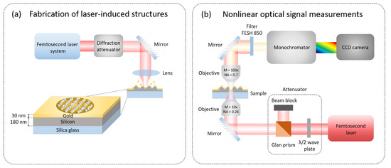
Figure 1.
Outline of the experimental setup. (a) Scheme of laser-induced structures fabrication. The inset shows the structure of gold-silicon bi-layer film supported by glass substrate and illustration of produced structures. (b) Scheme for nonlinear optical signal measurements.
2.2. Fabrication of Laser-Induced Structures
Fabrication of the structures was performed with the use of a commercial femtosecond laser system consisting of a TIF-100-F4 titanium-sapphire laser generator and RAP-1500 regenerative amplifier (Avesta Project Ltd., Moscow, Russia ), which generates laser pulses at the central wavelength of 790 ± 10 nm with a pulse duration of 100 fs and repetition rate of 10 Hz. The pulse energy was controlled by external diffraction attenuator DVA-8-800. Laser pulses with normal incidence to the sample and pulse energy of 9.6 μJ were focused on Au surface in a spot size with a diameter of 60 μm by spherical glass lens (K-8, f = 40 mm, NA ≈ 0.1) (Figure 1a).
2.3. Morphology Measurements
Morphology of laser-induced structures was studied by a combination of a Scanning Electron Microscope (SEM) Neon 40 EsB Crossbeam (Carl Zeiss, Oberkochen, Germany) in a mode of secondary electron detection and by Atomic Force Microscope (AFM) Ntegra Aura (NT-MDT, Moscow, Russia) in semicontact regime by commercially available NSG01 (TipsNano, Tallinn, Estonia) probe.
2.4. Nonlinear Optical Signal Measurements
Nonlinear optical signals were excited via pumping of structures by a Yb-doped solid-state femtosecond oscillator TEMA-150 (Avesta Project, Moscow, Russia) generating at a wavelength of 1050 ± 5 nm, with an output pulse duration of 150 fs and repetition rate of 80 ± 2 MHz (Figure 1b). The average laser power varied in a range of 1-6 mW by attenuator (a Glan prism coupled with a half-wave plate). After passing through the attenuator, a laser beam was focused on the structures from the substrate side by Mitutoyo M Plan APO NIR objective (M = 10 ×, NA = 0.26). Excited SHG and broadband PL signals were collected by Mitutoyo Plan Apo HR objective (100×, NA = 0.70) and sent to spectrometer Horiba LabRam HR800 equipped by a thermoelectrically cooled CCD (Andor DU 420A-OE 325) with a 150-g/mm diffraction grating. The sample was mounted on a piezo stage (AIST NT, Novato, CA, USA), providing positioning accuracy of 10 nm during the two-dimensional mapping of an optical signal.
2.5. Raman Spectroscopy Measurements
A HeNe laser (Thorlabs) with a central wavelength of 632.8 nm and power of 8 mW was used as a pump source for Raman scattering measurements. The laser beam was focused on the sample surface through a Mitutoyo Plan Apo HR objective (100×, NA = 0.7) to spot with a diameter of 1 μm at the 1/e level. The same objective collected a scattered signal, and the light was sent to the spectrometer (HORIBA LabRam HR) with a diffraction grating 1800 lines/mm.
3. Results
3.1. Au-Si Laser-Induced Structures Fabrication and Morphology Characterization
In this work, we used glass-supported bi-layer films composed of 30-nm-thick top Au film and 180-nm-thick bottom Si film. The sample was irradiated by fs-laser pulses with a = 790 nm wavelength. Processing fluence of F = 0.19 J/cm was chosen to be slightly lower than the single-pulse ablation threshold of the top Au layer (F = 0.28 J/cm; [37]). Laser-exposed areas produced upon single-spot irradiation of the sample by varying the number of applied pulses per spot (N = 10, 100, 1000) at fixed fluence are demonstrated in Figure 2a–c. As can be seen on the magnified SEM images (Figure 2e,f), the certain exposed areas within the spot irradiated by a low number of laser pulses (N = 10) contain the nanoparticles arranged along the periodically spaced lines. AFM imaging (inset in Figure 2a,d) supported by 2D-FFT of SEM image (insert in Figure 2e) revealed the averaged periodicity of the lines of about 1.3 μm. Such ordering disappeared at an elevated number of applied pulses per spot N. Also, the density of the nanoparticles decreased from the central part of the exposed spot to its periphery that is generally consistent with the Gaussian-shaped lateral intensity profile of the laser radiation on the sample surface.
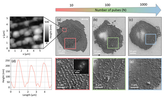
Figure 2.
Characterization of laser-induced hybrid structures topography. (a–c) Top-view SEM images of produced structures after exposure by 10, 100, and 1000 laser pulses, respectively. (d) The profile extracted from the AFM image of structures in (a). (e–g) Corresponding magnified areas of colored boxes from (a–c). Insets show a 3D AFM map of the area which is indicated in (a) as a dashed line red box and a 2D-FFT map of the corresponding SEM image. A white double arrow shows the laser beam polarization direction.
3.2. Au-Si Laser-Induced Structures Nonlinear Photoluminescence
To study nonlinear optical properties of laser-induced hybrid structures, we pumped our structures by femtosecond radiation focused on the spot of 4 μm diameter (corresponding fluence = 0.2 mJ/cm). Figure 3a demonstrates the comparison of PL and second harmonic generation (SHG) from initial film and produced structures. As it can be seen, the initial film produces a weak SHG signal (blue curve), which is observed due to a breaking of inversion symmetry on the surface defects [38]. At the same time, laser-induced structures demonstrate a two orders of magnitude enhancement of produced SHG signal. Moreover, such structures can produce a strong broadband PL signal (green curve). At the next step, to demonstrate the distribution of produced signal along the pattern area, the sample was scanned with respect to laser beam by piezo stage with a step size of 3 μm, and the spectrum was collected at each position. These mapping results are shown in Figure 3b,c, which correspond to SHG and broadband PL signal distribution maps. From a comparison of Figure 3a,b, it can be noticed that the strongest SHG signal is observed from the areas with a higher density of structures (at the edges of a pattern), and similar dependence is found for broadband PL signal (Figure 3b).
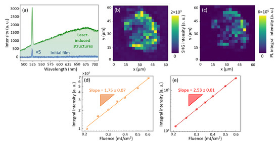
Figure 3.
Nonlinear optical properties of Au-Si laser-induced structures obtained after exposure by 10 laser pulses. (a) Comparison of photoluminescence signal from initial film (blue curve) and laser-induced hybrid structures (green curve). Maps of (b) SHG and (c) broadband PL signals. (d) Dependence of SHG, and (e) broadband PL intensity on pump power.
To investigate the nonlinear signal nature, we recorded a dependence between the pump power and intensity of the produced signal. Dependencies for SHG and broadband PL signals are defined by a set of points and approximated with straight lines, which slopes, in turn, correspond to an order of nonlinear process. For SHG signal dependence (Figure 3d), the slope is equal to 1.75 ± 0.07, which corresponds to the two-photon absorption process. In contrast, for broadband PL signal (Figure 2e), the slope is 2.53 ± 0.01, which evidence of the contribution of both two and three-photon absorption processes [39]. We assume that the primary mechanism of forming a strong broadband PL signal is hot carriers injection from gold to silicon layer, which can significantly enhance the PL signal compared to the signal from pure Si.
3.3. Au-Si Laser-Induced Structures Composition
To trace Si crystallinity changes in created structures compared to the initial sample, we measured Raman scattering signal before and after laser processing. Results of measurements are shown in Figure 4a. The figure shows that the Raman signal for the initial Si film corresponds to the amorphous phase with a broad peak near 480 cm (brown curve). Irradiation of sample by femtosecond laser pulses alongside hybrid structures formation leads to the partial crystallization of silicon with average grain size 5 nm calculated according to the formula (where 2.5 cm is shift of Raman peak compared with peak position for bulk silicon, cm) which is confirmed by a pronounced peak at 517.5 cm (red curve) [40].
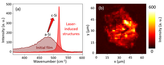
Figure 4.
(a) Comparison of Raman signal from an initial sample (brown curve) and laser-induced surface structures (red curve). (b) Two-dimensional Raman map of fabricated laser-induced structures at a wavenumber of 520 cm.
For a more detailed investigation of composition changes within laser-induced hybrid structures area, we recorded a two-dimensional map of Raman signal with a step size of 1.5 μm where color scale corresponds to an intensity of the signal at the position of a c-Si peak at 520 cm (Figure 4b). From the map, it can be noticed that the strongest signal is observed in the central part of a pattern where irradiation intensity during fabrication achieved a maximum. From the comparison with nonlinear signal maps, it can be concluded that the crystallization of Si film plays an essential role in enhancing SHG and broadband PL signals.
4. Discussion
Ablation/dewetting of nm-thick Au films at bulk silicon or glass substrates is very well studied [41,42,43]. Here we investigate Au-Si bi-layer film supported by a glass substrate under a femtosecond laser exposure. To the best of the authors’ knowledge, a similar system was studied by Datta et al. [44], where 6 nm-thick bi-layer Au-Si films at 300 nm-thick thermally grown SiO on Si undergoes ion irradiation. Therefore, we use much thicker films to manufacture hybrid structures and demonstrate their nonlinear optical response.
Above mentioned observations allow us to suggest the following scenario regarding the formation of such surface morphology. The laser radiation induces the melting of the Au/Si sandwich. The molten layer becomes hydrodynamically unstable, breaking into isolated Au-Si nano-islands or isolated nanoparticles on the glass substrate. According to the performed AFM studies, the height of such isolated nanoparticles can reach 250–500 nm exceeding the total thickness of the Au-Si bi-layer. The formed isolated nanostructures on the thermally insulating substrate underwent multiple melting-resolidification cycles allowing pristine Si material to be transferred from amorphous to nanocrystalline phase that will be discussed somewhat later. Some of the formed nanoparticles can even be acoustically removed from the substrate via relaxation of thermal-generated stress [45]. This correlates with our experimental observations showing a gradually decreasing density of the nanoparticles in the central part of the surface area exposed by elevating several pulses.
The observed laser-induced self-organization of the nanoparticles into periodically arranged lines appears to be driven by hydrodynamics rather than electromagnetic phenomena. First, the lines showed the rather random orientation in the different areas within the entire laser-irradiated spot (Figure 2a). In this respect, the orientation of the periodically arranged lines of nanoparticles does not correlate with the linear polarization direction of the incident laser radiation. Secondly, the measured period of the lines (≈ 1.1–1.5 μm) was found to be larger compared to the incident wavelength ( = 790 nm), while the ordering driven by the interference of the incident light with either the scattered or surface waves suggest the periodicity that is comparable of shorter than . All this suggests that the observed ordering proceeds via laser-induced Rayleigh-like hydrodynamic instability. Additional effects (evaporated material redeposition; non-uniform heating due to Gaussian distribution of laser intensity across the focal spot together with differences in thermal properties of gold, silicon, and glass substrate; features of surface diffusion and hydrodynamic flow in such complex system) could affect. Therefore, we assume that for nm-thick films, the maximum height of produced structures is about the double total thickness of bi-layers, which was confirmed by AFM measurements.
It is known that enhancement of SHG in small metallic and dielectric particles may come due to the increased surface effect. For laser-printed silicon nanoparticles, it was shown that the main contribution to the enhancement of SHG comes from the local breaking of inversion symmetry on interfaces between Si grains which are formed under laser irradiation [46]. For hybrid Au-Si nanoparticles excitation of broadband PL is based on hot carriers injection after two and three-photon absorption processes [8]. Here we develop laser-induced hybrid structures by femtosecond laser writing on gold-silicon bi-layer film alternatively to laser printing mentioned above and extensively used to produce nanoparticles from single-layer films [47]. It should be noted that silicon crystallization takes place both under laser printing of nanoparticles [48] and femtosecond laser exposure [49] used here as confirmed by Raman measurements.
The repeatability of the proposed technique is mainly limited by the pulse-to-pulse stability of the laser source, careful adjustment of processing setup, and the quality of the initial bi-layer film since any film defects will affect the final structures.
5. Conclusions
We have developed laser-induced hybrid structures after exposure of gold-silicon bi-layer film (thicknesses of 30 nm and 180 nm, correspondingly) by femtosecond laser pulses ( = 790 nm). Obtained laser-induced hybrid structures have an average period of about 1.3 μm, and the typical height is ∼200–500 nm. We demonstrated that such structures could enhance SHG signal up to 500 times and emit broadband photoluminescence. This can be attributed to hot carriers injection from gold to silicon, where silicon crystallinity is crucial for enhancing SHG and broadband PL signals. Raman scattering measurements confirm silicon crystallization during the formation of structures. Moreover, such hybrid structures provide broadband PL (white light) and can be a useful tool for spectroscopy, the broadband near-field sounding of nanophotonic devices, or mapping their optical properties due to fabrication flexibility and strong nonlinear optical properties. In terms of device applications, such hybrid nano-islands are attractive for optical biosensing and the development of nanophotonic devices based on broadband photoluminescence.
Author Contributions
Conceptualization, E.P., E.A. and D.Z.; methodology, E.A., F.K. and V.V.; software, E.P.; validation, E.A., A.K. and D.Z.; formal analysis, D.Z.; investigation, E.P., E.A. and F.K.; resources, D.K, I.M. and V.V.; data curation, D.Z. and A.K.; writing—original draft preparation, E.P., E.A., S.K., D.K., I.M., A.K. and D.Z.; writing—review and editing, E.A. and S.K.; visualization, E.P.; supervision, D.Z.; project administration, E.A.; funding acquisition, E.A. All authors have read and agreed to the published version of the manuscript.
Funding
This research was funded by the Russian Science Foundation (Project 19-79-10259).
Data Availability Statement
The data that support the findings of this study are available from the corresponding author upon reasonable request.
Acknowledgments
The authors are grateful to Dmitriy M. Dolgintsev for AFM measurements.
Conflicts of Interest
The authors declare no conflict of interest.
References
- Sugimoto, H.; Fujii, M. Broadband dielectric–metal hybrid nanoantenna: Silicon nanoparticle on a mirror. ACS Photonics 2018, 5, 1986–1993. [Google Scholar] [CrossRef]
- Dudek, M.; Kowerdziej, R.; Pianelli, A.; Parka, J. Graphene-based tunable hyperbolic microcavity. Sci. Rep. 2021, 11, 1–11. [Google Scholar] [CrossRef] [PubMed]
- Pan, L.; Liu, Y.T.; Zhong, M.; Xie, X.M. Coordination-Driven Hierarchical Assembly of Hybrid Nanostructures Based on 2D Materials. Small 2020, 16, 1902779. [Google Scholar] [CrossRef] [PubMed]
- Shibanuma, T.; Grinblat, G.; Albella, P.; Maier, S.A. Efficient third harmonic generation from metal–dielectric hybrid nanoantennas. Nano Lett. 2017, 17, 2647–2651. [Google Scholar] [CrossRef]
- Falamas, A.; Tosa, V.; Farcau, C. Hybrid architectures made of nonlinear-active and metal nanostructures for plasmon-enhanced harmonic generation. Opt. Mater. 2019, 88, 653–666. [Google Scholar] [CrossRef]
- Sun, S.; Zhang, T.; Liu, Q.; Ma, L.; Du, Q.; Duan, H. Enhanced directional fluorescence emission of randomly oriented emitters via a metal–dielectric hybrid nanoantenna. J. Phys. Chem. C 2019, 123, 21150–21160. [Google Scholar] [CrossRef]
- Athanasiou, C.E.; Bellouard, Y. A monolithic micro-tensile tester for investigating silicon dioxide polymorph micromechanics, fabricated and operated using a femtosecond laser. Micromachines 2015, 6, 1365–1386. [Google Scholar] [CrossRef]
- Makarov, S.; Sinev, I.; Milichko, V.; Komissarenko, F.; Zuev, D.; Ushakova, E.; Mukhin, I.; Yu, Y.; Kuznetsov, A.; Belov, P.; et al. Nanoscale generation of white light for ultrabroadband nanospectroscopy. Nano Lett. 2018, 18, 535–539. [Google Scholar] [CrossRef]
- Larin, A.; Nominé, A.; Ageev, E.; Ghanbaja, J.; Kolotova, L.; Starikov, S.; Bruyère, S.; Belmonte, T.; Makarov, S.; Zuev, D. Plasmonic nanosponges filled with silicon for enhanced white light emission. Nanoscale 2020, 12, 1013–1021. [Google Scholar] [CrossRef]
- Andreeva, Y.; Sharma, N.; Rudenko, A.; Mikhailova, J.; Sergeev, M.; Veiko, V.P.; Vocanson, F.; Lefkir, Y.; Destouches, N.; Itina, T.E. Insights into Ultrashort Laser-Driven Au: TiO2 Nanocomposite Formation. J. Phys. Chem. C 2020, 124, 10209–10219. [Google Scholar] [CrossRef]
- Mintcheva, N.; Srinivasan, P.; Rayappan, J.B.B.; Kuchmizhak, A.A.; Gurbatov, S.; Kulinich, S.A. Room-temperature gas sensing of laser-modified anatase TiO2 decorated with Au nanoparticles. Appl. Surf. Sci. 2020, 507, 145169. [Google Scholar] [CrossRef]
- Gurbatov, S.O.; Modin, E.; Puzikov, V.; Tonkaev, P.; Storozhenko, D.; Sergeev, A.; Mintcheva, N.; Yamaguchi, S.; Tarasenka, N.N.; Chuvilin, A.; et al. Black Au-Decorated TiO2 Produced via Laser Ablation in Liquid. ACS Appl. Mater. Interfaces 2021, 13, 6522. [Google Scholar] [CrossRef] [PubMed]
- Beresna, M.; Gecevičius, M.; Kazansky, P.G.; Gertus, T. Radially polarized optical vortex converter created by femtosecond laser nanostructuring of glass. Appl. Phys. Lett. 2011, 98, 201101. [Google Scholar] [CrossRef]
- Vlugter, P.; Bellouard, Y. Elastic properties of self-organized nanogratings produced by femtosecond laser exposure of fused silica. Phys. Rev. Mater. 2020, 4, 023607. [Google Scholar] [CrossRef]
- Bonse, J.; Kirner, S.V.; Höhm, S.; Epperlein, N.; Spaltmann, D.; Rosenfeld, A.; Krüger, J. Applications of laser-induced periodic surface structures (LIPSS). In Proceedings of the SPIE Photonics West Conference 2017, Laser-Based Micro- and Nanoprocessing XI, San Francisco, CA, USA, 28 January–2 February 2017; Volume 10092, p. 100920N. [Google Scholar]
- Müller, F.A.; Kunz, C.; Gräf, S. Bio-inspired functional surfaces based on laser-induced periodic surface structures. Materials 2016, 9, 476. [Google Scholar] [CrossRef]
- Baron, C.F.; Mimidis, A.; Puerto, D.; Skoulas, E.; Stratakis, E.; Solis, J.; Siegel, J. Biomimetic surface structures in steel fabricated with femtosecond laser pulses: Influence of laser rescanning on morphology and wettability. Beilstein J. Nanotechnol. 2018, 9, 2802–2812. [Google Scholar] [CrossRef] [PubMed]
- Bonse, J.; Kirner, S.V.; Krüger, J. Laser-induced periodic surface structures (LIPSS). In Handbook of Laser Micro- and Nano-Engineering; Springer International Publishing: Cham, Switzerland, 2020; pp. 1–59. [Google Scholar]
- Bonse, J.; Gräf, S. Maxwell Meets Marangoni—A Review of Theories on Laser-Induced Periodic Surface Structures. Laser Photonics Rev. 2020, 14, 2000215. [Google Scholar] [CrossRef]
- Vorobyev, A.; Makin, V.; Guo, C. Periodic ordering of random surface nanostructures induced by femtosecond laser pulses on metals. J. Appl. Phys. 2007, 101, 034903. [Google Scholar] [CrossRef]
- Bonse, J.; Krüger, J.; Höhm, S.; Rosenfeld, A. Femtosecond laser-induced periodic surface structures. J. Laser Appl. 2012, 24, 042006. [Google Scholar] [CrossRef]
- Dostovalov, A.; Bronnikov, K.; Korolkov, V.; Babin, S.; Mitsai, E.; Mironenko, A.; Tutov, M.; Zhang, D.; Sugioka, K.; Maksimovic, J.; et al. Hierarchical anti-reflective laser-induced periodic surface structures (LIPSSs) on amorphous si films for sensing applications. Nanoscale 2020, 12, 13431–13441. [Google Scholar] [CrossRef]
- Costache, F.; Kouteva-Arguirova, S.; Reif, J. Sub–damage–threshold femtosecond laser ablation from crystalline Si: Surface nanostructures and phase transformation. Appl. Phys. A 2004, 79, 1429–1432. [Google Scholar] [CrossRef]
- Shen, M.; Carey, J.E.; Crouch, C.H.; Kandyla, M.; Stone, H.A.; Mazur, E. High-density regular arrays of nanometer-scale rods formed on silicon surfaces via femtosecond laser irradiation in water. Nano Lett. 2008, 8, 2087–2091. [Google Scholar] [CrossRef]
- Makarov, S.; Tsypkin, A.; Voytova, T.; Milichko, V.; Mukhin, I.; Yulin, A.; Putilin, S.; Baranov, M.; Krasnok, A.; Morozov, I.; et al. Self-adjusted all-dielectric metasurfaces for deep ultraviolet femtosecond pulse generation. Nanoscale 2016, 8, 17809–17814. [Google Scholar] [CrossRef]
- Trice, J.; Thomas, D.; Favazza, C.; Sureshkumar, R.; Kalyanaraman, R. Pulsed-laser-induced dewetting in nanoscopic metal films: Theory and experiments. Phys. Rev. B 2007, 75, 235439. [Google Scholar] [CrossRef]
- Ye, J.; Zuev, D.; Makarov, S. Dewetting mechanisms and their exploitation for the large-scale fabrication of advanced nanophotonic systems. Int. Mater. Rev. 2019, 64, 439–477. [Google Scholar] [CrossRef]
- Ruffino, F.; Grimaldi, M.G. Nanostructuration of thin metal films by pulsed laser irradiations: A review. Nanomaterials 2019, 9, 1133. [Google Scholar] [CrossRef]
- Berzins, J.; Indrisiunas, S.; Van Erve, K.; Nagarajan, A.; Fasold, S.; Steinert, M.; Gerini, G.; Gecys, P.; Pertsch, T.; Baumer, S.M.; et al. Direct and high-throughput fabrication of Mie-resonant metasurfaces via single-pulse laser interference. ACS Nano 2020, 14, 6138–6149. [Google Scholar] [CrossRef] [PubMed]
- Ruffino, F.; Grimaldi, M.G. Controlled dewetting as fabrication and patterning strategy for metal nanostructures. Phys. Status Solidi (a) 2015, 212, 1662–1684. [Google Scholar] [CrossRef]
- Bischof, J.; Scherer, D.; Herminghaus, S.; Leiderer, P. Dewetting modes of thin metallic films: Nucleation of holes and spinodal dewetting. Phys. Rev. Lett. 1996, 77, 1536. [Google Scholar] [CrossRef] [PubMed]
- Fowlkes, J.D.; Kondic, L.; Diez, J.; Wu, Y.; Rack, P.D. Self-assembly versus directed assembly of nanoparticles via pulsed laser induced dewetting of patterned metal films. Nano Lett. 2011, 11, 2478–2485. [Google Scholar] [CrossRef]
- Makarov, S.V.; Milichko, V.A.; Mukhin, I.S.; Shishkin, I.I.; Zuev, D.A.; Mozharov, A.M.; Krasnok, A.E.; Belov, P.A. Controllable femtosecond laser-induced dewetting for plasmonic applications. Laser Photonics Rev. 2016, 10, 91–99. [Google Scholar] [CrossRef]
- Zuev, D.A.; Makarov, S.V.; Mukhin, I.S.; Milichko, V.A.; Starikov, S.V.; Morozov, I.A.; Shishkin, I.I.; Krasnok, A.E.; Belov, P.A. Fabrication of Hybrid Nanostructures via Nanoscale Laser-Induced Reshaping for Advanced Light Manipulation. Adv. Mater. 2016, 28, 3087–3093. [Google Scholar] [CrossRef] [PubMed]
- Dmitriev, P.; Makarov, S.; Milichko, V.; Mukhin, I.; Gudovskikh, A.; Sitnikova, A.; Samusev, A.; Krasnok, A.; Belov, P. Laser fabrication of crystalline silicon nanoresonators from an amorphous film for low-loss all-dielectric nanophotonics. Nanoscale 2016, 8, 5043–5048. [Google Scholar] [CrossRef] [PubMed]
- Wang, D.; Schaaf, P. Nanoporous gold nanoparticles. J. Mater. Chem. 2012, 22, 5344–5348. [Google Scholar] [CrossRef]
- Wang, X.; Kuchmizhak, A.; Li, X.; Juodkazis, S.; Vitrik, O.; Kulchin, Y.N.; Zhakhovsky, V.; Danilov, P.; Ionin, A.; Kudryashov, S.; et al. Laser-induced translative hydrodynamic mass snapshots: Noninvasive characterization and predictive modeling via mapping at nanoscale. Phys. Rev. Appl. 2017, 8, 044016. [Google Scholar] [CrossRef]
- Gielis, J.; Gevers, P.; Aarts, I.; Van De Sanden, M.; Kessels, W. Optical second-harmonic generation in thin film systems. J. Vac. Sci. Technol. A: Vacuum, Surfaces, Film. 2008, 26, 1519–1537. [Google Scholar] [CrossRef]
- Zhang, C.; Xu, Y.; Liu, J.; Li, J.; Xiang, J.; Li, H.; Li, J.; Dai, Q.; Lan, S.; Miroshnichenko, A.E. Lighting up silicon nanoparticles with Mie resonances. Nat. Commun. 2018, 9, 1–7. [Google Scholar] [CrossRef]
- He, Y.; Yin, C.; Cheng, G.; Wang, L.; Liu, X.; Hu, G. The structure and properties of nanosize crystalline silicon films. J. Appl. Phys. 1994, 75, 797–803. [Google Scholar] [CrossRef]
- Koch, J.; Korte, F.; Bauer, T.; Fallnich, C.; Ostendorf, A.; Chichkov, B. Nanotexturing of gold films by femtosecond laser-induced melt dynamics. Appl. Phys. A 2005, 81, 325–328. [Google Scholar] [CrossRef]
- Kuznetsov, A.; Koch, J.; Chichkov, B. Nanostructuring of thin gold films by femtosecond lasers. Appl. Phys. A 2009, 94, 221–230. [Google Scholar] [CrossRef]
- Kuznetsov, A.I.; Unger, C.; Koch, J.; Chichkov, B.N. Laser-induced jet formation and droplet ejection from thin metal films. Appl. Phys. A 2012, 106, 479–487. [Google Scholar] [CrossRef]
- Datta, D.; Siva, V.; Varma, S.; Kanjilal, D.; Sahoo, P. Ion induced dewetting of Au–Si on a SiO2 surface: Composite nanodot evolution and wettability transition. Phys. Chem. Chem. Phys. 2016, 18, 29955–29960. [Google Scholar] [CrossRef]
- Zhigilei, L.V.; Garrison, B.J. Microscopic mechanisms of laser ablation of organic solids in the thermal and stress confinement irradiation regimes. J. Appl. Phys. 2000, 88, 1281–1298. [Google Scholar] [CrossRef]
- Makarov, S.V.; Petrov, M.I.; Zywietz, U.; Milichko, V.; Zuev, D.; Lopanitsyna, N.; Kuksin, A.; Mukhin, I.; Zograf, G.; Ubyivovk, E.; et al. Efficient second-harmonic generation in nanocrystalline silicon nanoparticles. Nano Lett. 2017, 17, 3047–3053. [Google Scholar] [CrossRef]
- Zhigunov, D.M.; Evlyukhin, A.B.; Shalin, A.S.; Zywietz, U.; Chichkov, B.N. Femtosecond laser printing of single Ge and SiGe nanoparticles with electric and magnetic optical resonances. ACS Photonics 2018, 5, 977–983. [Google Scholar] [CrossRef]
- Zywietz, U.; Evlyukhin, A.B.; Reinhardt, C.; Chichkov, B.N. Laser printing of silicon nanoparticles with resonant optical electric and magnetic responses. Nat. Commun. 2014, 5, 1–7. [Google Scholar] [CrossRef]
- Choi, T.Y.; Hwang, D.J.; Grigoropoulos, C.P. Ultrafast laser-induced crystallization of amorphous silicon films. Opt. Eng. 2003, 42, 3383–3388. [Google Scholar]


Publisher’s Note: MDPI stays neutral with regard to jurisdictional claims in published maps and institutional affiliations. |
© 2021 by the authors. Licensee MDPI, Basel, Switzerland. This article is an open access article distributed under the terms and conditions of the Creative Commons Attribution (CC BY) license (https://creativecommons.org/licenses/by/4.0/).