Development of Micron Sized Photonic Devices Based on Deep GaN Etching


Abstract
1. Introduction
2. Experimental Details
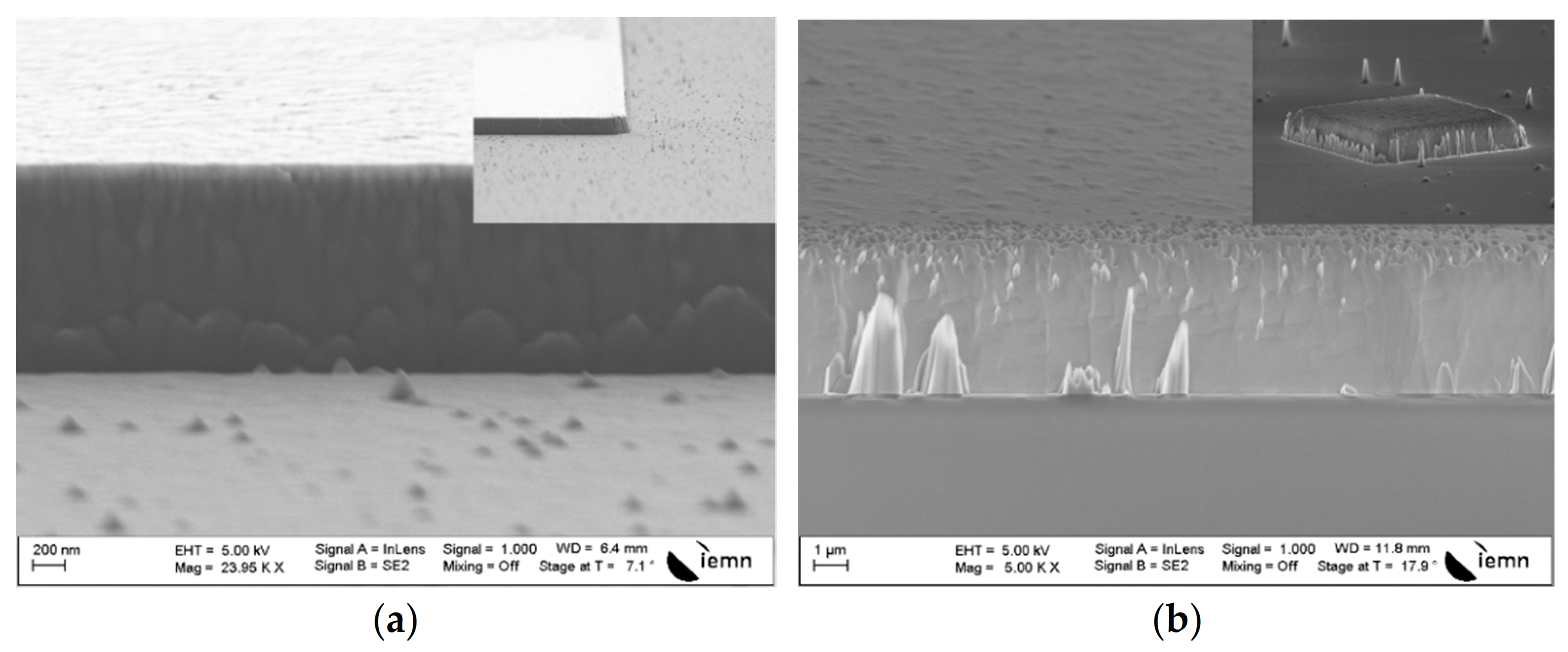
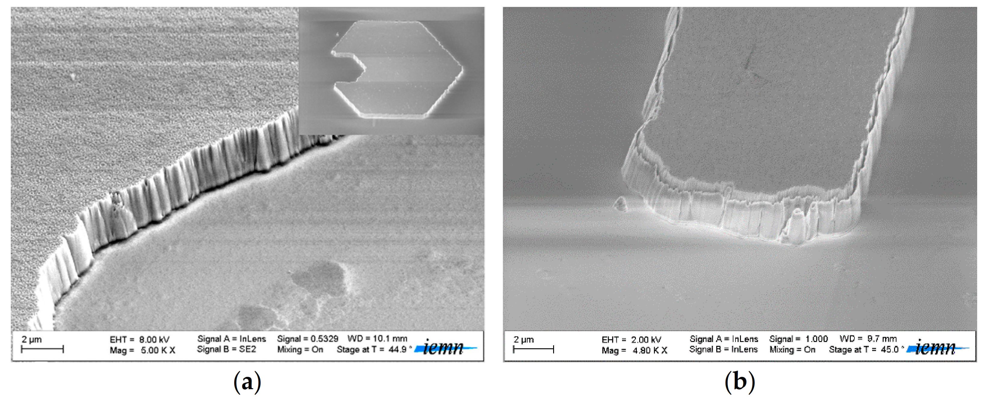
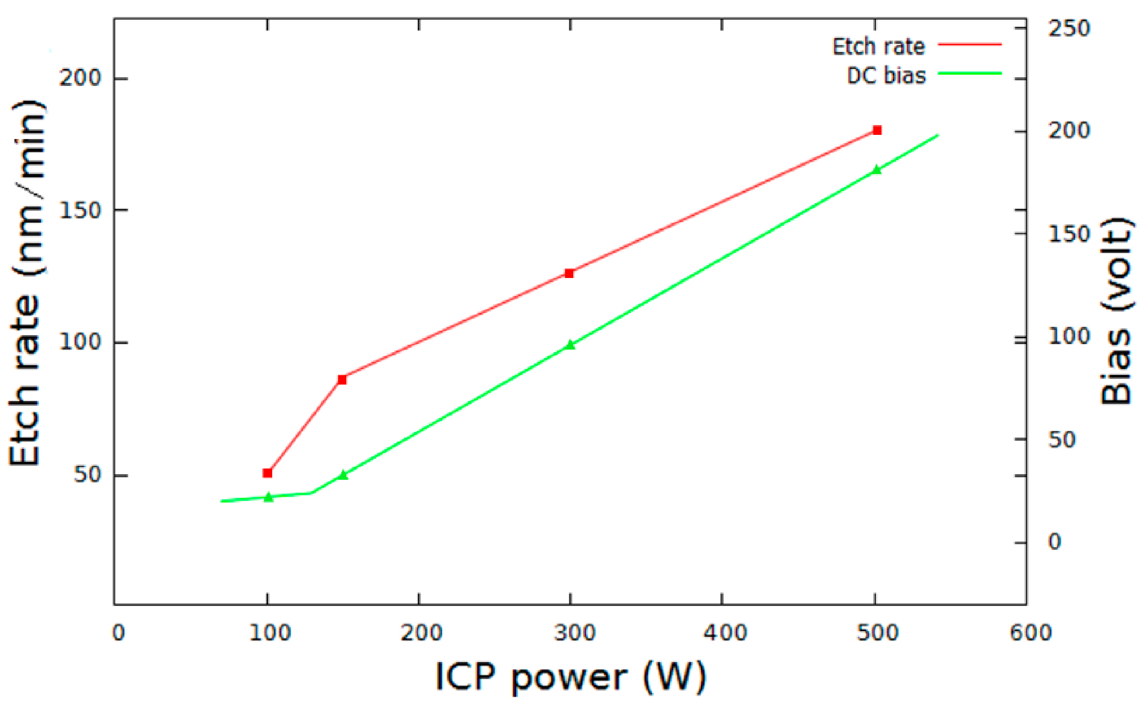
3. Results and Discussion
4. Conclusions
Author Contributions
Funding
Data Availability Statement
Acknowledgments
Conflicts of Interest
References
- Li, X.; Jiang, Y.; Li, J.; Shi, Z.; Zhu, G.; Wang, Y. Integrated photonics chip with InGaN/GaN light-emitting diode and bended waveguide for visible-light communicacations. Opt. Laser Technol. 2019, 114, 103–109. [Google Scholar] [CrossRef]
- Zhou, S.; Wang, S.; Liu, S.; Ding, H. High power GaN-based LEDs with low optical loss electrode structure. Opt. Laser Technol. 2013, 54, 321–325. [Google Scholar] [CrossRef]
- Li, K.H.; Fu, W.Y.; Cheung, Y.F.; Wong, K.K.Y.; Wang, Y.; Lau, K.M.; Choi, H.W. Monolithically integrated InGaN/GaN light-emitting diodes, photodetectors, and waveguides on Si substrate. Optica 2018, 5, 564. [Google Scholar] [CrossRef]
- Nakamura, S. InGaN-Based laser diodes. Annu. Rev. Mater. Sci. 1998, 28, 125–152. [Google Scholar] [CrossRef]
- Omnès, F.; Monroy, E.; Muñoz, E.; Reverchon, J.-L. Wide bandgap UV photodetectors: A short review of devices and applications. SPIE 2007, 6473, 64730E. [Google Scholar]
- Lee, K.H.; Joo, D.H.; Kim, M.S.; Yu, J.S. Improved light extraction of InGaN/GaN blue LEDs by GaOOH NRAs using a thin ATO seed layer. Nanoscale Res. Lett. 2012, 7, 458. [Google Scholar] [CrossRef]
- Khokhar, A.Z.; Parsons, K.; Hubbard, G.; Rahman, F.; Macintyre, D.S.; Xiong, C.; Massoubre, D.; Gong, Z.; Johnson, N.P.; De La Rue, R.M.; et al. Nanofabrication of gallium nitride photonic crystal light-emitting diodes. Microelectron. Eng. 2010, 87, 2200–2207. [Google Scholar] [CrossRef][Green Version]
- Hong, S.; Cho, C.; Lee, S.; Yim, S.; Lim, W.; Kim, S.; Park, S. Localized surface plasmon-enhanced near-ultraviolet emission from InGaN/GaN light-emitting diodes using silver and platinum nanoparticles. Opt. Express 2013, 21, 3138–3144. [Google Scholar] [CrossRef] [PubMed]
- Baik, K.H.; Pearton, S.J. Dry etching characteristics of GaN for blue/green light-emitting diode fabrication. Appl. Surf. Sci. 2009, 255, 5948–5951. [Google Scholar] [CrossRef]
- Zhang, Y.; Sun, M.; Piedra, D.; Azize, M.; Zhang, X.; Fujishima, T.; Palacios, T. GaN-on-Si vertical schottky and p-n diodes. IEEE Electron. Dev. Lett. 2014, 35, 618–620. [Google Scholar]
- Hu, J.; Zhang, Y.; Sun, M.; Piedra, D.; Chowdhury, N.; Palacios, T. Materials and processing issues in vertical GaN power electronics. Mater. Sci. Semicond. Proc. 2018, 78, 75–84. [Google Scholar] [CrossRef]
- Tohru, O. Recent development of vertical GaN power devices: Japanese. J. Appl. Phys. 2019, 58, SB0805. [Google Scholar]
- Xiao, M.; Yan, X.; Xie, J.; Beam, E.; Cao, Y.; Wang, H.; Zhang, Y. Origin of leakage current in vertical GaN devices with nonplanar regrown p-GaN. Appl. Phys. Lett. 2020, 117, 183502. [Google Scholar] [CrossRef]
- Sun, Y.; Kang, X.; Zheng, Y.; Lu, J.; Tian, X.; Wei, K.; Wu, H.; Wang, W.; Liu, X.; Zhang, G. Review of the Recent Progress on GaN-Based Vertical Power Schottky Barrier Diodes (SBDs). Electronics 2019, 8, 575. [Google Scholar] [CrossRef]
- Hsieh, Y.; Chen, W.; Chang, L.; Chow, L.; Borges, S.; Schulte, J.A.; Huang, S.; Jeng, M.; Yu, C. Etched Gallium Nitride Waveguide for RamanSpectroscopic Applications. Crystals 2019, 9, 176. [Google Scholar] [CrossRef]
- Qiu, R.; Lu, H.; Chen, D.; Zhang, R.; Zheng, Y. Optimization of inductively coupled plasma deep etching of GaN and etching damage analysis. Appl. Surf. Sci. 2011, 257, 2700. [Google Scholar] [CrossRef]
- le Boulbar, E.D.; Lewins, C.J.; Allsopp, D.W.E.; Bowen, C.R.; Shields, P.A. Fabrication of high-aspect ratio GaN nanostructures nanostructures for advanced photonic devices. Microelectron. Eng. 2016, 153, 132–136. [Google Scholar] [CrossRef]
- Okada, N.; Nojima, K.; Ishibashi, N.; Nagatoshi, K.; Itagaki, N.; Inomoto, R.; Motoyama, S.; Kobayashi, T.; Tadatomo, K. Formation of distinctive structures of GaN by inductively-coupled-plasma and reactive ion etching under optimized chemical etching conditions. AIP Adv. 2017, 7, 065111. [Google Scholar] [CrossRef]
- Jeon, C.W.; Choi, H.W.; Dawson, M.D. Fabrication of Matrix-Addressable InGaN-Based Microdisplays of High Array Density. IEEE Photonics Technol. Lett. 2003, 15, 1516–1518. [Google Scholar] [CrossRef]
- Wu, X.H.; Elsass, C.R.; Abare, A.; MacK, M.; Keller, S.; Petroff, P.M.; Denbaars, S.P.; Speck, J.S.; Rosner, S.J. Structural origin of V-defects and correlation with localized excitonic centers in InGaN/GaN multiple quantum wells. Appl. Phys. Lett. 1998, 72, 692–694. [Google Scholar] [CrossRef]
- Lester, S.D.; Ponce, F.A.; Craford, M.G.; Steigerwald, D.A. High dislocation densities in high efficiency GaN-based light-emitting diodes. Appl. Phys. Lett. 1995, 66, 1249–1251. [Google Scholar] [CrossRef]
- Kim, I.H.; Park, H.S.; Park, Y.J.; Kim, T. Formation of V-shaped pits in InGaN/GaN multiquantum wells and bulk InGaN films. Appl. Phys. Lett. 1998, 73, 1634–1636. [Google Scholar] [CrossRef]
- Yang, G.F.; Chen, P.; Wu, Z.L.; Yu, Z.G.; Zhao, H.; Liu, B.; Hua, X.M.; Xie, Z.L.; Xiu, X.Q.; Han, P. Characteristics of GaN thin films by inductively coupled plasma etching with Cl2/BCl3 and Cl2/Ar. J. Mater. Sci. Mater. Electron. 2012, 23, 1224–1228. [Google Scholar] [CrossRef]
- Cho, H.; Hahn, Y.B.; Hays, D.C.; Jung, K.B.; Donovan, S.M.; Abernathy, C.R.; Pearton, S.J.; Shul, R.J. Inductively Coupled Plasma Etching of III-Nitrides in Cl2/Xe, Cl2/Ar and Cl2/He. Mater. Res. Soc. Internet J. Nitride Semicond. Res. 1999, 4, 763–768. [Google Scholar] [CrossRef][Green Version]
- Rawal, D.; Arora, H.; Sehgal, B.; Muralidharan, R. Comparative study of GaN mesa etch characteristics in Cl2 based inductively coupled plasma with Ar and BCl3 as additive gases. J. Vacuum Sci. Technol. A 2014, 32, 031301. [Google Scholar] [CrossRef]
- Kim, H.K.; Lin, H.; Ra, Y. Etching mechanism of a GaN/InGaN/GaN heterostructure in Cl2 and CH4 based inductively coupled plasmas. J. Vac. Sci. Technol. A 2004, 22, 598–601. [Google Scholar] [CrossRef]
- Lai, Y.; Yeh, C.; Wang, J.; Wang, H.H.; Chen, C.; Hung, W. Sputtering and Etching of GaN Surfaces. J. Phys. Chem. B 2001, 105, 10029–10036. [Google Scholar] [CrossRef]
- Ladroue, J.; Meritan, A.; Boufnichel, M.; Lefaucheux, P.; Ranson, P.; Dussart, R. Deep GaN etching by inductively coupled plasma and induced surface defects. J. Vac. Sci. Technol. A 2010, 28, 1226. [Google Scholar] [CrossRef]
- Evgeny, Z.; Sergei, S.; Alan, G.; Wang, W.N.; Shreter, Y.G.; Tarkhin, D.V.; Bochkareva, N.I. ICP etching of III-nitride based laser structure with Cl2–Ar plasma assisted by Si coverplate material. J. Vac. Sci. Technol. A 2005, 23, 687–692. [Google Scholar]
- Lee, H.; Harris, J. Iron nitride mask and reactive ion etching of GaN films. J. Electron. Mater. 1998, 27, 185–189. [Google Scholar] [CrossRef]


Publisher’s Note: MDPI stays neutral with regard to jurisdictional claims in published maps and institutional affiliations. |
© 2021 by the authors. Licensee MDPI, Basel, Switzerland. This article is an open access article distributed under the terms and conditions of the Creative Commons Attribution (CC BY) license (http://creativecommons.org/licenses/by/4.0/).
Share and Cite
Dogheche, K.; Alshehri, B.; Patriache, G.; Dogheche, E. Development of Micron Sized Photonic Devices Based on Deep GaN Etching. Photonics 2021, 8, 68. https://doi.org/10.3390/photonics8030068
Dogheche K, Alshehri B, Patriache G, Dogheche E. Development of Micron Sized Photonic Devices Based on Deep GaN Etching. Photonics. 2021; 8(3):68. https://doi.org/10.3390/photonics8030068
Chicago/Turabian StyleDogheche, Karim, Bandar Alshehri, Galles Patriache, and Elhadj Dogheche. 2021. "Development of Micron Sized Photonic Devices Based on Deep GaN Etching" Photonics 8, no. 3: 68. https://doi.org/10.3390/photonics8030068
APA StyleDogheche, K., Alshehri, B., Patriache, G., & Dogheche, E. (2021). Development of Micron Sized Photonic Devices Based on Deep GaN Etching. Photonics, 8(3), 68. https://doi.org/10.3390/photonics8030068