Abstract
Versatile applications call for InGaN-based light-emitting diodes (LEDs) to operate at ultra-high current densities with high quantum efficiency. In this work, we investigated the size-dependent effects of the electrical and optical performance of LEDs as increasing the current density up to 100 A/cm2, which demonstrated that mini-strip flip-chip LEDs were superior option to achieve better performance. In detail, at a current density of 100 A/cm2, the light output power density of these mini-strip LEDs was improved by about 6.1 W/cm2, leading to an improvement in the wall-plug efficiency by 4.23%, while the operating temperature was reduced by 11.3 °C, as compared with the large-sized LEDs. This could be attributed to the increase in the sidewall light extraction, alleviated current crowding effect, and improved heat dissipation. This work suggests an array of mini-strip LEDs would provide an option in achieving higher luminescent efficiency at ultrahigh current injection conditions for various applications.
1. Introduction
InGaN-based light-emitting diodes (LEDs) have emerged as vital building blocks in widespread applications like solid-state lighting [1,2,3], displays [4,5,6,7], and visible light communications [8,9,10]. Tremendous progress has been made in the past few years, whereby high quantum efficiency LEDs have been achieved in both blue and green ranges [11,12]. However, there is still much room for improvement in the performance of LEDs as driven at high current densities. Under high current injection densities, the external quantum efficiency (EQE) of LEDs will drop sharply, which is the so-called droop effect. Although still under debate, mechanisms leading to efficiency droop have been mainly identified to be Auger recombination [13,14,15], active region effect [16,17], carrier localization [18,19,20], and carrier leakage [21,22,23]. In addition, the reduction in LED efficiency at high current injection conditions will cause serious thermal problems, which would remarkably affect LED reliability and its lifetime [24,25]. In terms of material growth, a series of remedial measures to tackle efficiency droop have been taken, which mainly focus on (a) reducing the carrier densities in the quantum wells [26], (b) improving the electron confinement within the active region [17,27], or (c) enhancing the hole injection [28]. In the device aspect, effective solutions have concurrently been proposed to deal with the efficiency droop. One way is to transfer the GaN thin-films epitaxially grown on sapphire to a substrate with good thermal conductivity via wafer bonding, which would reduce the LED operating temperature or junction temperature, thereby increasing the output power [29,30,31,32]. This technical route has certain drawbacks, in which the yield and the costs during the production are the leading ones, as the sapphire substrates need to be removed by a laser lift-off process that would induce damages to the thin-films transferred. Another technical route is to use ultra-large mesa thin-film LEDs (usually in several mm2 scale), which aims to push the working current density to the lower end, where the droop effect could be significantly alleviated, in order to achieve higher quantum efficiency even at high current injection conditions [33,34]. However, with this method, the mesa size must be so greatly enlarged that it will induce severe current crowding effect, particularly on the p-side, leading to a degradation in both internal quantum efficiency and light extraction efficiency [35,36]. Recently, micro-LED (µ-LED) technology has been developing rapidly as it has great potentials in next-generation displays and widespread applications, yet there are still existing great challenges for µ-LEDs to achieve high efficiency due to severe Shockley-Hall-Read (SHR) recombination and surface recombination processes. They are also faced with difficulties in the way of electrical interconnects for each component [6,37,38,39].
In this work, the size-dependent electrical, optical, and thermal properties of the flip-chip mini-LEDs are studied at the current density approaching 100 A/cm2. Our results show that mini-strip LEDs exhibit more uniform light emission, greater light emission power density, higher wall-plug efficiency (WPE), and lower junction temperature, which suggests the use of mini-strip LED arrays as light sources would provide an option for achieving high quantum efficiency, which is more suitable especially at high current injection conditions.
2. Experiment
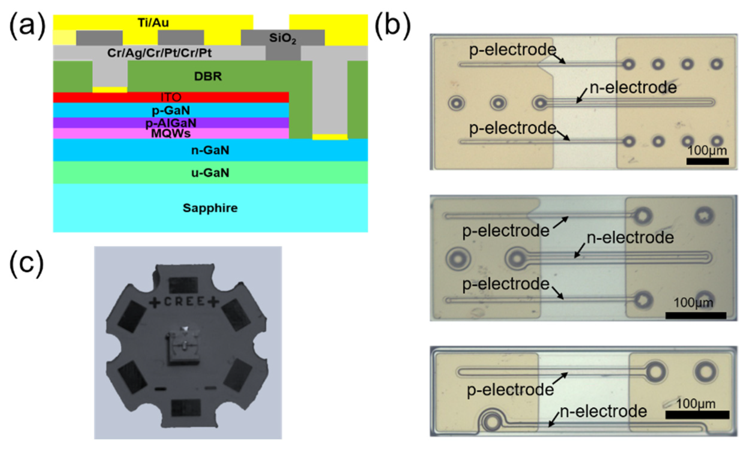
The epitaxial layers for the mini-strip LEDs in this study were grown on 4-inch patterned sapphire substrates (PSS) by MOCVD, with an emission wavelength centered at ~450 nm. In detail, the epitaxial structure consisted of a layer of GaN buffer, a layer of 3.5 µm un-doped GaN, a layer of 2 µm Si-doped (~2.5 × 1019 cm−3) n-GaN, followed by 0.135 µm InGaN/GaN multiple quantum wells (MQWs), a 0.02 µm p-Al0.1Ga0.9N electron blocking layer (EBL), and a layer of 0.08 µm Mg-doped (~3.6 × 1019 cm−3) p-GaN. The InGaN/GaN MQWs were composed of 9 periods each with a 3.5 nm In0.17Ga0.83N well and a 10 nm GaN barrier. As to device processing, indium tin oxide (ITO) with a thickness of 100 nm was used as the current spreading layer and annealed at 550 °C in nitrogen for 30 min. For the device mesa definition, an inductively coupled plasma (ICP) etching process was carried out to a depth as n-GaN was exposed after the above ITO was etched away. Here, to investigate the size-dependent effect, LED chips with three dimensions of 15 × 30 mil2 (Type-I), 10 × 21 mil2 (Type-II), and 06 × 20 mil2 (Type-III) were fabricated (1 mil ≈ 25.4 µm). Ti/Au (50/200 nm) layers were deposited on n-GaN by electron beam evaporation as n-contacts. A total of 5 pairs of TiO2/SiO2 (46.4/76.8 nm) distributed Bragg reflectors (DBR) were deposited, and windows were opened on the p-/n- electrodes by ICP etching. Again, a metallic reflector consisting of Cr/Ag/Cr/Pt/Cr (1/150/20/20/60 nm) was deposited and annealed at 500 °C in N2 for 6 min. Afterwards, 1 µm SiO2 was deposited on the metallic reflector to realize the electrical isolation between the p- and n- electrodes. An extra layer of thick Ti/Au was deposited as metal pads for flip-chip mounting. The schematic structure and cross-sectional image of a mini-strip LED is shown in Figure 1a. Finally, a laser-scribing process was used to separate the wafer into independent LED chips, as shown in Figure 1b. For the testing, we used solder paste as the adhesion layer to mount the LED chip on the alumina substrate, which was baked at a high temperature of 240 °C for about 15 s. An optical photo for a packaged LED device ready for testing is shown in Figure 1c. The current density versus voltage (J-V) characteristics of the as-fabricated LEDs with different dimensions were measured in the integrating sphere by a photoelectrical analysis system (Everfine LHS-100, Hangzhou, China). In order to evaluate the luminous uniformity of these three types of LEDs, the far-field light distribution of these LED chips was tested with the light intensity distribution tester (LSA 3000, North Sutton, NH, USA). The current distribution from the n-electrode to the edge of the chips was evaluated by the LED Beamprofile (Unice e-Pro, Taoyuan, China), as the charge-coupled device (CCD) camera was mounted right on top of the LEDs with a bandpass filter in the front. The size-dependent LED operating temperatures driven at varied current injection densities were tested by an infrared camera (FLIR T620, Wilsonville, OR, USA).
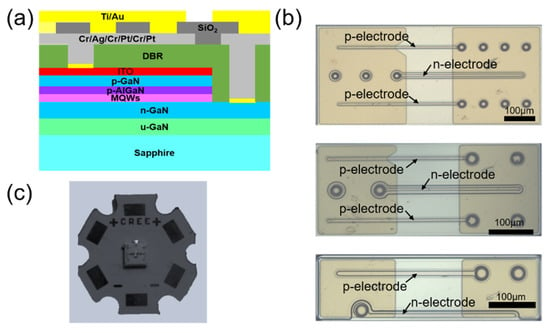
Figure 1.
(a) Schematic diagram depicting the device structure for mini-strip light-emitting diodes (LEDs). (b) Optical photos of mini-strip LEDs (scale bar: 100 µm). (c) Flip-chipped mini-strip LEDs mounted on the ceramic substrate for testing.
3. Results and Discussion
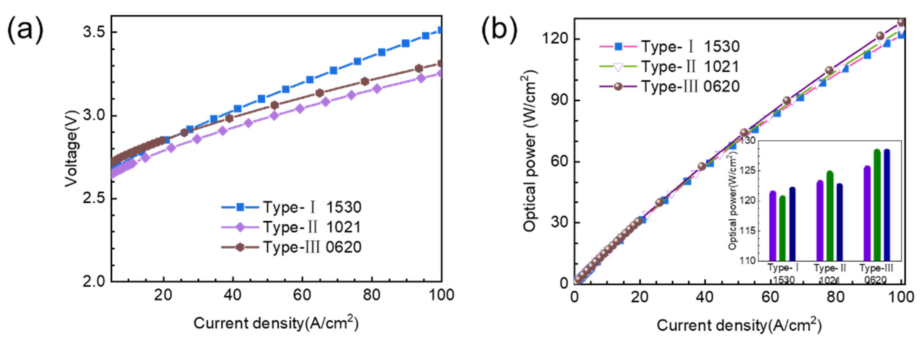
As shown in Figure 2a, no obvious size-dependent variations in the J-V characteristics can be found among these LED devices. To give a full picture, results from three randomly chosen LEDs are presented for a same size. The operating voltages of all LEDs are very similar, with a variation less than 0.1 V as the injection density increased from 0 to 30 A/cm2 and up to ~0.3 V at injection density approaching 100 A/cm2, which shows that the electrical performance of all types of LED devices are quite uniform. Moreover, the operating voltages of LEDs with the same size are almost identical as increasing the current injection densities. For a fair comparison, light output power (LOP) density was used in this study, defined as the total LOP divided by the actual light-emitting area of the devices. Figure 2b shows the LOP density of three types of LEDs versus injected current density, in which it could be found that as current injection density increased from 0 to 50 A/cm2, the LOP density exhibits no significant difference. As the current injection density goes higher, there is a noticeable increase in the LOP density for the mini-strip LEDs (Type-III). Particularly, at a current injection density of 100 A/cm2, the average LOP density for these three types of LEDs are 121.24 W/cm2 (Type-I), 124.06 W/cm2 (Type-II), and 127.33 W/cm2 (Type-III), respectively. An enhancement by 3.92 W/cm2 and 6.09 W/cm2 has been achieved as compared with the large-size LEDs (Type-II and Type-I, respectively). The inset shows the LOP densities of all LED chips with different sizes at 100 A/cm2.
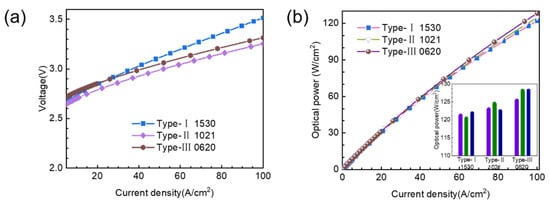
Figure 2.
(a) Size-dependent electrical characteristics as a function of current density. (b) Light output power (LOP) density for all types of LEDs versus current density. Inset shows the LOP densities at 100 A/cm2.
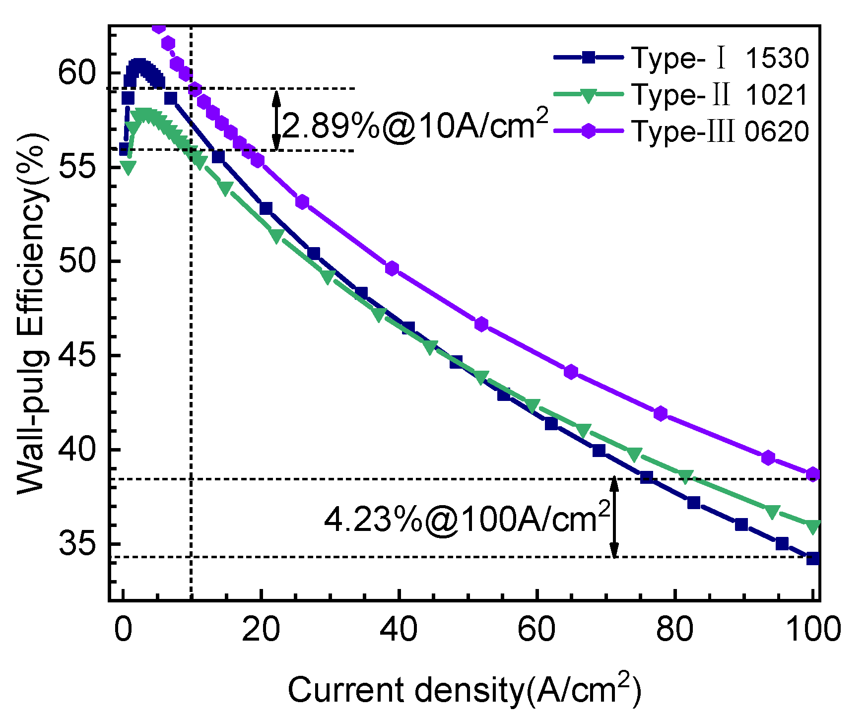
Figure 3 shows the size-dependent wall-plug efficiencies (WPE) of all three types of LEDs versus the current injection density. When the current density is less than 60 A/cm2, the WPE of Type-II LEDs on average is around 1.5% lower than that of Type-I LEDs. As the current injection density further increases to 80 A/cm2, the WPE completely exceeds that of Type-I LEDs. Meanwhile, when the current injection density is less than 10 A/cm2, the WPE of mini-strip LEDs (Type-III) is only about 1.85% and 2.89% higher than that of Type-I and Type-II LEDs, respectively, on average (Type-III: 57.88%, 57.75%, 57.14%; Type-I: 55.4%, 55.56%, 56.25%). As the current injection density increases to 100 A/cm2, the WPE increases by about 4.23% on average (Type-III: 38.7%, 38.68%, 37.67%; Type-I: 34.43%, 34.23%, 34.69%). The improvement in the WPE can be mainly attributed to two aspects: (1) better current spreading for the mini-strip LEDs, and (2) more light extracted from the LED sidewalls due to the strip-shaped geometric [40].
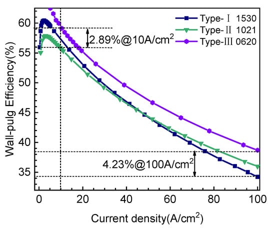
Figure 3.
Size-dependent wall-plug efficiencies for Type-I, II, and III LEDs versus current density.
With increasing the current density, the current crowding effect for the LED chips become severer, which thereafter seriously affects their luminous efficiency and reliability. According to the simple one-dimensional circuit model [41], the current spreading length (Ls) can be obtained by the following formula:
where denotes the distance from the mesa edge to the center, denotes the current density on the mesa edge, is the specific contact resistivity of metal and p-GaN, and , , , and are the resistivity and thickness of p-GaN and n-GaN, respectively. By using the parameters = 4.0 Ω cm, = 0.03 Ω cm, and = 0.005 Ω cm2 and layer thicknesses = 0.08 µm and = 2 µm, the current spreading length is calculated to be 183 µm. From the above formula, it can be known that the is only related to the resistivity and thickness of the n-GaN layer, the resistivity and thickness of the p-GaN layer, and the p-type contact resistance, as the n-type ohmic contact is usually much better. Since all LEDs were processed in the same batch, the current spreading ability is only related to the LED geometrical structure. It can be quantitatively estimated by checking the light emission intensity over the distance between the p- and n-electrodes on the mesa, which should partially reflect the current density profile. The scanning light intensity profile from the n-electrode to the mesa edge is shown in Figure 4a. The light emission intensity of Type-I LED dramatically reduces from 0.62 to 0.46 W/cm2. In contrast, it slightly reduces from 0.52 to 0.51 W/cm2 for Type-II LEDs and from 0.44 to 0.42 W/cm2 for Type-III LEDs, demonstrating the light emission uniformity can be improved by using mini-strip geometrics, which is consistent with results from similar LED strip structure yet with much larger size [40]. In addition, the overall light emission distribution for all LED devices is shown in Figure 4b. In terms of color variations, representing the light emission intensity uniformity, the improvement can be easily distinguished for Type-II and Type-III LEDs. Although current spreading is almost identical for these two kinds of LEDs, the light extraction efficiency of Type-III LEDs is higher than that of Type-II LEDs, as the metal electrodes would block the emission from the QWs. Therefore, to achieve higher quantum efficiency, the current spreading should be considered, which calls for a closer configuration of p/n metal contacts, while on the other hand, the absorption of metal contacts cannot be ruled out, for the light extraction efficiency of the LED will degrade concurrently, which limits the size of mini-strip LEDs further getting smaller.
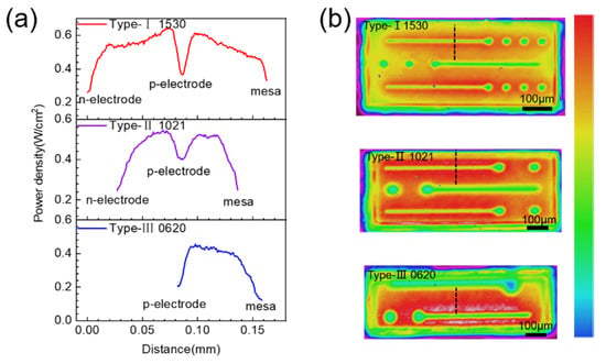
Figure 4.
(a) p to n contact (b) overall light output power intensity distribution for the Type-I, Type-II, and Type-III LEDs.
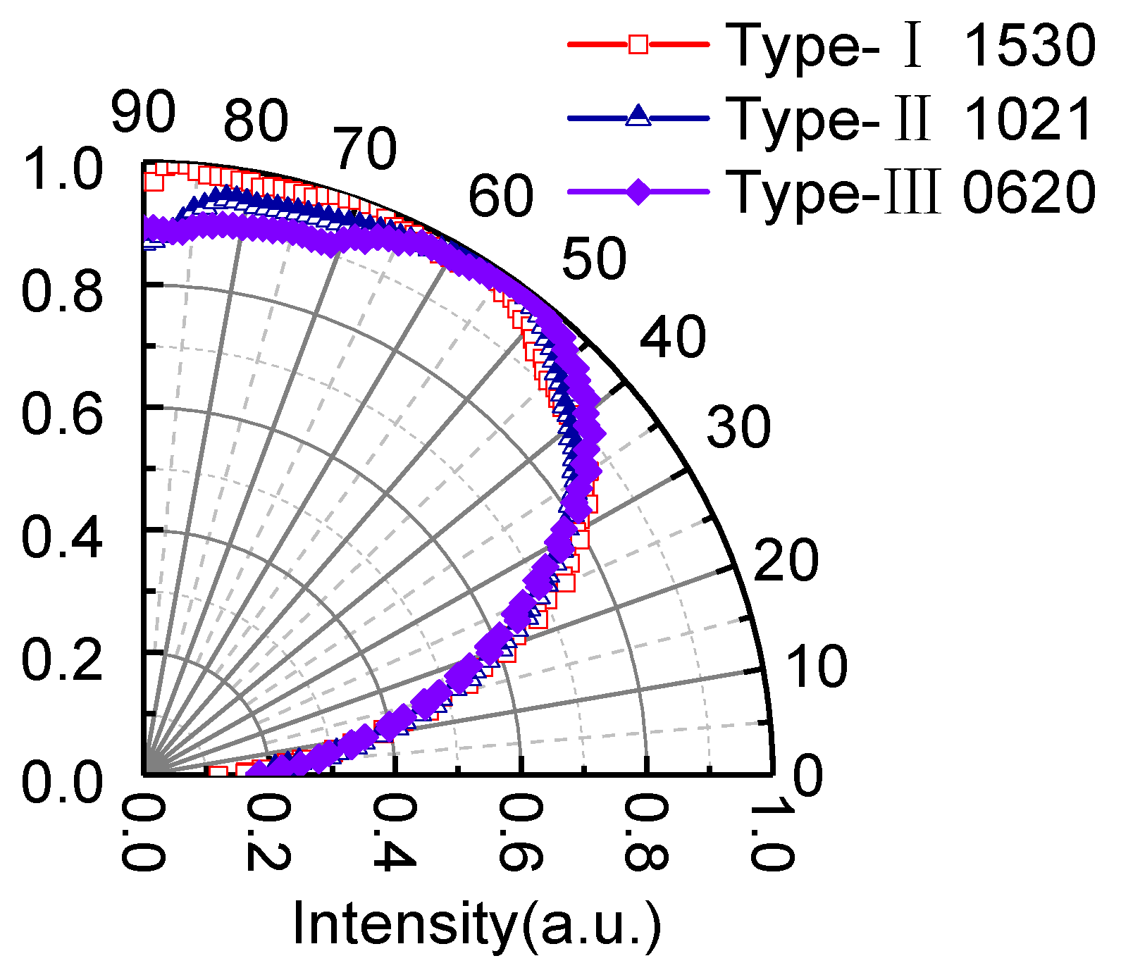
As shown in Figure 5, the impact of LED geometrics on the side emission are confirmed by the angular far-field light intensity distribution measurement, from which we can see Type-I LED chips emit the strongest light at about 60° to 90°, while Type-II LEDs exhibit the strongest intensity at 55° to 85° and mini-strip LEDs (Type-III) at about 50° to 70°. It can be clearly identified that with the gradual decrease of chip width, the edge emission becomes more dominant, affirming that the enhancement in the LOP density is also out of the increased side emission [40,42].

Figure 5.
Angular far-field light intensity distribution for the Type-I, Type-II and Type-III LEDs at a current density of 100 A/cm2.
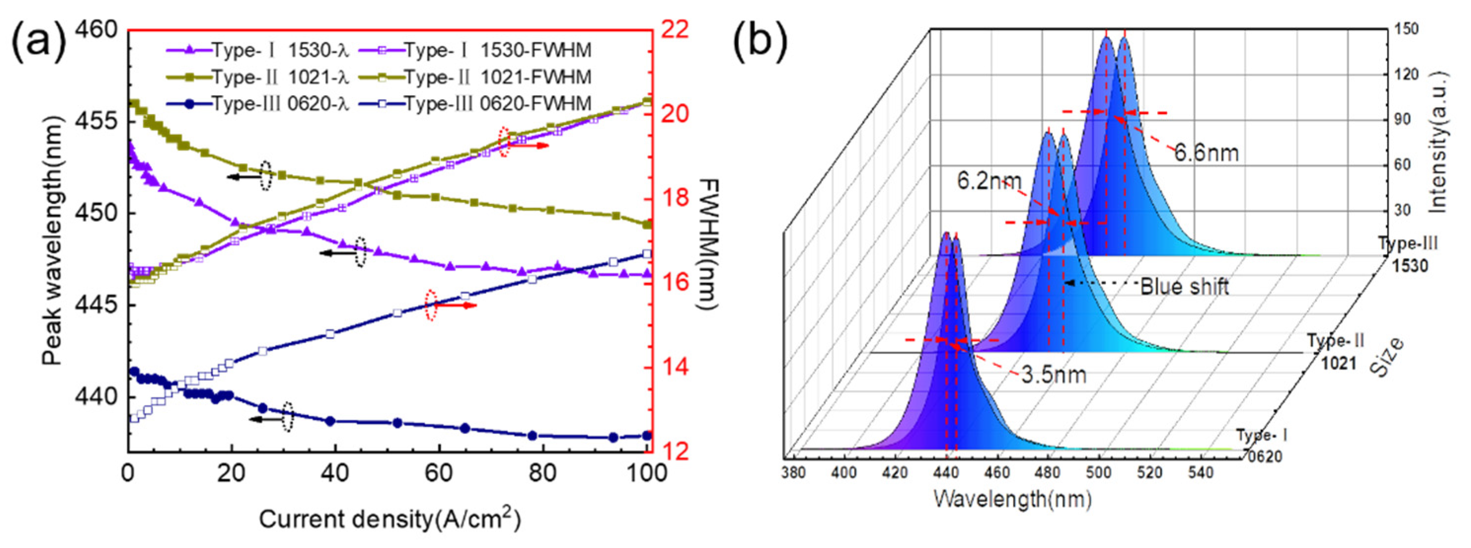
The existence of the spontaneous and built-in piezoelectric fields within InGaN MQWs leads to the quantum-confined Stark effect (QCSE), which causes the energy bands to bend, thereby reducing the overlap integral of the electron-hole wave functions [16]. In the case of high current injection density, the band-filling effect and shielding of the electrical field in the active area would reduce QCSE, which will cause a blueshift in the emission wavelength. In Figure 6a, the spectral peak wavelengths for Type-I, Type-II, and Type-III LEDs are 453.3, 455.6, and 441.4 nm at the current density of 1 A/cm2, and shift to 446.7, 449.4, and 437.9 nm at 100 A/cm2, which exhibits blueshifts by 6.6, 6.2, and 3.5 nm, respectively. The smaller blueshift with mini-strip LEDs may be attributed to a better current spreading by reducing the carrier density that alleviates the band-filling effect in MQWs. Meanwhile, the full width half maximum (FWHM) of the three types of LED are 16.3, 16.0, and 12.8 nm at the current density of 1 A/cm2, and 20.3, 20.3, and 16.7 nm at 100 A/cm2, with an increase of 4, 4.3, and 3.9 nm, respectively, as shown in Figure 6b. The smaller broadening of FWHM in mini-strip LEDs may be attributed to the alleviated band-filling effect in MQWs and less self-heating effect, leading to lower operating temperatures than the other two sizes of LEDs. The smaller wavelength blueshift and narrower FWHM indicate that light emission from the mini-strip LEDs is more stable, even under a high current injection density reaching up to 100 A/cm2 [43].

Figure 6.
(a) Size-dependent characteristics of peak wavelength and full width half maximum (FWHM) versus current density. (b) Electroluminescence spectra of LEDs with different sizes driven at 1 A/cm2 and at 100 A/cm2 current densities.
Nonradiative recombination process will cause severe self-heating problem, which would significantly degrade the device performance and its lifetime. At high current injection conditions, Auger recombination is regarded as the most critical factor contributing to the nonradiative recombination rate, which is strongly related to the carrier densities according to the ABC model. Hence, self-heating effects are mainly determined by the over-crowding injected carrier densities. Due to the flip-chip configuration, the devices suffer fewer thermal effects, with no obvious redshifts observed in the emission wavelengths even at the current density up to 100 A/cm2. It is still reflected by the variations of LED operating temperatures. As shown in Figure 7a, at low current injection density of 10 A/cm2, the operating temperatures of these three types of LED chips are very close, within a variation of 1 °C. While current injection gets higher, the operating temperatures of these three types of LED chips exhibits larger divergence, reaching a maximum gap of almost 12 °C. The increase in the LED operating temperature is consistent with the WPE results, which also shows that mini-strip chip arrays are more suitable for high output power devices than single large-area mesa LED chips. Figure 7b shows the infrared camera photos of each type of LED chip at a current injection density of 100 A/cm2. In detail, the average operating temperature of Type-III LEDs is around 37 °C, whereas the operating temperatures of Type-II and Type-I LEDs are about 4.5 °C and 11.3 °C higher, respectively. The decrease in the operating temperature will extend the lifespan of the devices.
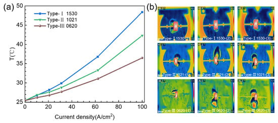
Figure 7.
(a) Size-dependent LED operating temperature versus current density. (b) Infrared images of all LEDs with different sizes operating at a current density of 100 A/cm2.
4. Conclusions
In this study, the performance of mini-strip LED chips has been demonstrated as superior to large-sized chips throughout all current injection density up to 100 A/cm2. Especially, at a current injection density of 100 A/cm2, the light output power densities are 3.92 W/cm2 and 6.09 W/cm2 higher; as a result, the quantum efficiencies have been improved by 3.6% and 4.23%, while the operating temperatures are reduced by 4.5 °C and 11.3 °C, respectively, as compared to LEDs with larger mesa dimensions. The current spreading and light emission are more uniform. Instead of moving towards large-mesa LEDs, our work suggests that an array of rectangular mini-strip LEDs would provide a choice for achieving light sources with higher quantum efficiency at ultrahigh current injection densities.
Author Contributions
Conceptualization, all authors; methodology, Y.Z.; validation, X.Z., Z.L. and Z.M.; formal analysis, X.Z.; investigation, X.Z. and Y.L.; resources, M.L.; data curation, X.Z., Y.L. and Y.Z.; writing—original draft preparation, X.Z.; writing—review and editing, Y.Z.; supervision, G.W.; project administration, X.Y.; funding acquisition, J.L. All authors have read and agreed to the published version of the manuscript.
Funding
This research was funded by National Key Research and Development Program of China (No. 2017YFB0403100, 2017YFB0403103), National Natural Science Foundation of China (No. 61974140, 61604140), and Chinese Academy of Sciences.
Data Availability Statement
The data presented in this study are available upon reasonable request from the corresponding author.
Acknowledgments
The authors wish to thank the anonymous reviewers for their valuable suggestions.
Conflicts of Interest
The authors declare no conflict of interest.
References
- Wierer, J.J.; David, A.; Megens, M.M. III-nitride photonic-crystal light-emitting diodes with high extraction efficiency. Nat. Photonics 2009, 3, 163–169. [Google Scholar] [CrossRef]
- Wu, H.; Li, H.; Kuo, S.Y.; Chen, B.Y.; Lu, T.C.; Huang, H. High Output Power GaN-Based Green Resonant-Cavity Light-Emitting Diodes With Trapezoidal Quantum Wells. IEEE Trans. Electron Devices 2020, 67, 3650–3654. [Google Scholar] [CrossRef]
- Zhang, Y.; Xie, H.; Zheng, H.; Wei, T.; Yang, H.; Li, J.; Yi, X.; Song, X.; Wang, G.; Li, J. Light extraction efficiency improvement by multiple laser stealth dicing in InGaN-based blue light-emitting diodes. Opt. Express 2012, 20, 6808. [Google Scholar] [CrossRef]
- Day, J.; Li, J.; Lie, D.Y.C.; Bradford, C.; Lin, J.Y.; Jiang, H.X. III-Nitride full-scale high-resolution microdisplays. Appl. Phys. Lett. 2011, 99, 42. [Google Scholar] [CrossRef]
- Wu, T.; Chin-Wei, S.; Yue, L.; Chun-Fu, L.; Liang, S.; Lu, Y.; Huang, S.W.; Guo, W.; Hao-Chung, K.; Zhong, C. Mini-LED and Micro-LED: Promising Candidates for the Next Generation Display Technology. Appl. Sci. 2018, 8, 1557. [Google Scholar] [CrossRef]
- Olivier, F.; Tirano, S.; Dupré, L.; Aventurier, B.; Largeron, C.; Templier, F. Influence of size-reduction on the performances of GaN-based micro-LEDs for display application. J. Lumin. 2016, 191, 112–116. [Google Scholar] [CrossRef]
- Wang, Z.; Shan, X.; Cui, X.; Tian, P. Characteristics and techniques of GaN-based micro-LEDs for application in next-generation display. J. Semicon. 2020, 41, 81–86. [Google Scholar] [CrossRef]
- McKendry, J.J.D.; Green, R.P.; Kelly, A.E.; Gong, Z.; Guilhabert, B.; Massoubre, D.; Gu, E.; Dawson, M.D. High-Speed Visible Light Communications Using Individual Pixels in a Micro Light-Emitting Diode Array. IEEE Photonics Technol. Lett. 2010, 22, 1346–1348. [Google Scholar] [CrossRef]
- Konthoujam, J.S.; Huang, Y.M.; Ahmed, T.; Singh, K.J. Micro-LED as a Promising Candidate for High-Speed Visible Light Communication. Appl. Sci. 2020, 10, 7384. [Google Scholar]
- Huang, Y.; Guo, Z.; Wang, X.; Li, H.; Xiang, D. GaN-based high response frequency and high optical power matrix micro-LED for visible light communication. IEEE Electron Device Lett. 2020, 41, 1536–1539. [Google Scholar] [CrossRef]
- Narukawa, Y.; Ichikawa, M.; Sanga, D.; Sano, M.; Mukai, T. White light emitting diodes with super-high luminous efficacy. J. Phys. D Appl. Phys. 2010, 43, 354002. [Google Scholar] [CrossRef]
- Li, P.P.; Zhao, Y.B.; Li, H.J.; Che, J.M.; Wang, G.H. Very high external quantum efficiency and wall-plug efficiency 527 nm InGaN green LEDs by MOCVD. Opt. Express 2018, 26, 33108. [Google Scholar] [CrossRef] [PubMed]
- Polkovnikov, A.S.; Zegrya, G.G. Auger Recombination in Semiconductor Quantum Wells. Phys. Rev. B 1998, 58, 247–250. [Google Scholar] [CrossRef]
- Delaney, K.T.; Rinke, P.; Walle, C.G.V.D. Auger recombination rates in nitrides from first principles. Appl. Phys. Lett 2009, 94, 141101. [Google Scholar] [CrossRef]
- Kioupakis, E.; Yan, Q.; van de Walle, C.G. Interplay of polarization fields and Auger recombination in the efficiency droop of nitride light-emitting diodes. Appl. Phys. Lett. 2012, 101, 180. [Google Scholar] [CrossRef]
- David, A.; Grundmann, M.J. Influence of polarization fields on carrier lifetime and recombination rates in InGaN-based light-emitting diodes. Appl. Phys. Lett. 2010, 97, 033501. [Google Scholar] [CrossRef]
- Ryu, H.Y.; Shin, D.S.; Shim, J.-L. Analysis of efficiency droop in nitride light-emitting diodes by the reduced effective volume of InGaN active material. Appl. Phys. Lett. 2012, 100, 2217. [Google Scholar] [CrossRef]
- Malyutenko, V.K.; Bolgov, S.S.; Podoltsev, A.D. Current crowding effect on the ideality factor and efficiency droop in blue lateral InGaN/GaN light emitting diodes. Appl. Phys. Lett. 2010, 97, 180. [Google Scholar] [CrossRef]
- Narukawa, Y.; Kawakami, Y.; Fujita, S.; Fujita, S.; Nakamura, S. Recombination dynamics of localized excitons in In 0.20 Ga 0.80 N- In 0.05 Ga 0.95 N multiple quantum wells. Phys. Rev. B 1997, 55. [Google Scholar] [CrossRef]
- Li, H.; Li, P.; Kang, J.; Zhi, L.; Zhang, Y.; Meng, L.; Li, Z.; Jing, L.; Yi, X.; Wang, G. Analysis Model for Efficiency Droop of InGaN Light-Emitting Diodes Based on Reduced Effective Volume of Active Region by Carrier Localization. Appl. Phys. Express 2013, 6, 092101. [Google Scholar] [CrossRef]
- Hangleiter, A.; Hitzel, F.; Netzel, C.; Fuhrmann, D.; Rossow, U.; Ade, G.; Hinze, P. Suppression of nonradiative recombination by V-shaped pits in GaInN/GaN quantum wells produces a large increase in the light emission efficiency. Phys. Rev. Lett. 2005, 95, 127402. [Google Scholar] [CrossRef] [PubMed]
- Xie, J.; Ni, X.; Qian, F.; Shimada, R.; OEzguer, U.; Morkoc, H. On the efficiency droop in InGaN multiple quantum well blue light emitting diodes and its reduction with p-doped quantum well barriers. Appl. Phys. Lett. 2008, 93, 121107. [Google Scholar] [CrossRef]
- Ni, X.; Li, X.; Lee, J.; Liu, S.; Avrutin, V.; Oezguer, U.; Morkoc, H.; Matulionis, A.; Paskova, T.; Mulholland, G. InGaN staircase electron injector for reduction of electron overflow in InGaN light emitting diodes. Appl. Phys. Lett. 2010, 97, 160. [Google Scholar] [CrossRef]
- RoMer, F.; Witzigmann, B. Effect of Auger recombination and leakage on the droop in InGaN/GaN quantum well LEDs. Opt. Express 2014, 22 (Suppl. 6), A1440. [Google Scholar] [CrossRef]
- Li, C.-K.; Wu, Y.-R. Study on the Current Spreading Effect and Light Extraction Enhancement of Vertical GaN/InGaN LEDs. IEEE Trans. Electron Devices 2012, 59, 400–407. [Google Scholar] [CrossRef]
- Madhusoodhanan, S.; Sabbar, A.; Atcitty, S.; Kaplar, R.; Chen, Z. High-Temperature Analysis of GaN-based Blue LEDs for Future Power Electronic Applications. IEEE J. Emerg. Sel. Top. Power Electron. 2020, 8, 4186–4190. [Google Scholar] [CrossRef]
- Xu, J.; Schubert, M.F.; Noemaun, A.N.; Zhu, D.; Kim, J.K.; Schubert, E.F.; Min, H.K.; Chung, H.J.; Yoon, S.; Sone, C. Reduction in efficiency droop, forward voltage, ideality factor, and wavelength shift in polarization-matched GaInN/GaInN multi-quantum-well light-emitting diodes. Appl. Phys. Lett. 2009, 94, 183507. [Google Scholar] [CrossRef]
- Kuo, Y.-K.; Wang, T.-H.; Chang, J.-Y. Advantages of blue InGaN light-emitting diodes with InGaN-AlGaN-InGaN barriers. Appl. Phys. Lett. 2012, 100, 31112. [Google Scholar] [CrossRef]
- Lu, T. Advantages of GaN based light-emitting diodes with a p-InGaN hole reservoir layer. Appl. Phys. Lett. 2012, 100, 183507. [Google Scholar] [CrossRef]
- Wu, F.L.; Ou, S.L.; Kao, Y.C.; Chen, C.L.; Tseng, M.C.; Lu, F.C.; Lin, M.T.; Horng, R.H. Thin-film vertical-type AlGaInP LEDs fabricated by epitaxial lift-off process via the patterned design of Cu substrate. Opt. Express 2015, 23, 18156–18165. [Google Scholar] [CrossRef]
- Liu, W.J.; Hu, X.L.; Zhang, J.Y.; Weng, G.E.; Lv, X.Q.; Huang, H.J.; Chen, M.; Cai, X.M.; Ying, L.Y.; Zhang, B.P. Low-temperature bonding technique for fabrication of high-power GaN-based blue vertical light-emitting diodes. Opt. Mater. 2012, 34, 1327–1329. [Google Scholar] [CrossRef]
- Wang, L.; Guo, E.; Liu, Z.; Yi, X.; Wang, G. High-performance nitride vertical light-emitting diodes based on Cu electroplating technical route. IEEE Trans. Electron Devices 2016, 63, 892–902. [Google Scholar] [CrossRef]
- Kivisaari, P.; Kim, I.; Suihkonen, S.; Oksanen, J. Elimination of Lateral Resistance and Current Crowding in Large-Area LEDs by Composition Grading and Diffusion-Driven Charge Transport. Adv. Electron. Mater. 2017, 3. [Google Scholar] [CrossRef]
- Li, Y.; Wu, Q.; Meng, F.Y.; Sung, H.K.; Yao, Z.; Sun, R.Y.; Wang, C. Enhanced performance of large-area vertical light-emitting diodes treated by laser irradiation. J. Nanosci. Nanotechnol. 2017, 12, 369–372. [Google Scholar] [CrossRef]
- Zhang, Y.; Zheng, H.; Guo, E.; Cheng, Y.; Ma, J.; Wang, L.; Liu, Z.; Yi, X.; Wang, G.; Li, J. Effects of light extraction efficiency to the efficiency droop of InGaN-based light-emitting diodes. J. Appl. Phys. 2013, 113, 1274. [Google Scholar] [CrossRef]
- Wang, L.; Zhang, Z.-H.; Wang, N. Current crowding phenomenon: Theoretical and direct correlation with the efficiency droop of light emitting diodes by a modified ABC model. IEEE J. Quantum Electron. 2015, 51, 3200109. [Google Scholar]
- Lin, J.Y.; Jiang, H.X. Development of microLED. Appl. Phys. Lett. 2020, 116, 100502. [Google Scholar] [CrossRef]
- Li, C.C.; Zhan, J.L.; Chen, Z.Z.; Jiao, F.; Shen, B. Operating behavior of micro-LEDs on a GaN substrate at ultrahigh injection current densities. Opt. Express 2019, 27, A1146. [Google Scholar] [CrossRef]
- Tian, P.; Mckendry, J.J.D.; Gong, Z.; Guilhabert, B.; Watson, I.M.; Gu, E.; Chen, Z.; Zhang, G.; Dawson, M.D. Size-dependent efficiency and efficiency droop of blue InGaN micro-light emitting diodes. Appl. Phys. Lett. 2012, 101, 2217. [Google Scholar] [CrossRef]
- Cheung, W.S.; Cheung, Y.F.; Chen, H.T.; Hui, R.S.Y.; Waffenschmidt, E.; Choi, H.W. InGaN light-emitting diode stripes with reduced luminous exitance. Opt. Express 2015, 23, 15021–15028. [Google Scholar] [CrossRef]
- Guo, X.; Schubert, E.F. Current crowding and optical saturation effects in GaInN/GaN light-emitting diodes grown on insulating substrates. Appl. Phys. Lett. 2001, 78, 3337–3339. [Google Scholar] [CrossRef]
- Park, Y.; Li, K.H.; Fu, W.Y.; Cheung, Y.F.; Choi, H.W. Packaging of InGaN stripe-shaped light-emitting diodes. Appl. Opt. 2018, 57, 2452–2458. [Google Scholar] [CrossRef] [PubMed]
- Gong, Z.; Jin, S.; Chen, Y.; Mckendry, J.; Massoubre, D.; Watson, I.M.; Gu, E.; Dawson, M.D. Size-dependent light output, spectral shift, and self-heating of 400 nm InGaN light-emitting diodes. J. Appl. Phys. 2010, 107, 1086. [Google Scholar] [CrossRef]
Publisher’s Note: MDPI stays neutral with regard to jurisdictional claims in published maps and institutional affiliations. |
© 2021 by the authors. Licensee MDPI, Basel, Switzerland. This article is an open access article distributed under the terms and conditions of the Creative Commons Attribution (CC BY) license (http://creativecommons.org/licenses/by/4.0/).

