Numerical Investigation and Design of Electrically-Pumped Self-Pulsing Fano Laser Based on III-V/Silicon Integration


Abstract
:1. Introduction
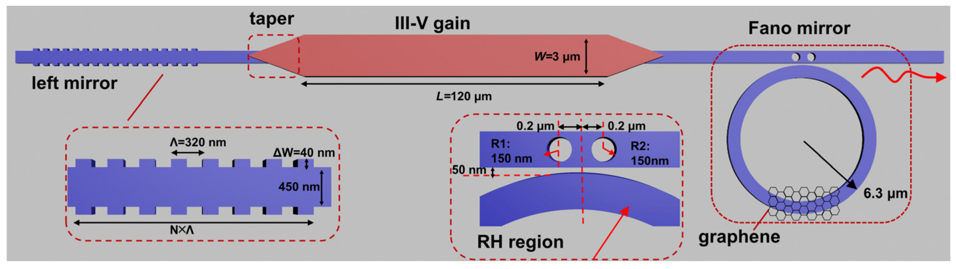
2. Device Structure and Design Optimization
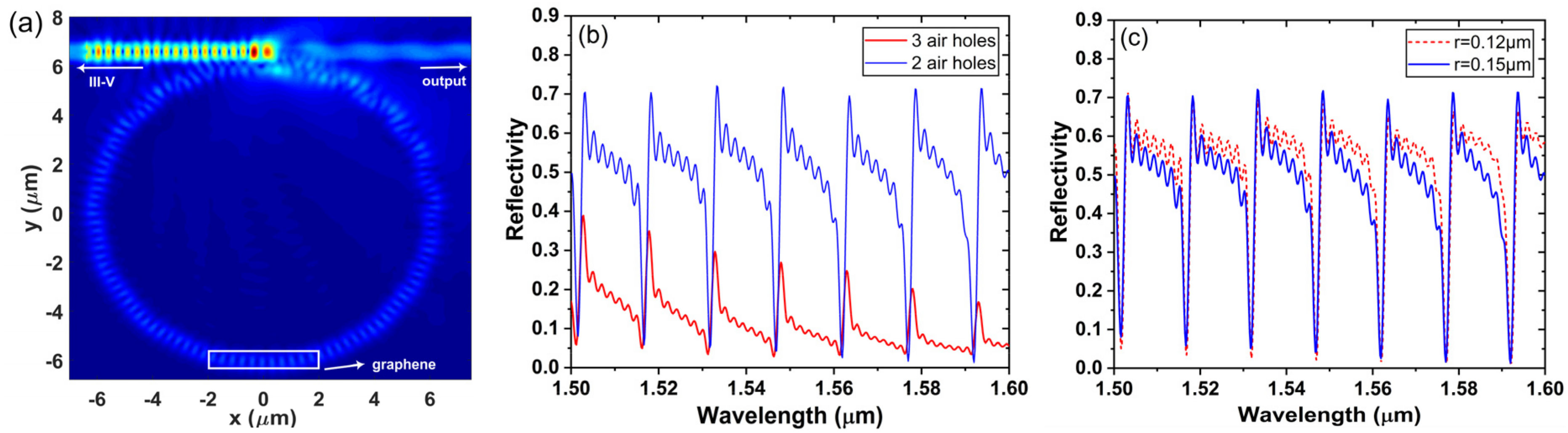
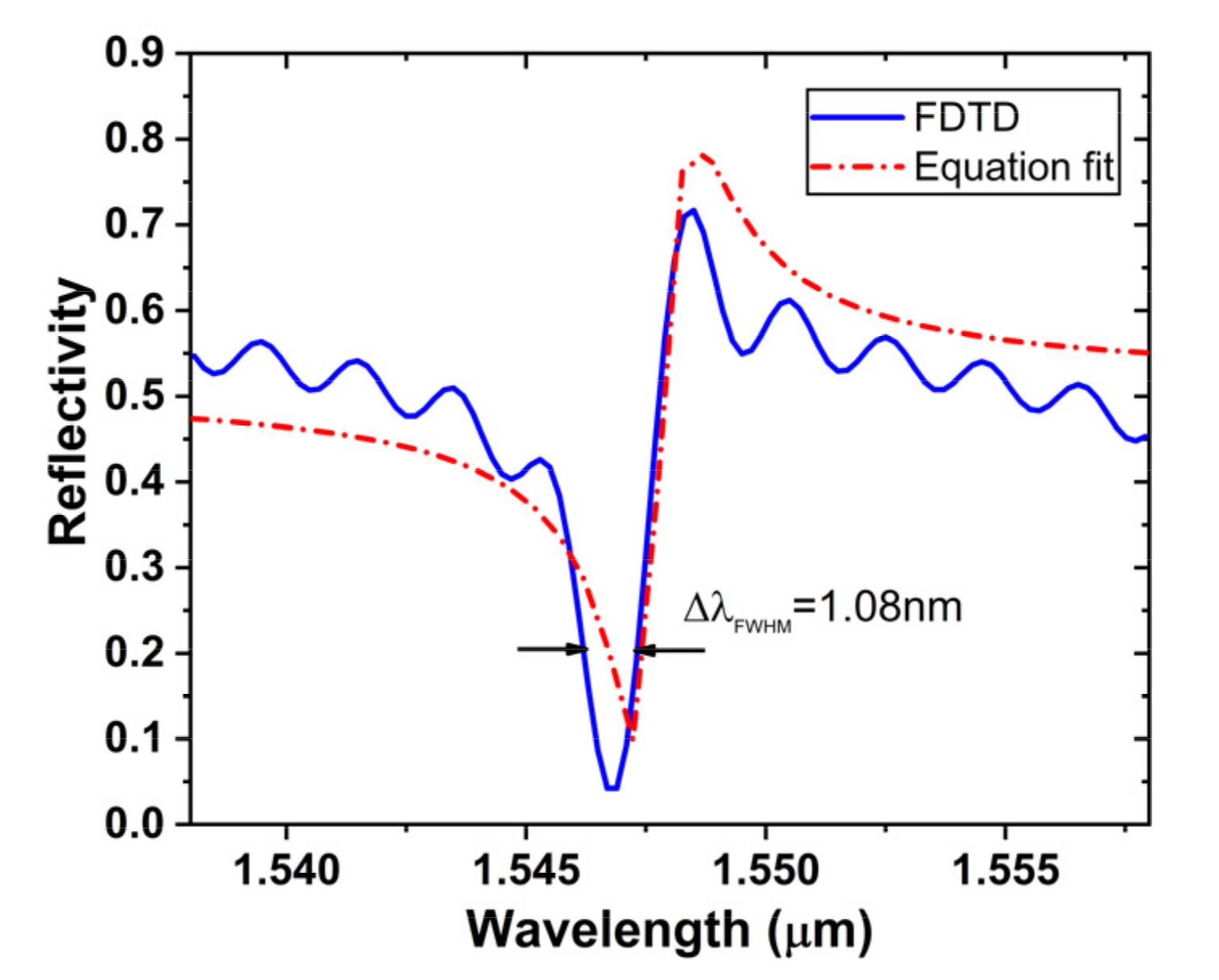
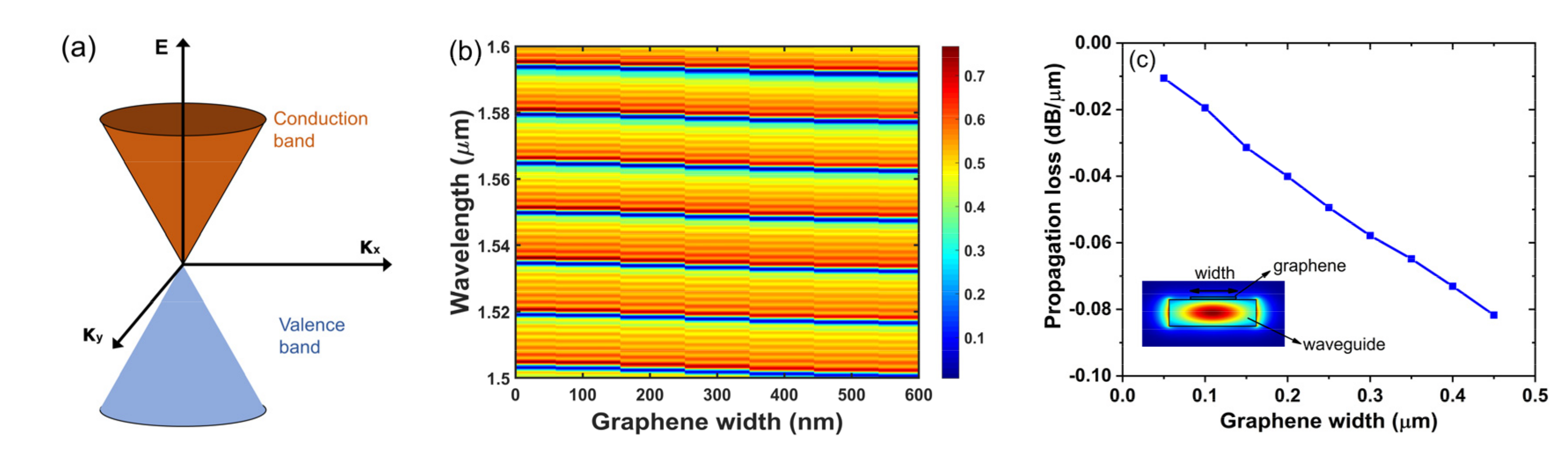
2.1. Fano Mirror
2.2. Bragg Mirrorr
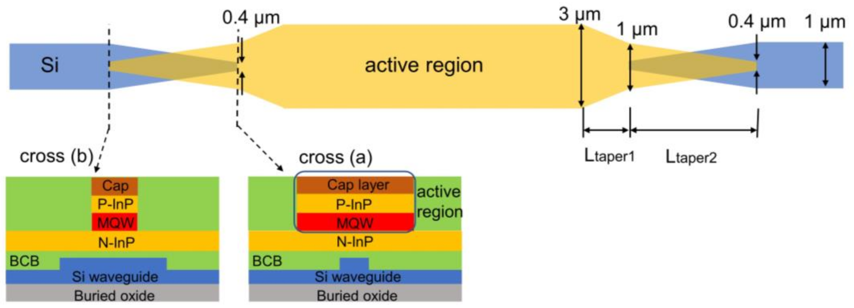
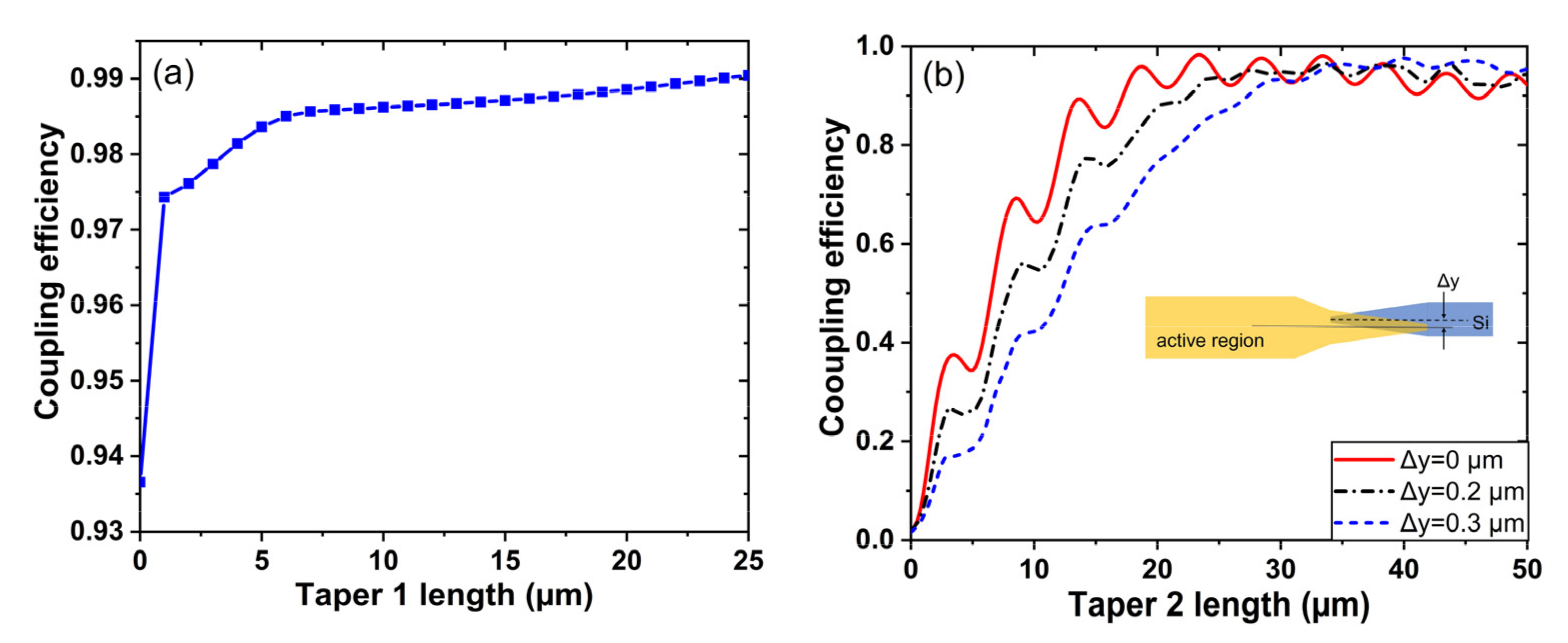
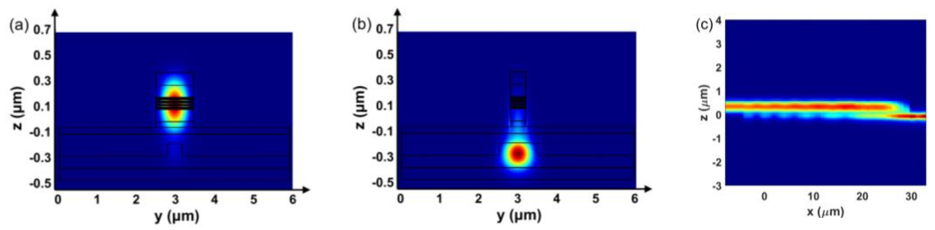
2.3. Taper Region
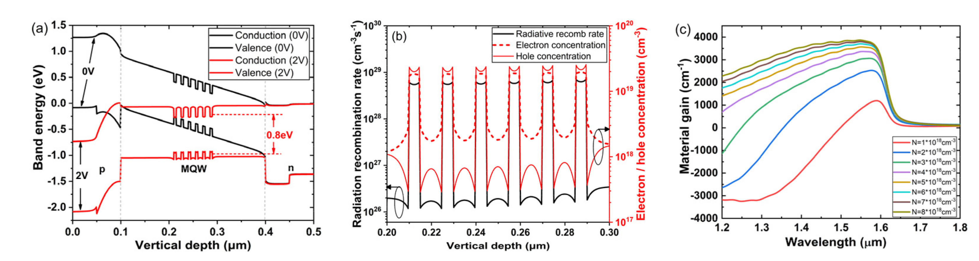
2.4. MQW Design
3. Laser Dynamics
3.1. Numerical Model
3.2. Device Performance
4. Conclusions
Author Contributions
Funding
Data Availability Statement
Acknowledgments
Conflicts of Interest
References
- Trocha, P.; Karpov, M.; Ganin, D.; Pfeiffer, M.H.P.; Kordts, A.; Wolf, S.; Krockenberger, J.; Marin-Palomo, P.; Weimann, C.; Randel, S.; et al. Ultrafast optical ranging using microresonator soliton frequency combs. Science 2018, 359, 887–891. [Google Scholar] [CrossRef] [Green Version]
- Knigge, A.; Klehr, A.; Wenzel, H.; Zeghuzi, A.; Fricke, J.; Maaßdorf, A.; Liero, A.; Tränkle, G. Wavelength-Stabilized High-Pulse-Power Laser Diodes for Automotive LiDAR. Phys. Status Solidi A 2018, 215, 1700439. [Google Scholar] [CrossRef]
- Shastri, B.J.; Tait, A.N.; Ferreira de Lima, T.; Pernice, W.H.P.; Bhaskaran, H.; Wright, C.D.; Prucnal, P.R. Photonics for artificial intelligence and neuromorphic computing. Nat. Photonics 2021, 15, 102–114. [Google Scholar] [CrossRef]
- Ghelfi, P.; Laghezza, F.; Scotti, F.; Serafino, G.; Capria, A.; Pinna, S.; Onori, D.; Porzi, C.; Scaffardi, M.; Malacarne, A.; et al. A fully photonics-based coherent radar system. Nature 2014, 507, 341–345. [Google Scholar] [CrossRef]
- Kippenberg, T.J.; Holzwarth, R.; Diddams, S.A. Microresonator-Based Optical Frequency Combs. Science 2011, 332, 555–559. [Google Scholar] [CrossRef]
- Hou, L.; Haji, M.; Marsh, J.H.; Bryce, A.C. 490 fs pulse generation from a passive C-band AlGaInAs/InP quantum well mode-locked laser. Opt. Lett. 2012, 37, 773–775. [Google Scholar] [CrossRef] [PubMed]
- Thiessen, T.; Poon, J.K.S. 20 GHz Mode-Locked Laser Diodes with Integrated Optical Feedback Cavities in a Generic Monolithic InP Photonics Platform. IEEE Photonics J. 2017, 9, 1505010. [Google Scholar] [CrossRef]
- Nielsen, L.; Bente, E.A.J.M.; den Haan, E.; Heck, M.J.R. Theoretical and Experimental Investigation of Unidirectionality in an Integrated Semiconductor Ring Mode-Locked Laser with Two Saturable Absorbers. IEEE J. Quantum Electron. 2018, 54, 2000810. [Google Scholar] [CrossRef] [Green Version]
- Keyvaninia, S.; Uvin, S.; Tassaert, M.; Fu, X.; Latkowski, S.; Marien, J.; Thomassen, L.; Lelarge, F.; Duan, G.; Verheyen, P.; et al. Narrow-linewidth short-pulse III–V-on-silicon mode-locked lasers based on a linear and ring cavity geometry. Opt. Express 2015, 23, 3221–3229. [Google Scholar] [CrossRef] [Green Version]
- Davenport, M.L.; Liu, S.; Bowers, J.E. Integrated heterogeneous silicon/III–V mode-locked lasers. Photonics Res. 2018, 6, 468–478. [Google Scholar] [CrossRef]
- Huang, D.; Tran, M.A.; Guo, J.; Peters, J.; Komljenovic, T.; Malik, A.; Morton, P.A.; Bowers, J.E. High-power sub-kHz linewidth lasers fully integrated on silicon. Optica 2019, 6, 745–752. [Google Scholar] [CrossRef] [Green Version]
- Wang, R.; Haq, B.; Sprengel, S.; Malik, A.; Vasiliev, A.; Boehm, G.; Simonyte, I.; Vizbaras, A.; Vizbaras, K.; Van Campenhout, J.; et al. Widely tunable III–V/silicon lasers for spectroscopy in the short-wave infrared. IEEE J. Sel. Top. Quantum Electron. 2019, 25, 1502412. [Google Scholar] [CrossRef]
- Tang, M.; Park, J.-S.; Wang, Z.; Chen, S.; Jurczak, P.; Seeds, A.; Liu, H. Integration of III–V lasers on Si for Si photonics. Prog. Quantum Electron. 2019, 66, 1–18. [Google Scholar] [CrossRef]
- Keyvaninia, S.; Uvin, S.; Tassaert, M.; Wang, Z.; Fu, X.; Latkowski, S.; Marien, J.; Thomassen, L.; Lelarge, F.; Duan, G.; et al. III–V-on-silicon anti-colliding pulse-type mode-locked laser. Opt. Lett. 2015, 40, 3057–3060. [Google Scholar] [CrossRef] [PubMed] [Green Version]
- Srinivasan, S.; Norberg, E.; Komljenovic, T.; Davenport, M.; Fish, G.; Bowers, J.E. Hybrid Silicon Colliding-Pulse Mode-Locked Lasers With On-Chip Stabilization. IEEE J. Sel. Top. Quantum Electron. 2015, 21, 24–29. [Google Scholar] [CrossRef]
- Cuyvers, S.; Haq, B.; Op de Beeck, C.; Poelman, S.; Hermans, A.; Wang, Z.; Gocalinska, A.; Pelucchi, E.; Corbett, B.; Roelkens, G.; et al. Low Noise Heterogeneous III–V-on-Silicon-Nitride Mode-Locked Comb Laser. Laser Photonics Rev. 2021, 15, 2000485. [Google Scholar] [CrossRef]
- Luo, H.; Li, J.; Zhu, C.; Liu, Y. Dual-waveband self-pulsed laser at 3 μm and 2.1 μm. IEEE Photonics Technol. Lett. 2019, 31, 1033–1036. [Google Scholar] [CrossRef]
- Akahane, K.; Matsumoto, A.; Umezawa, T.; Yamamoto, N. High-frequency short-pulse generation with a highly stacked in as quantum dot mode-locked laser diode. Jpn. J. Appl. Phys. 2021, 60, SBBH02. [Google Scholar] [CrossRef]
- Afkhamiardakani, H.; Diels, J.-C. Controlling group and phase velocities in bidirectional mode-locked fiber lasers. Opt. Lett. 2019, 44, 2903–2906. [Google Scholar] [CrossRef]
- Zaugg, C.A.; Sun, Z.; Wittwer, V.J.; Popa, D.; Milana, S.; Kulmala, T.S.; Sundaram, R.S.; Mangold, M.; Sieber, O.D.; Golling, M.; et al. Ultrafast and widely tuneable vertical-external-cavity surface-emitting laser, mode-locked by a graphene-integrated distributed Bragg reflector. Opt. Express 2013, 21, 31548–31559. [Google Scholar] [CrossRef] [PubMed] [Green Version]
- Sun, Z.; Martinez, A.; Wang, F. Optical modulators with 2D layered materials. Nat. Photonics 2016, 10, 227–238. [Google Scholar] [CrossRef] [Green Version]
- Yamashita, S. Nonlinear optics in carbon nanotube, graphene, and related 2D materials. APL Photonics 2019, 4, 034301. [Google Scholar] [CrossRef] [Green Version]
- FDTD Solution and Mode Solution. Available online: https://www.lumerical.com/ (accessed on 10 July 2021).
- Gu, L.; Fang, L.; Fang, H.; Li, J.; Zheng, J.; Zhao, J.; Zhao, Q.; Gan, X. Fano resonance lineshapes in a waveguide-microring structure enabled by an air-hole. APL Photonics 2020, 5, 016108. [Google Scholar] [CrossRef] [Green Version]
- Xu, Y.; Li, Y.; Lee, R.K.; Yariv, A. Scattering-theory analysis of waveguide-resonator coupling. Phys. Rev. E 2000, 62, 7389–7404. [Google Scholar] [CrossRef]
- Fan, S. Sharp asymmetric line shapes in side-coupled waveguide-cavity systems. Appl. Phys. Lett. 2002, 80, 908–910. [Google Scholar] [CrossRef] [Green Version]
- Rasmussen, T.S.; Yu, Y.; Mork, J. Suppression of coherence collapse in semiconductor Fano lasers. Phys. Rev. Lett. 2019, 123, 233904. [Google Scholar] [CrossRef] [Green Version]
- Davenport, M.L.; Heck, M.J.R.; Bowers, J.E. Characterization of a Hybrid Silicon-InP Laser Tapered Mode Converter. In Proceedings of the 2013 Conference on Lasers and Electro-Optics Europe (CLEO EUROPE), Munich, Germany, 12–16 May 2013. [Google Scholar]
- SILVACO. Semiconductor Process and Device Simulation. Atlas Package. Available online: https://silvaco.com/tcad/ (accessed on 20 August 2021).
- Yanping, X.; Wei-Ping, H.; Xun, L. An efficient solution to the standing-wave approach based on cold cavity modes for simulation of DFB lasers. J. Lightwave Technol. 2009, 27, 3227–3234. [Google Scholar] [CrossRef]
- Tromborg, B.; Olesen, H.; Pan, X.; Saito, S. Transmission line description of optical feedback and injection locking for Fabry-Perot and DFB lasers. IEEE J. Quantum Electron. 1987, 23, 1875–1889. [Google Scholar] [CrossRef]
- Yu, Y.; Xue, W.; Semenova, E.; Yvind, K.; Mork, J. Demonstration of a self-pulsing photonic crystal Fano laser. Nat. Photonics 2017, 11, 81–84. [Google Scholar] [CrossRef] [Green Version]
- Ohtsubo, J. Semiconductor Lasers Stability, Instability and Chaos, 2nd ed.; Springer: Berlin/Heidelberg, Germany, 2008. [Google Scholar]


| Layer | Material | Thickness (nm) | Refractive Index |
|---|---|---|---|
| P-spacer | InP | 55 | 3.21 |
| P-blocking layer | In0.53Al0.47As | 45 | 3.23 |
| Top GRINSCH | In0.51Al0.39Ga0.1As | 100 | 3.25 |
| 7 × Barriers | In0.54Al0.32Ga0.14As | 8 | 3.38 |
| 6 × Wells | In0.7Al0.152Ga0.148As | 5 | 3.39 |
| Bottom GRINSCH | In0.51Al0.39Ga0.1As | 100 | 3.25 |
| N-blocking layer | In0.53Al0.47As | 45 | 3.23 |
| N-spacer | InP | 55 | 3.21 |
| Bonding layer | DVS-BCB | 80 (on top of ridge) | 1.57 |
| 180 (outside ridge region) | |||
| Waveguide layer | Si | 220 | 3.476 |
| Parameters | Symbol (Unit) | Value |
|---|---|---|
| Effective index of the active region | 3.2 | |
| Group refractive index of the active region | 3.5 | |
| Linewidth enhancement factor | 3.5 | |
| Transparency carrier density | (cm−3) | 1017 |
| Confinement factor | 0.047 | |
| Material gain coefficient | (cm−1) | 3800 |
| Length of the active layer | (μm) | 120 |
| Active layer width | (μm) | 3 |
| Carrier lifetime | (ns) | 0.4 |
| Photon lifetime | (ps) | 0.8 |
| Bimolecular radiation coefficient | (10−10 cm3 s−1) | 1 |
| Auger coefficient | (10−29 cm6 s−1) | 3 |
| Reflection coefficient of RH | 0.76 | |
| Quality factor of the microring | 1429 | |
| Decay rate of the microring | (Hz) | 6.8 × 10¹⁰ |
| Coupling rate from microring to the waveguide | (Hz) | 4.7 × 10¹⁰ |
Publisher’s Note: MDPI stays neutral with regard to jurisdictional claims in published maps and institutional affiliations. |
© 2021 by the authors. Licensee MDPI, Basel, Switzerland. This article is an open access article distributed under the terms and conditions of the Creative Commons Attribution (CC BY) license (https://creativecommons.org/licenses/by/4.0/).
Share and Cite
Zhao, Y.; Li, Y.; Huang, W. Numerical Investigation and Design of Electrically-Pumped Self-Pulsing Fano Laser Based on III-V/Silicon Integration. Photonics 2021, 8, 530. https://doi.org/10.3390/photonics8120530
Zhao Y, Li Y, Huang W. Numerical Investigation and Design of Electrically-Pumped Self-Pulsing Fano Laser Based on III-V/Silicon Integration. Photonics. 2021; 8(12):530. https://doi.org/10.3390/photonics8120530
Chicago/Turabian StyleZhao, Yingming, Yu Li, and Weiping Huang. 2021. "Numerical Investigation and Design of Electrically-Pumped Self-Pulsing Fano Laser Based on III-V/Silicon Integration" Photonics 8, no. 12: 530. https://doi.org/10.3390/photonics8120530
APA StyleZhao, Y., Li, Y., & Huang, W. (2021). Numerical Investigation and Design of Electrically-Pumped Self-Pulsing Fano Laser Based on III-V/Silicon Integration. Photonics, 8(12), 530. https://doi.org/10.3390/photonics8120530