Abstract
A 1.55 μm AlGaInAs multi-quantum-well (MQW) ridge waveguide polarization mode controller (PMC) is proposed. The design is based on an asymmetric half-ridge waveguide structure in which the ridge is shallow etched on one side and has a deeply etched mesa structure on the other side. The Finite-Element Method (FEM) was used to simulate the PMC and optimize its structural parameters comprehensively. Furthermore, the fabrication tolerances were also investigated in detail. The optimized PMC has a polarization conversion efficiency (PCE) of around 92.5% with a half-beat length of 1250 μm. When the PMC length was fixed at 1250 μm, to achieve a PCE derivation less than 8%, the tolerances for the ridge waveguide width and shallow etch height were 1.60 μm to 1.65 μm and 2.13 μm to 2.18 μm, respectively. In order to reduce interband gap absorption loss, the quantum well intermixing (QWI) technique was used in the model to realize a blueshift (200 nm) in the PMC. QWI is a simple, flexible, and low-cost technique for fabricating a PMC integrated with a laser diode and reduces parasitic reflections, which would otherwise degrade the overall performance. QWI also eliminates MQW material anisotropy and alleviates the birefringence effect without the need for regrowth, achieving nearly uniform properties as a bulk material.
1. Introduction
Controlling and manipulating the polarization of light has extensive applications including ‘coherent-lite’ optical communications [1], polarimetry, and quantum key distribution [2]. Polarization mode controllers (PMCs), which are often incorporated in waveguides on photonic integrated circuits (PICs), can convert transverse electric (TE) to transverse magnetic (TM) modes and vice versa. Good mode-matching between the waveguides of monolithic PMCs and laser diodes (LDs) is critical for their integration. Given the growing number of LDs using a multi-quantum well (MQW) structure to enhance their efficiency, PMCs based on the MQW structure are desirable. Many PMCs have been reported based on different material systems, such as InGaAsP/InP [3], AlGaAs/GaAs [4], and AlGaAsSb/InGaSb [5]. However, most of these PMC devices are based on bulk material rather than MQW structures. In order to integrate bulk material PMCs with LDs based on MQW structures, researchers have to use relatively complicated butt-joint PIC techniques involving regrowth. Although an InGaAsP MQW PMC using a particular design (a 400 nm thick 1.25 Q layer underneath the MQW structure) has been reported [6], its maximum polarization conversion efficiency (PCE) was not stated. Compared with bulk-material PMCs, the inherent birefringence of MQW PMCs needs to be taken into account [6], which disturbs the optimal rotation of state of polarization (SOP) on the Poincaré sphere, and this is the most challenging aspect of an MQW-based PMC design.
Certain types of asymmetric waveguides have been reported to reduce the footprint and wavelength dependency of PMCs, including slanted sidewall waveguides [7] and angled-facet waveguide structures [8]. However, there are no reports of a systematic analysis of MQW-based PMCs, and most of the aforementioned structures are unsuitable for integrating PMCs with LDs, because the fabrication procedures for the PMC sections are not compatible with those for the LD section. Recently, PMCs based on the reactive ion-etching (RIE) lag effect [4] and half-ridge structures [3] have been proposed to improve compatibility for monolithic integration. The RIE lag-based structure contains single or multiple shallow etched slots placed asymmetrically across the width of a ridge waveguide, but the TE–TM conversion efficiency is sensitive to the slot position, width, and depth, all of which are very difficult to fabricate with sufficient precision. In particular, the depths of the slots are dependent on the RIE lag effect, affected by many parameters in the RIE system. On the other hand, a half-ridge structure decreases the fabrication tolerances by combining a shallow etched ridge structure on one side with a deeply etched mesa structure on the other. A PCE of more than 95% and a large etching time tolerance of ±16% has been reported using this design for a bulk-material-based PMC [3].
In this paper, a 1.55 μm AlGaInAs MQW PMC based on a conventional LD structure is proposed for converting the polarization state of light from the TE mode to the TM mode; it is shown that a high PCE can be obtained. In order to reduce direct interband absorption in the PMC, quantum-well intermixing (QWI) technology was used to blueshift the bandgap absorption edge by 200 nm in the PMC section [9]. QWI is a technique for the selective postgrowth tuning of the quantum well band edge across a wafer using a relatively simple procedure. The QWI used in PMC has the following advantages: (1) it alleviates the waveguide birefringence effects associated with MQWs in the PMC because, in the limit of complete intermixing, the MQW structure essentially becomes a bulk layer, and its material anisotropy disappears [10]; (2) it reduces parasitic reflections between LD and PMC that would otherwise degrade their performance; (3) it widens the bandgap and so reduces the waveguide absorption loss [11]; (4) The regrowth can be eliminated completely when the PMC is monolithically integrated with a sidewall grating DFB laser. Therefore, QWI is a simple, flexible, and low-cost technique for integrating a PMC with a LD. The waveguide losses (α) of a shallow etched ridge waveguide, 2.5 µm-wide, with its bandgap blue-shifted by 100 nm, have been measured by the Fabry-Pérot fringe method [12] and were found to be 4.1 cm−1 for the TE mode and 2.0 cm−1 for the TM mode at the operating wavelength of 1.55 μm [13]. The PMC waveguide uses a half-ridge structure design. The Finite-Element Method (FEM) was used to simulate the waveguide structure comprehensively in order to maximize the PCE and evaluate the fabrication tolerances. The PCE depends on the width of the ridge waveguide and the ridge depths on each side. By taking advantage of the 20-fold etching selectivity between AlInGaAs and InGaAsP/InP using CH4/H2-based RIE, we could precisely control etching within the waveguide core. We analyzed the mode profiles in the waveguide as well as the geometrical fabrication tolerances. As a result, a PCE of around 92% was obtained in an AlGaInAs MQW-based waveguide with a length of around 1250 μm.
2. Design and Optimization
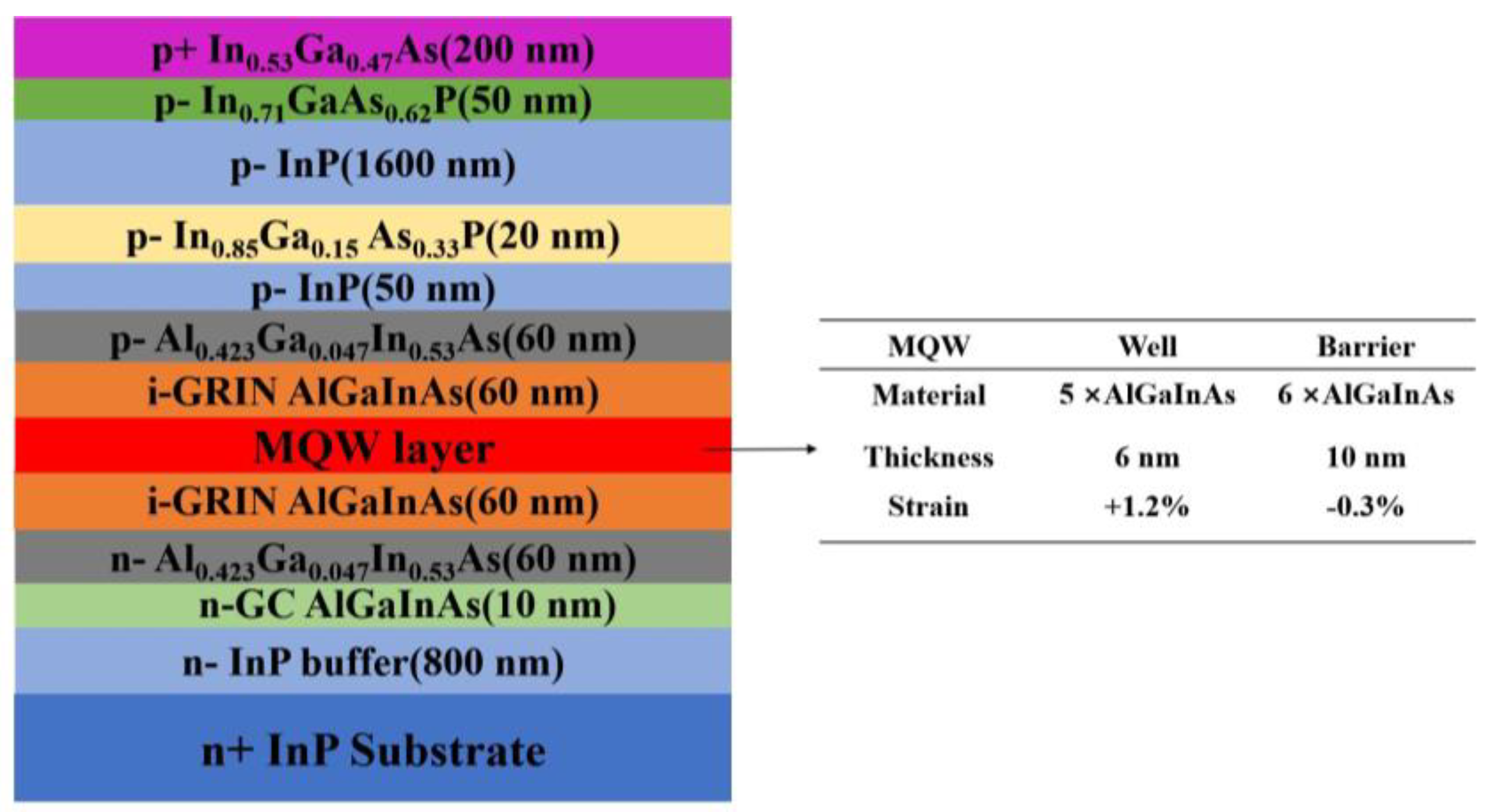
The epitaxial layer profile of the PMC was that of a conventional 1.55 µm AlGaInAs/InP LD [14] grown on a sulfur-doped InP substrate via metal–organic vapor phase epitaxy (MOVPE) in a single step. The epitaxial structure is shown in Figure 1. It comprises an 800 nm-thick n-InP buffer, a 10 nm n-type graded-composition AlGaInAs layer, a 60 nm-thick n-AlGaInAs cladding layer, and a 60 nm-thick bottom graded-index separate confinement heterostructure (GRINSCH) AlGaInAs layer with an Al composition varying from 0.423 to 0.338. The MQW structure comprises five 6 nm-thick compressively strained (+1.2%) AlGaInAs Wells and six 10 nm-thick tensile strained (−0.3%) AlGaInAs barriers. Above the active layers, there is a 60 nm-thick top GRINSCH layer and a 60 nm-thick p-AlGaInAs cladding layer, 50 nm of p-InP, a 20 nm-thick In0.85Ga0.15As0.33P0.67 quaternary wet etch stop layer with a bandgap wavelength of 1.1 μm (1.1Q), a 1600 nm-thick p-InP cladding layer, a 50 nm-thick p-In0.71GaAs0.62P (1.3Q) layer, and a 200 nm-thick p+ InGaAs contact layer. The compressive strain in the AlGaInAs QWs results in TE-polarized laser operation because of the quantum mechanical selection rules.
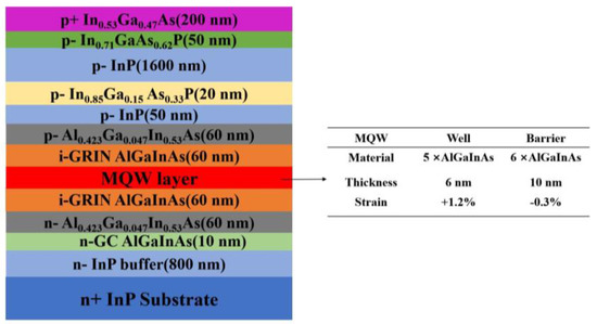
Figure 1.
The epitaxial layer structure of the PMC.
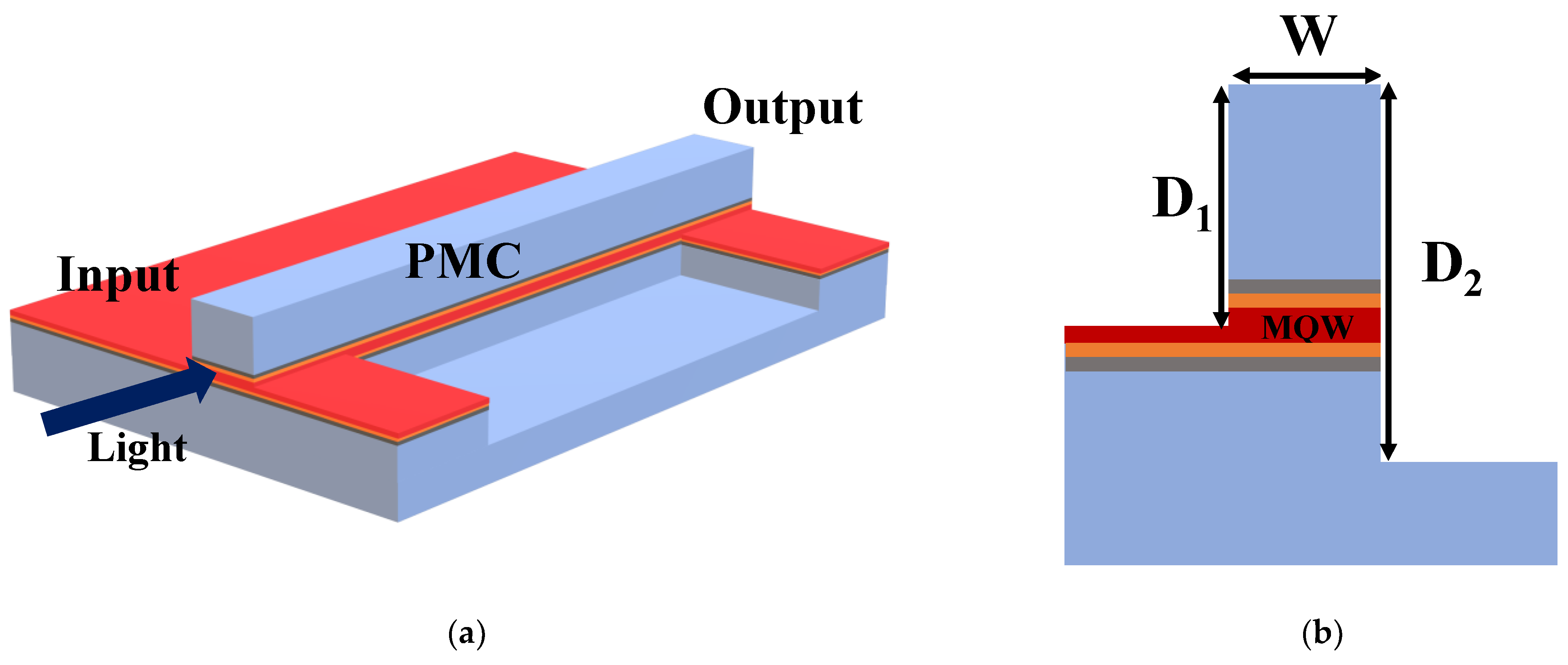
Here, we studied the efficiency of converting the TE mode to the TM mode. A schematic of the PMC is depicted in Figure 2. It consists of an input section, a PMC section in the middle, and an output section. The input and output sections are symmetric ridge waveguides etched to the same depth as the shallow etched side of the PMC. A ridge waveguide etched to different depths on each side forms the half-ridge-based PMC. When light with TE polarization is launched into the asymmetric waveguide, two fundamental eigenmodes are excited, which transforms the input light into the TM mode after propagating the half-beat length Lπ, which is given by:
where β1 and β2 are the propagation constants of the two fundamental modes, i.e., the TE0 and TM0 modes. After propagating a distance Lπ, the two eigenmodes in the PMC are rotated by 45° with respect to the modes in the input waveguide, generating a pure TM-polarized output. Hence, to shorten the PMC, the difference between β1 and β2 should be large. This design required optimizing the ridge waveguide’s shallow etched depth (D1) and width (W). It is noted that when D was sufficiently large (>3.55 µm), it had almost no effect on the eigenmode profiles. From the obtained eigenmodes, the PCE was calculated as in [15]:
where is the tilt angle of the principal axis of the eigenmodes, given approximately as with Ex and Ey being the x- and y-components of the electric field, respectively, and L is the length of the PMC. To optimize the PMC structure automatically, the EME Solver (Eigenmode Expansion Solver, one of the tools in the Lumerical software package) was employed in combination with a self-written script that links to the FEM calculation results. Appropriate ranges were set for the waveguide width (W) and shallow etched depths (D1), and the program randomly chose a set of values within these ranges to define the dimensions of a waveguide structure. The EME solver then calculated the PCE, which is dependent on these dimensions. The optimum structure with a maximum PCE can be found by scanning a wide range of W (divided into a grid of 50 elements) and D1 (divided into a grid of 20 elements).

Figure 2.
(a) Schematic of half-ridge PMC with an AlGaInAs MQW layer, (b) cross section of the PMC.
3. Simulation and Results
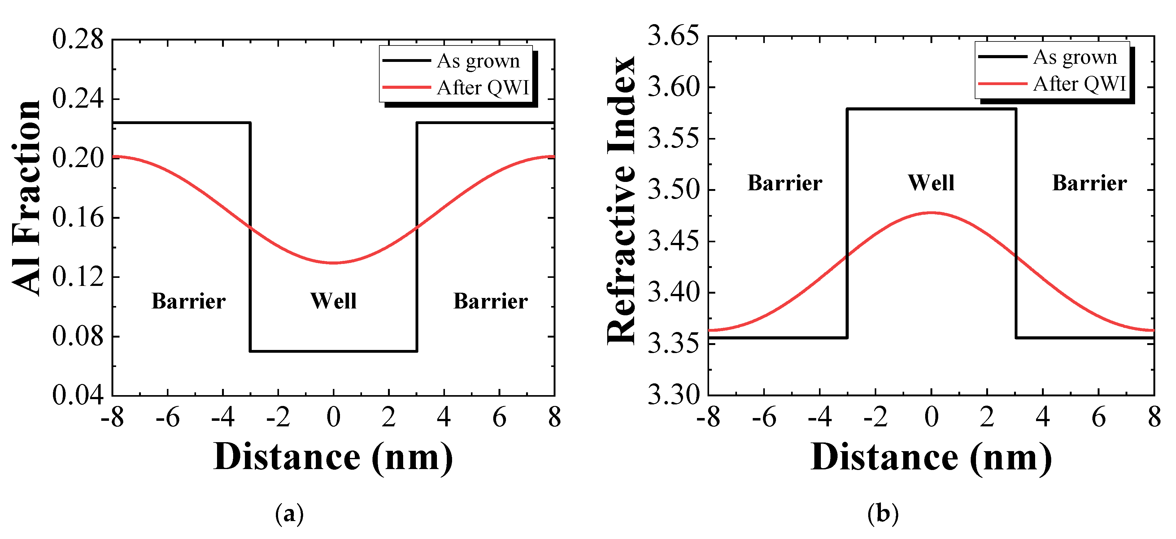
Figure 3 presents the Al composition and refractive index distribution at a wavelength of 1.55 μm in the quantum well and barrier after 200 nm blue shift with Al atom diffusion length of 2.45 nm. The as-grown reflective indexes of quantum well and barrier were 3.579 and 3.356, respectively. Following QWI, the index curve showed smooth rather than stepped variations at the interfaces between the intermixed wells and the barriers, and the effective average index of the core layer was 3.4168. The birefringence effects associated with the MQW were largely removed, and the waveguide core had similar characteristics to those of a bulk layer. The key parameters of the MQW before and after QWI are shown in Table 1. Figure 4 shows the effective refractive index (Neff) of four-mode profiles (TE0, TM0, TE1, TM1) as a function of W. From Figure 4, a range of W can be identified in which only the two fundamental modes (TE0 and TM0) can propagate in the PMC. This range of W is between 1.45 μm and 3.10 μm.
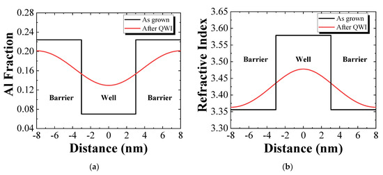
Figure 3.
(a) Al composition and (b) reflective index distribution at 1.5 µm wavelength through one period of the MQW after intermixing by 200 nm.

Table 1.
Key parameters of the as-grown MQW structure and after bandgap widening by 200 nm using QWI.
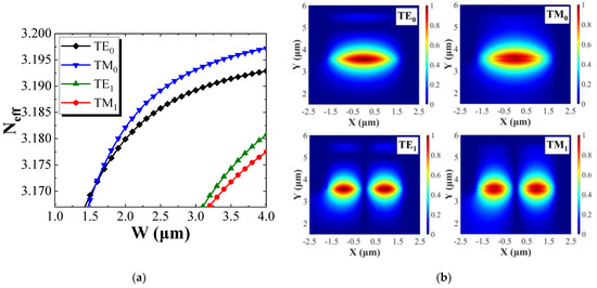
Figure 4.
(a) Simulated waveguide effective refractive index of TE0, TM0, TE1, TM1 modes as a function of the ridge waveguide width W with D1 = 2.16 μm and D2 = 3.64 μm. (b) Electric field profiles of TE0 and TM0, TE1 and TM1 modes (W = 3.50 μm).
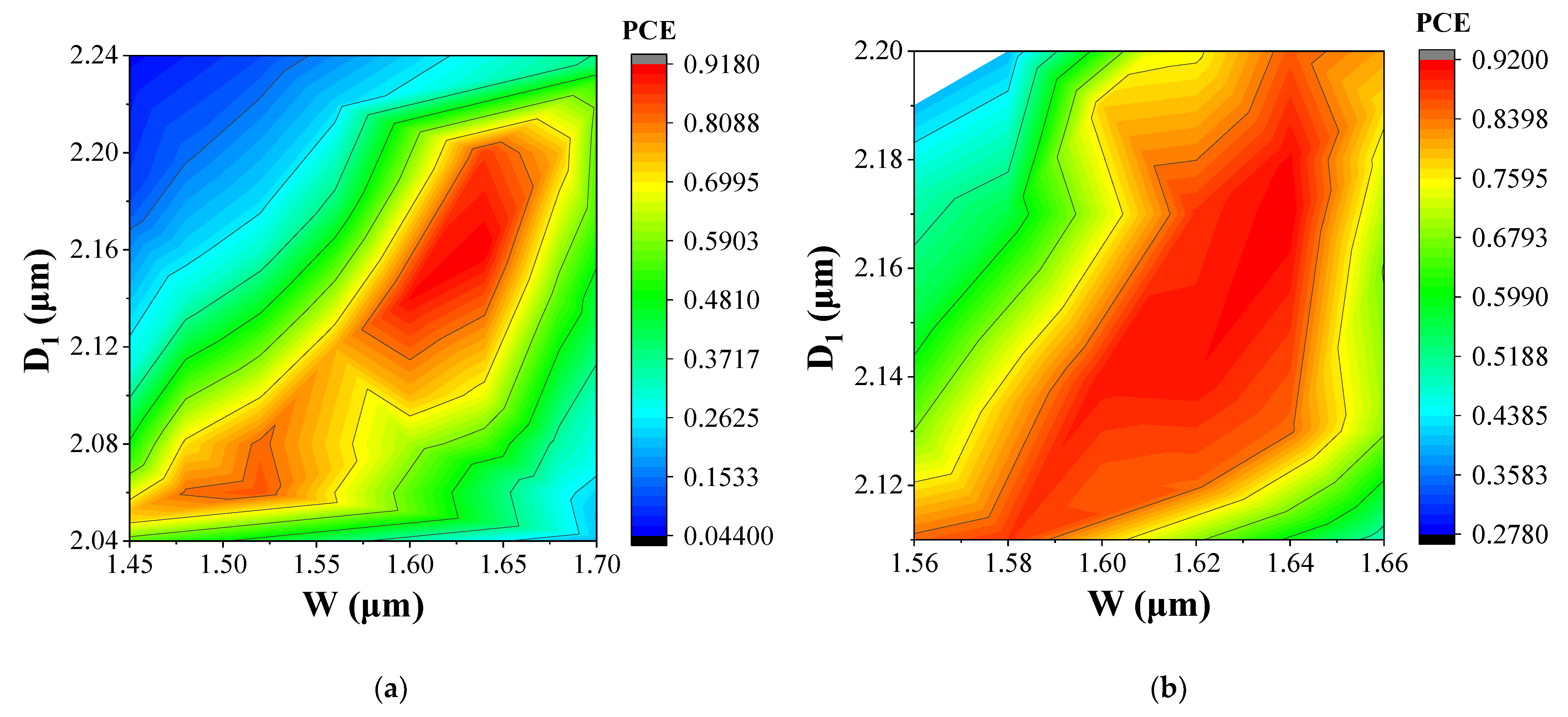
Following this stage, optimization using the EME solver was undertaken over the broad range of waveguide widths (W) from 1.45 μm to 1.70 μm and shallow etched depths (D1) from 2.04 μm to 2.24 μm. In this optimization step, the program obtained 1000 simulation data points by dividing the initial range of W into 50 grids and that of D1 into 20 grids. Then, 200 data points were randomly selected to calculate their maximum PCE. The input source was assumed to be 100% TE-polarized light. Figure 5a shows a 2D plot of the variation of the maximum PCE as a function of W and D1. The ‘MAX PCE’ required the PMC length (L) to be the corresponding half-beat length (Lπ).

Figure 5.
Maximum TE–TM PCE as a function of waveguide width (W) and shallow etched depth (D1) from (a) broad-range optimization and (b) narrow-range optimization.
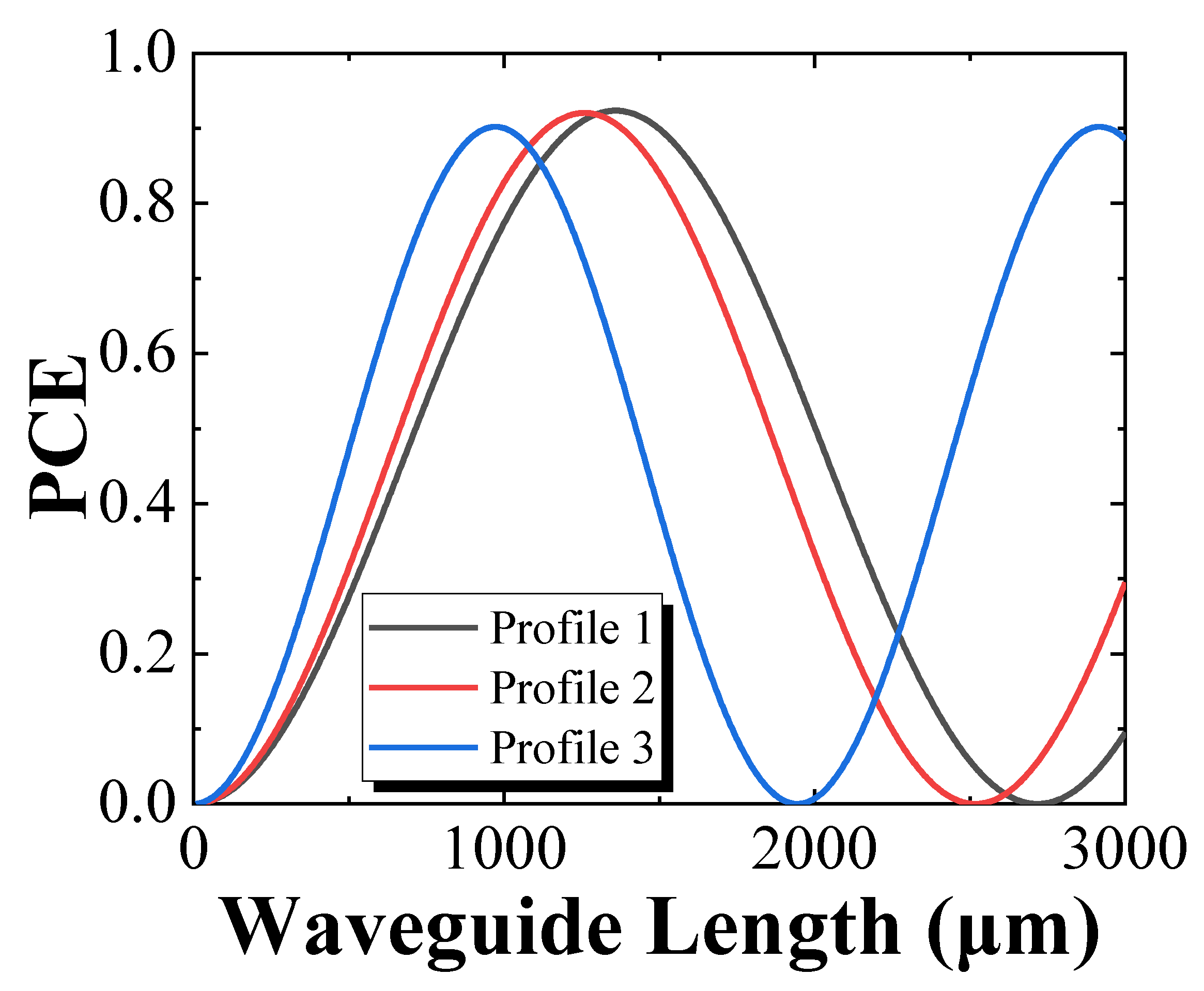
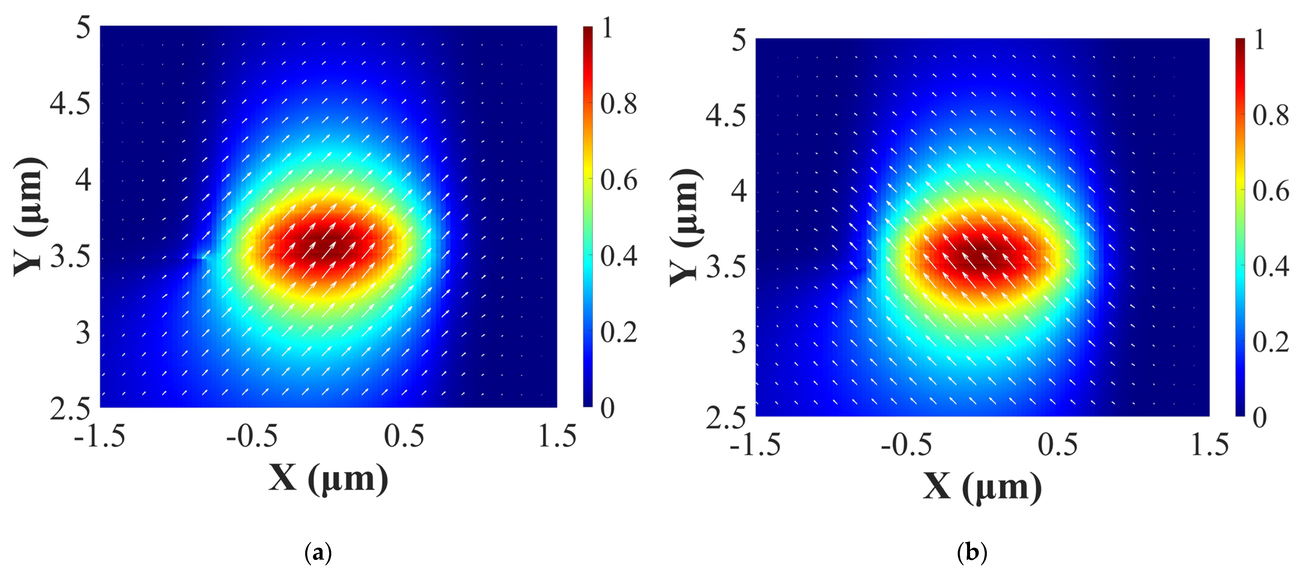
Data points with a PCE larger than 70% clustered around specific value ranges, namely, D1 from 2.10 μm to 2.20 μm, and W from 1.56 μm to 1.66 μm. Further simulations, focused on a narrower span of these variables, were therefore carried out, and the results are shown in Figure 5b. Based on these calculations, three PMC profiles with a high PCE and relatively short half-beat length (Lπ) were identified. The periodic PCE curves and waveguide parameters of these three profiles are shown in Figure 6 and Table 2, respectively. A maximum TE–TM PCE of 94% was obtained for profile 3. As a waveguide with a longer Lπ would exhibit increased absorption and make the device footprint larger, profile 2 represents a good balance between PCE and Lπ. Figure 7 shows the electric field profiles of the first two TE0 and TM0 eigenmodes of a PMC with profile 2. The modes are confined by the AlGaInAs MQW core, and the fractions of TE and TM polarization are almost equal, confirming that the polarization of the modes in PMC are tilted by approximately 45° with respect to the mode in the input section, which is 100% TE polarized.
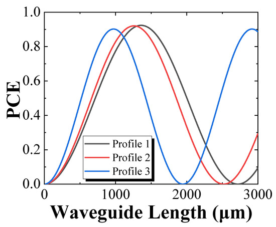
Figure 6.
Periodic PCE curves of the three profiles.

Table 2.
Three profiles of waveguide parameters.
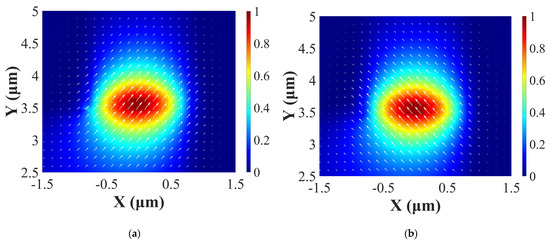
Figure 7.
Electric field profiles of (a) TE0 and (b) TM0 eigenmodes for D1 = 2.16 μm, D2 = 3.64 μm, W = 1.62 μm.
4. Tolerance Analysis
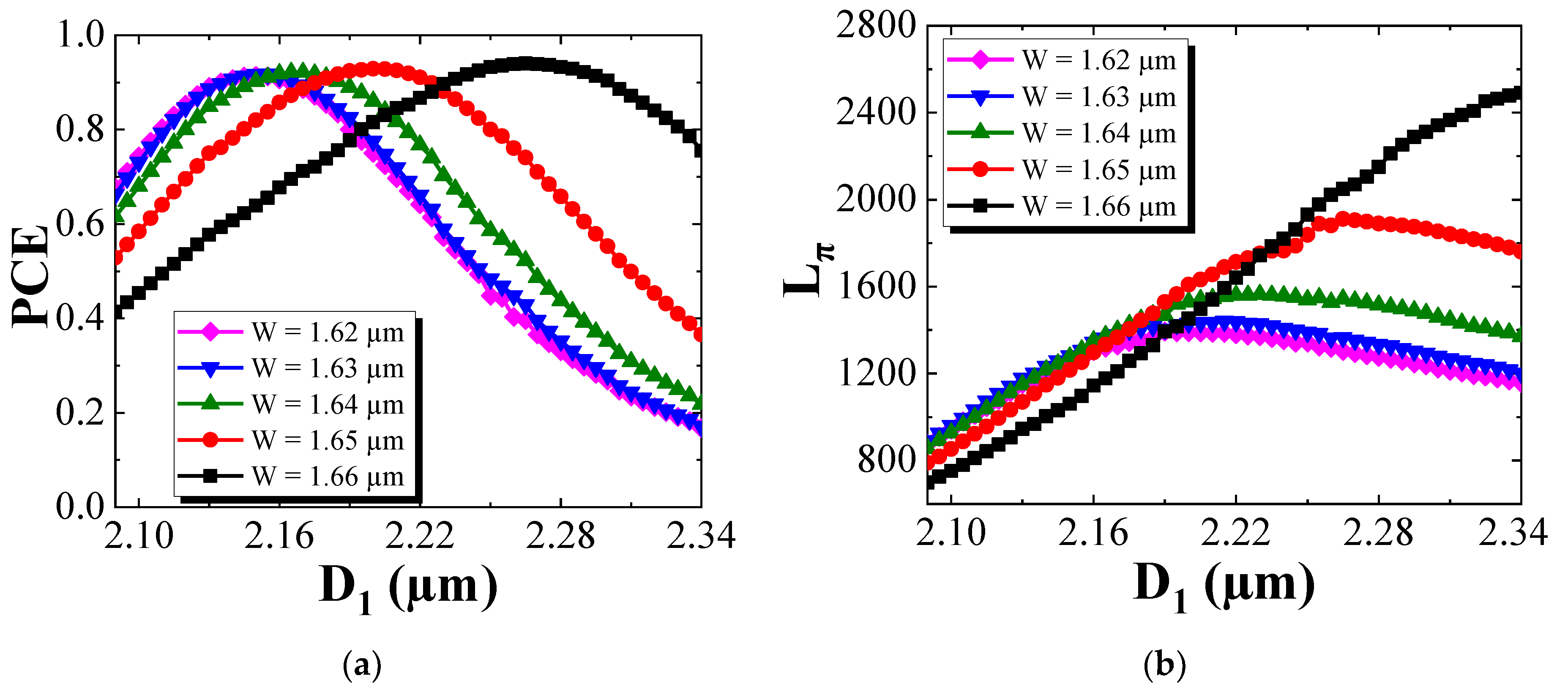
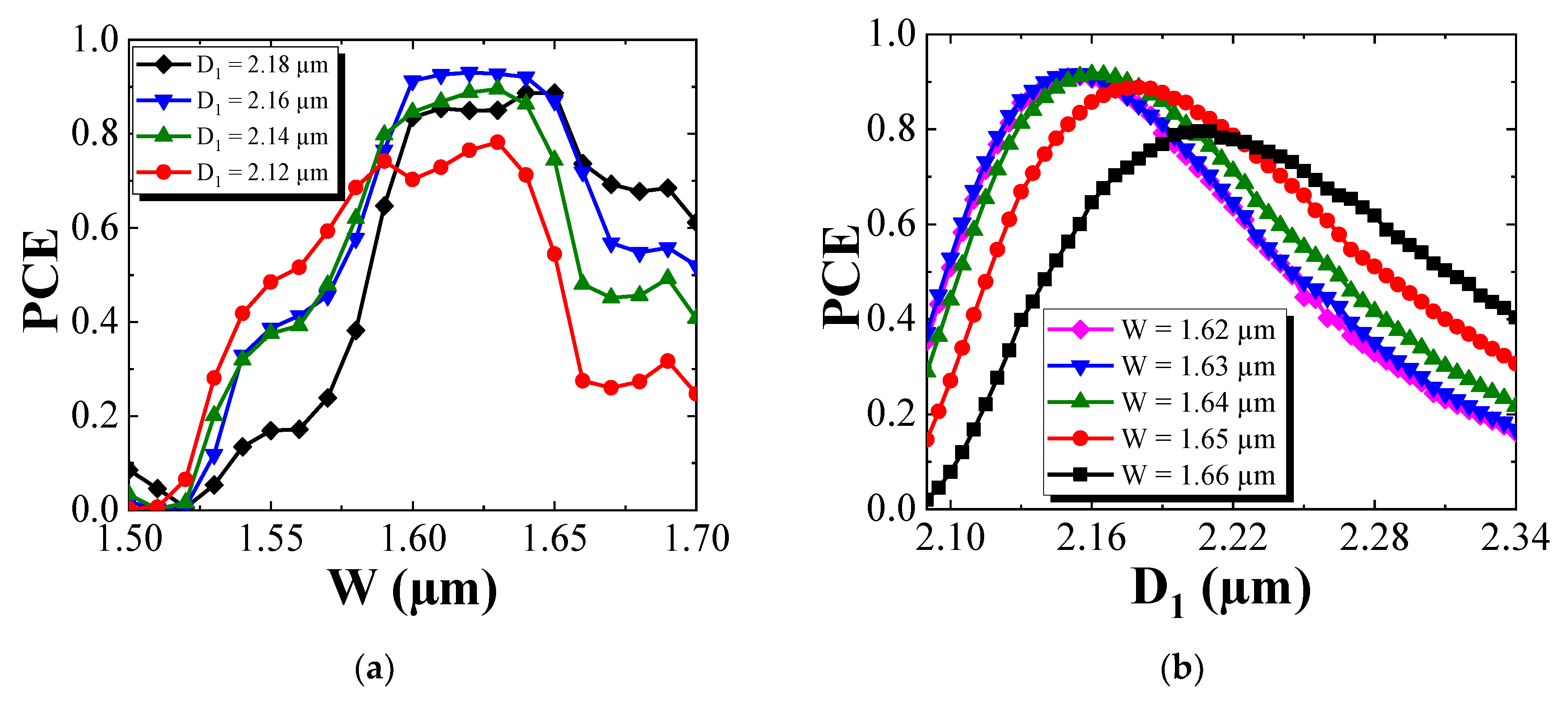
During the fabrication of real devices, process variability results in uncertainties in the values of D1, W, and Lπ. In addition, there are significant tolerances in the epitaxial layer thicknesses in MOVPE, typically of ~5% for bulk layers. The fabrication tolerances therefore need to be investigated. The maximum PCE and half-beat length (Lπ) as D1 changes in steps of 5 nm are shown in Figure 8. With W set to 1.62 μm, the maximum PCE peaked at 92% with D1 = 2.15 μm. For these parameters, the half-beat length was around 1250 μm. With W set to 1.66 μm, the maximum PCE increased to 94% for D1 = 2.25 μm, but Lπ was more than 1800 μm as shown in Figure 8b. Figure 9 shows the variation in maximum PCE and Lπ as a function of W in 10 nm steps. With D1 fixed at 2.16 μm, the maximum PCE was just over 90% over the range of 1.60 μm ≤ W ≤ 1.64 μm. When D1 was increased to 2.18 μm, the maximum PCE changed by less than 5% over the range 1.60 μm ≤ W ≤ 1.64 μm, but Lπ increased to around 1500 μm. For D1 = 2.12 μm, Lπ was reduced to around 1000 μm, but the maximum PCE was less than 90% over the entire range of W. Therefore, to achieve a high PCE with a comparatively short device length, the optimum values of W, D1, and L were 1.62 μm, 2.16 μm, and 1250 μm, respectively.
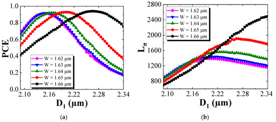
Figure 8.
(a) Maximum PCE and (b) half-beat length, Lπ, as a function of the shallow etched depth D1.
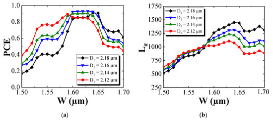
Figure 9.
(a) Maximum PCE and (b) half-beat length, Lπ, as a function of the waveguide width W.
Figure 10 shows the fluctuation of the PCE with respect to W and D1 with the length of the PMC fixed at 1250 μm. To ensure the PCE was more than 85%, which represents a deviation of <8% from the maximum value of 92%, W needed to lie in the range between 1.60 μm and 1.65 μm, and D1 in the range between 2.13 μm and 2.18 μm. Based on the CH4/H2 RIE recipe, the etch rate of AlGaInAs showed a 20-fold reduction compared to that of InP or InGaAsP, so we could achieve precise etch depth control of D1 by using laser interferometry to identify when the top of the MQW waveguide core was reached and then by slowly etching the AlGaInAs layers. Indeed, because of the tolerances in layer thickness associated with MOVPE, it was the position of the etch with respect to the waveguide core that is important rather than the absolute value of D1 measured from the surface.
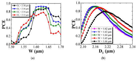
Figure 10.
Maximum PCE with respect to (a) the waveguide width W and (b) the shallow etched depth D1 for a PMC length of 1250 μm.
5. Discussion
Previous researches on MQW-based PMCs have mostly focused on fabricating sources of polarization tunable light, and such sources require the PMC to be integrated with a polarization-dependent phase shifter (PD-PS) [6]. In addition, most reports have used relatively complicated butt-joint integration techniques [16]. The purpose of these polarization tunable sources is to convert pure TE- or TM-polarized light into an arbitrarily chosen state of polarization, and the PMC is required to have a 50% TE-to-TM polarization conversion efficiency [15]. In addition to the birefringence arising from the waveguide geometry, the birefringence of the MQW also affects the polarization conversion in the PMC [6], with the MQW birefringence having the opposite sign to that arising from the asymmetric waveguide. The effect of MQW birefringence is therefore to increase Lπ. In this paper, the PMC used the same epitaxial layer structure as that of an LD, because our target was to monolithically integrate the PMC with a 1.55 µm sidewall-grating distributed-feedback (DFB) laser using QWI to reduce the loss in the PMC [12] and remove the birefringence associated with the MQW stack. As stated in the introduction, QWI has several advantages, including removing the MQW birefringence, reducing the propagation loss, and eliminating the need for regrowth. We have optimized the QWI-based PMC structure to maximize the TE–TM conversion efficiency while minimizing the half-beat length.
We have also modelled the bandwidth of the PMC. Figure 11 presents the PCE as a function of the wavelength, the parameters of the PMC are set up from the profile 2 in Table 2. There is a 25 nm wavelength range where the PCE exceeds 80%, and the maximum PCE is 92.5% (representing an extinction ratio (ER) of 11 dB). These values of PCE and ER are relatively low compared to those of bulk material PMCs reported previously by El-Rafai et al., using a slanted-rib waveguide polarization converters in InGaAsP/InP (97.5% PCE, 16 dB ER) [17], Holmes et al., using asymmetrically etched slots in ridge waveguide polarization converters in GaAs/AlGaAs (96% PCE, 13.8 dB ER) [4], and Elfiqi et al., using a half-ridge InGaAsP/InP design (95% PCE, 12.7 dB ER) [3]. The limited PCE and long length of PMC discussed here is mainly because the epitaxial layer structure was optimized for the LD. For the half-ridge waveguide PMC, the two fundamental eigenmodes’ profiles were largely determined by the structure and refractive index of the core layer, defined by W and D1. PMC with a thicker core layer had a larger optimization range of W and D1. T. Tanemura et al. reported a 500 nm-thick InGaAsP core layer half-ridge waveguide PMC and achieved 16.6 dB ER with a waveguide width of 1 µm and a core layer shallow etched thickness of 200 nm [18]. However, the thickness of the core MQW layer for LD was only 90 nm in our design, leading to three issues: (1) the value of W could not be lower than 1.45 μm, otherwise the two fundamental eigenmodes could not exist, as shown in Figure 4. This reduced the optimization ranges of W and D1 to adjust the maximum PCE; (2) the effective refractive indexes of the TE0 and TM0 modes were quite close, meaning Lπ was relatively long for standard epitaxial structures used for lasers; (3) the thin waveguide core and the resulting low optical confinement reduced the PCE and increased its sensitivity to wavelength variations and fabrication tolerances. The PCE and Lπ values could be improved by optimizing the thickness of the waveguide core to give: (1) a larger propagation constant difference between TE0 and TM0 to reduce Lπ, and (2) higher optical confinement to reduce the sensitivity to input wavelength and PMC dimensions.
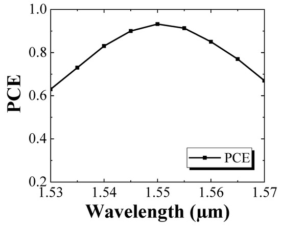
Figure 11.
Maximum PCE as a function of the wavelength.
In addition, using MQW structures and QWI, the scattering loss between the LD and the PMC sections can be reduced significantly compared with a butt joint [10]. The insertion loss for a 1.25 mm-long PMC was calculated to be around 2.27 dB. This includes the 0.05 dB transfer loss from the DFB laser to PMC using a 50 µm-long taper and the additional propagation loss of 2.22 dB due to the deeply etched ridge waveguide [17]. This loss is comparable to that of the bulk material-based PMC reported by Groen et al. (2 dB, 150 μm) [19] and lower than that reported by Elfiqi et al. (4–6 dB, 150 μm) [3].
6. Conclusions
A 1.55 μm AlGaInAs MQW PMC for monolithic integration with an LD using the QWI technique has been designed and optimized. A half-ridge structure was employed to obtain pure TM-polarized light from a TE-polarized input beam. The waveguide width and shallow etched depth of the PMC were investigated and optimized to obtain a high TE–TM conversion efficiency. As a result, an optimized PMC design has been identified, with a waveguide width of 1.62 μm, a shallow etched depth of 2.16 μm, and a length of 1250 μm. With the PMC length fixed at 1250 μm, to guarantee a PCE of more than 85%, the fabricated waveguide width must lie between 1.60 μm and 1.65 μm, and the shallow etched depth between 2.13 μm and 2.18 μm. Compared with the butt-joint and selective area growth PIC techniques, QWI provides a simple, flexible and low-cost approach for integrating an MQW PMC monolithically with an MQW LD and has the additional advantages of reducing parasitic reflections between the two sections, eliminating regrowth and alleviating the birefringence effects associated with MQW structures.
Author Contributions
Conceptualization, J.X., X.L., J.M. and L.H.; Data curation, X.S., B.Q.; Investigation, X.S., S.Y.; Software, X.S.; Writing-original draft preparation, X.S.; Writing- review and editing, J.M., L.H. All authors have read and agreed to the published version of the manuscript.
Funding
This work was supported by the U.K. Engineering and Physical Sciences Research Council (EP/R042578/1) and the Chinese Ministry of Education collaborative project (B17023).
Institutional Review Board Statement
Not applicable.
Informed Consent Statement
Not applicable.
Data Availability Statement
Data available on request due to restrictions e.g., privacy or ethical. The data presented in this study are available on request from the corresponding author. The data are not publicly available as they also form part of an ongoing study.
Acknowledgments
We would like to acknowledge the staff of the James Watt Nanofabrication Centre at the University of Glasgow for help in fabricating the devices and Zhibo Li and Shengwen Xie for their help in Finite-Element Method simulation.
Conflicts of Interest
The authors declare no conflict of interest.
References
- Morsy-Osman, M.; Sowailem, M.; El-Fiky, E.; Goodwill, T.; Hoang, T.; Lessard, S.; Plant, D.V. DSP-free ‘coherent-lite’transceiver for next generation single wavelength optical intra-datacenter interconnects. Opt. Express 2018, 26, 8890–8903. [Google Scholar] [CrossRef] [PubMed]
- Bunandar, D.; Lentine, A.; Lee, C.; Cai, H.; Long, C.M.; Boynton, N.; Martinez, N.; DeRose, C.; Chen, C.; Grein, M. Metropolitan quantum key distribution with silicon photonics. Phys. Rev. X 2018, 8, 021009. [Google Scholar] [CrossRef] [Green Version]
- Elfiqi, A.E.; Kobayashi, R.; Tanomura, R.; Tanemura, T.; Nakano, Y. Fabrication-tolerant half-ridge InP/InGaAsP polarization rotator with etching-stop layer. IEEE Photonics Technol. Lett. 2020, 32, 663–666. [Google Scholar] [CrossRef]
- Holmes, B.; Hutchings, D. Realization of novel low-loss monolithically integrated passive waveguide mode converters. IEEE Photonics Technol. Lett. 2005, 18, 43–45. [Google Scholar] [CrossRef]
- Xie, S.; Andersson, S.M.; Ye, S.; Niu, Z.; Marsh, J.H.; Hou, L. Design of 2 μm Wavelength Polarization Mode Controllers. In Proceedings of the 2020 International Conference on UK-China Emerging Technologies (UCET), Glasgow, UK, 20–21 August 2020; pp. 1–3. [Google Scholar]
- Ito, M.; Okawa, K.; Suganuma, T.; Fukui, T.; Kato, E.; Tanemura, T.; Nakano, Y. Efficient InGaAsP MQW-based polarization controller without active-passive integration. Opt. Express 2021, 29, 10538–10545. [Google Scholar] [CrossRef] [PubMed]
- El-Refaei, H.; Yevick, D. An optimized InGaAsP/InP polarization converter employing asymmetric rib waveguides. J. Lightwave Technol. 2003, 21, 1544–1548. [Google Scholar] [CrossRef]
- Huan, Z.; Scarmozzino, R.; Nagy, G.; Steel, J.; Osgood, R. Realization of a compact and single-mode optical passive polarization converter. IEEE Photonics Technol. Lett. 2000, 12, 317–319. [Google Scholar] [CrossRef]
- Hou, L.; Haji, M.; Dylewicz, R.; Qiu, B.; Bryce, A.C. Monolithic 45-GHz mode-locked surface-etched DBR laser using quantum-well intermixing technology. IEEE Photonics Technol. Lett. 2010, 22, 1039–1041. [Google Scholar] [CrossRef]
- Suzuki, Y.; Iwamura, H.; Miyazawa, T.; Wakatsuki, A.; Mikami, O. Polarization-dependent refractive-index change induced by superlattice disordering. IEEE J. Quantum Electron. 1996, 32, 1922–1931. [Google Scholar] [CrossRef]
- Skogen, E.J.; Raring, J.W.; Barton, J.S.; DenBaars, S.P.; Coldren, L.A. Postgrowth control of the quantum-well band edge for the monolithic integration of widely tunable lasers and electroabsorption modulators. IEEE J. Sel. Top. Quantum Electron. 2003, 9, 1183–1190. [Google Scholar] [CrossRef]
- Walker, R. Simple and accurate loss measurement technique for semiconductor optical waveguides. Electron. Lett. 1985, 21, 581–583. [Google Scholar] [CrossRef]
- Hou, L.; Haji, M.; Akbar, J.; Marsh, J.H.; Bryce, A.C. AlGaInAs/InP monolithically integrated DFB laser array. IEEE J. Quantum Electron. 2011, 48, 137–143. [Google Scholar] [CrossRef]
- Hou, L.; Stolarz, P.; Javaloyes, J.; Green, R.P.; Ironside, C.N.; Sorel, M.; Bryce, A.C. Subpicosecond Pulse Generation at Quasi-40-GHz Using a Passively Mode-Locked AlGaInAs–InP 1.55-μm Strained Quantum-Well Laser. IEEE Photonics Technol. Lett. 2009, 21, 1731–1733. [Google Scholar]
- Zaitsu, M.; Tanemura, T.; Nakano, Y. Numerical study on fabrication tolerance of half-ridge InP polarization converters. IEICE Trans. Electron. 2014, 97, 731–735. [Google Scholar] [CrossRef] [Green Version]
- Hutchings, D.C.; Holmes, B.M. A waveguide polarization toolset design based on mode beating. IEEE Photonics J. 2011, 3, 450–461. [Google Scholar] [CrossRef]
- El-Refaei, H.; Yevick, D.; Jones, T. Slanted-rib waveguide InGaAsP-InP polarization converters. J. Lightwave Technol. 2004, 22, 1352. [Google Scholar] [CrossRef]
- Tanemura, T.; Amemiya, T.; Takeda, K.; Higo, A.; Nakano, Y. Simple and compact InP polarization converter for polarization-multiplexed photonic integrated circuits. In Proceedings of the 2009 IEEE LEOS Annual Meeting Conference Proceedings, Belek-Antalya, Turkey, 4–8 October 2009; pp. 436–437. [Google Scholar]
- Groen, F.; Zhu, Y.; Van Der Tol, J. Compact polarisation converter on InP/InGaAsP using an asymmetrical waveguide. In Proceedings of the 11th European Conference on Integrated Optics (ECIO 2003), Prague, Czech Republic, 2–4 April 2003. [Google Scholar]
Publisher’s Note: MDPI stays neutral with regard to jurisdictional claims in published maps and institutional affiliations. |
© 2021 by the authors. Licensee MDPI, Basel, Switzerland. This article is an open access article distributed under the terms and conditions of the Creative Commons Attribution (CC BY) license (https://creativecommons.org/licenses/by/4.0/).

