Asymmetric Carrier Divider with an Irregular RF Phase on DD-MZ Modulator for Eliminating Dispersion Power Fading in RoF Communication


Abstract
1. Introduction
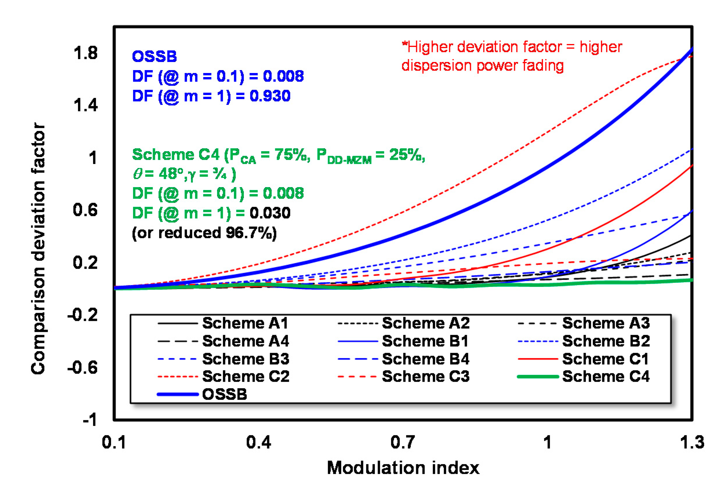
- The laser diode (LD) power (PIN) carrier is divided asymmetrically as the power modulation (PDD-MZM) and carrier arm power (PCA). The power PCA is used to compensate for the power of the carrier of the optical field of the DD-MZM output, which is reduced due to increasing m.
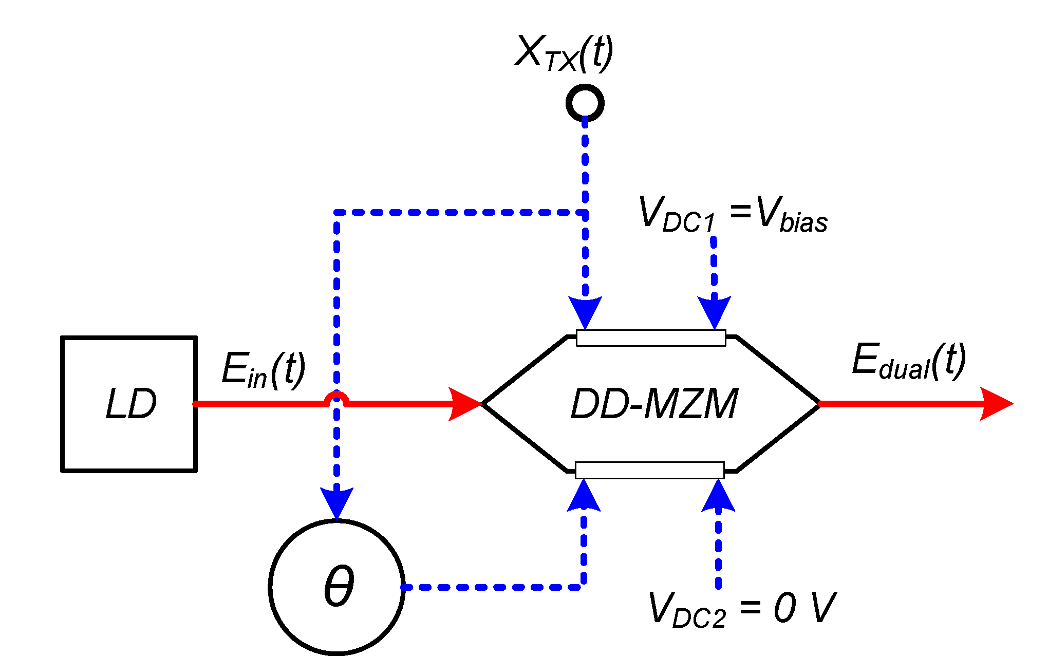
- The RF signal with an irregular phase (θ) was applied to the DD-MZ modulator. Therefore, the optimum EDD-MZM(t) spectrum can be generated by adjusting the DD-MZM arm.
- The minimum DF is obtained when the PIN is separated as 75% for PCA and 25% for PDD-MZM with an irregular RF signal of θ = 48° and bias point value of γ = ¾. This proposed structure produces DF at m = 0.1 and m = 1 value are 0.008 and 0.03, or it reduced DF of 96.7% compared to OSSB.
- The proposed system was successfully applied without additional power or filter, and the additional power or filter managed to increase the cost and complexity of RAP. Moreover, θ is independent of fiber length. Our proposed model is applied for single fiber, not for routing scenarios with many nodes.
- The proposed mathematical model of the system is developed based on the Bessel function. This model can be used to evaluate all the parameters. Furthermore, the model is validated using simulation, and it has very good agreement, which validates the proposed method.
- Nevertheless, the current paper has some limitations: (1) We used the comparison between numerical and simulation models without experiment due to the unavailability of devices, but this model was successfully verified and had a good agreement; (2) Our proposed method was focused on optical signals modulated by RF sine waves [22,26,27,28,29]; (3) To eliminate the dispersion, we focused on the received RF power; (4) We assumed that the optic arm length is less than 1 m; therefore, the phase did not change significantly; (5) In this study, we investigated up to 16 scenarios, and the DD-MZM modulator was used with the best performance in the C4 scenario; and (6) As a consideration, the paper’s proposed method focused not only on asymmetric power divider but also on the optimal phase. Therefore, the minimum DF was obtained by combining the irregular phase and the power divider to reduce DF by 96.7%. We think that the global optimum DF results will also be similar to the proposed case in this scenario. Moreover, we also must consider the availability of the optical divider in the market.
2. Optical Field of DD-MZM Output
2.1. DD-MZM with Basic Configuration
2.2. DD-MZM with Carrier Arm (CA)
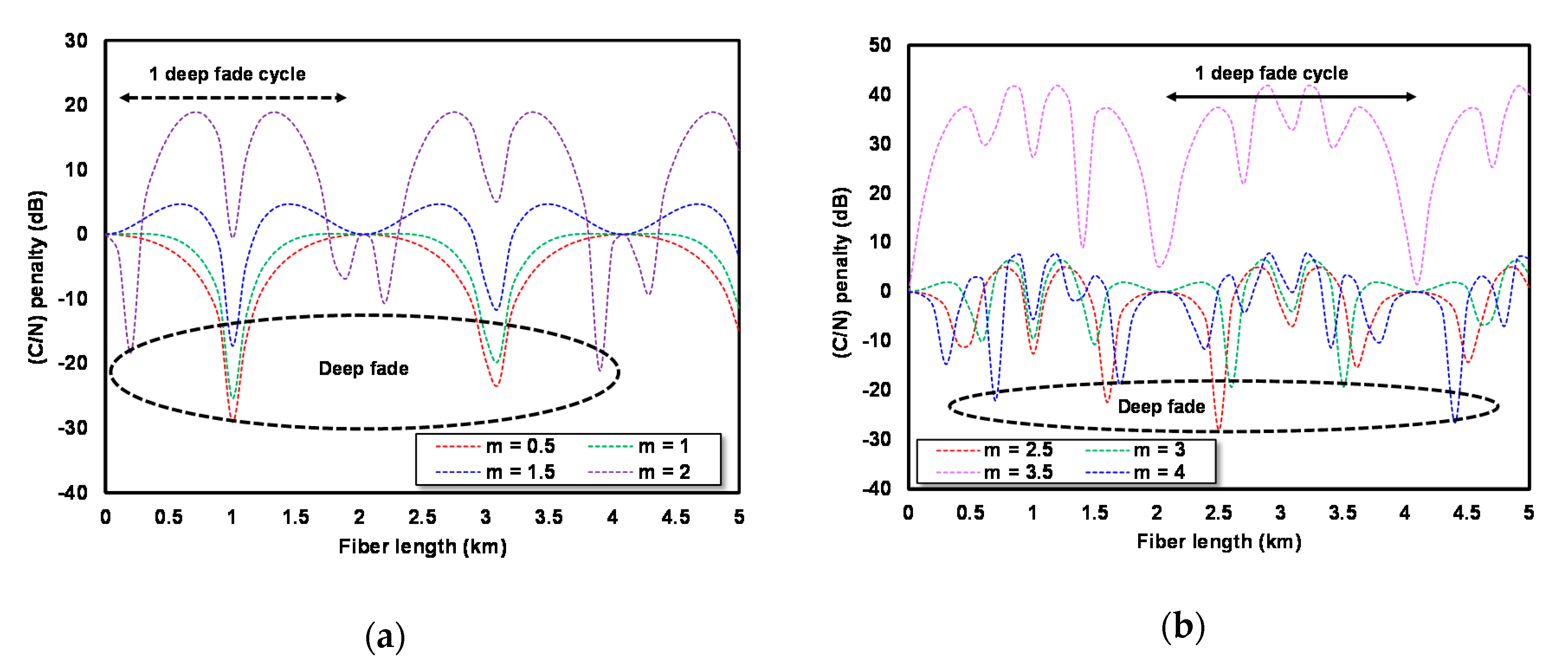
3. C/N Penalty of RoF Link
3.1. C/N Penalty of RoF Link with ODSB Modulation
- (a)
- Calculate Prec(L) using Equation (28) with r = 1 (without CA), Pin = 1 mw (0 dBm), γ = ½, θ = 180°, m = 0.5, λc = 1550 nm (D = 17 ps/(nm.km)), and fm = 60 GHz with L = 0, 0.1, 0.2, … 5 km.
- (b)
- From the obtained Prec(L) in (a), calculate the C/N penalty using Equation (29).
- (c)
- Repeat steps (a) and (b) for m = 1, 1.5, 2, 2.5, 3, 3.5, and 4.
- (d)
- The result of the calculation is shown in Figure 3a,b.
3.2. C/N Penalty of RoF Link with OSSB Modulation
3.3. C/N Penalty of RoF Link with Irregular θ
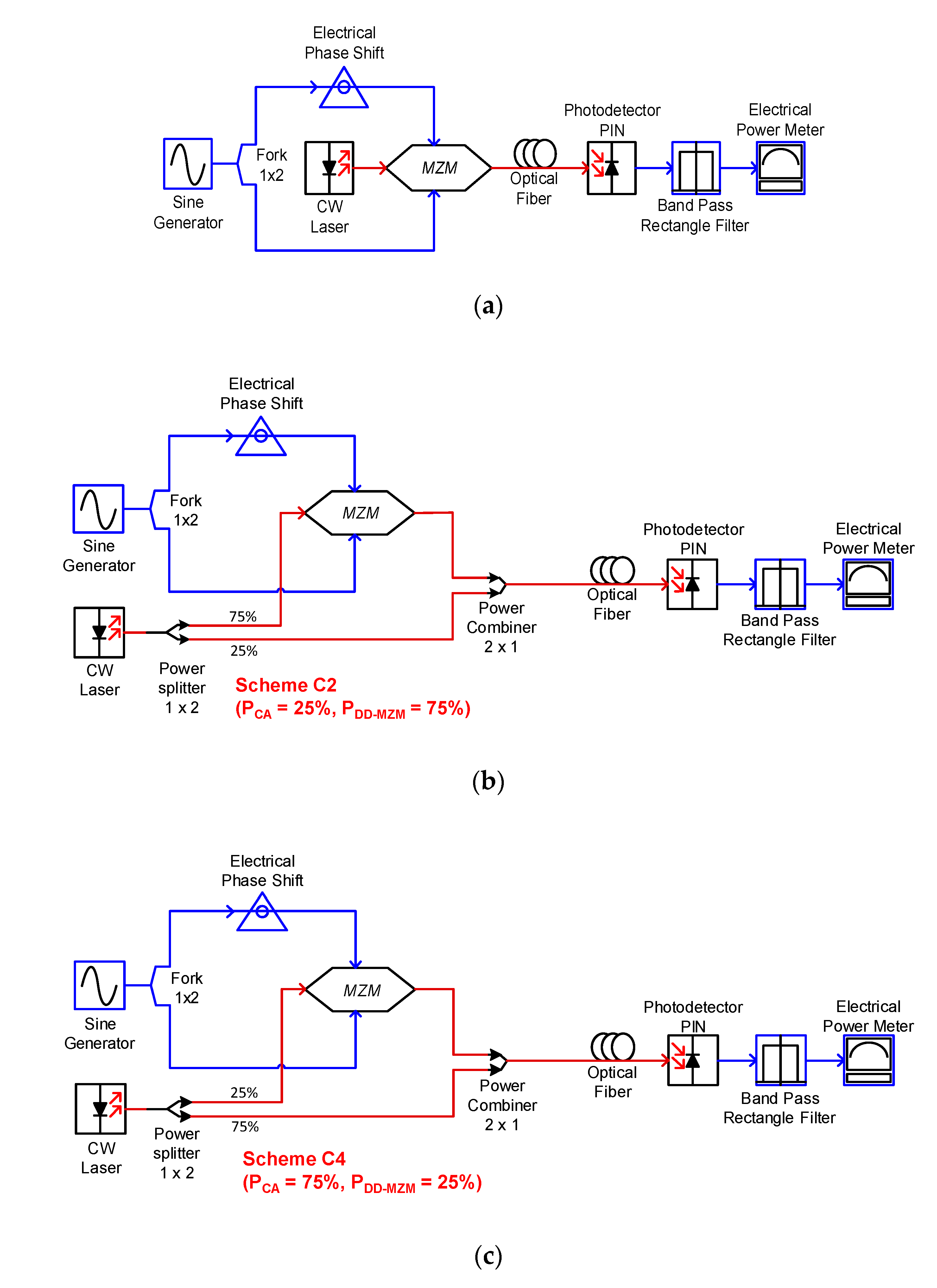
- The whole optical signal power of the LD output is used as the DD-MZM input (basic configuration),
- 75% of the optical signal power generated by LD is used as the DD-MZM input,
- 50% of the optical signal power generated by LD is used as the DD-MZM input, and
- 25% of the optical signal power generated by LD is used as the DD-MZM input,
3.3.1. Irregular θ Values for Scheme A1, A2, A3 and A4
- (a)
- Calculate Prec(L) using Equation (28) with r = 1 (4:4), γ = ¼, m = 0.1, θ = 0°, Pin = 1 mw (0 dBm), λc = 1550 nm (D = 17 ps/(nm.km)), and fm = 60 GHz at L = 0, 0.1, 0.2, …, 5 km.
- (b)
- Calculate the C/N penalty from the calculation results (a) using Equation (29).
- (c)
- Calculate DF of all calculation results of (b) using Equation (30).
- (d)
- Repeat steps (a) to (c) for θ = 1°, 2°, 3°, …, 360°.
- (e)
- Find the θ value in step d), which produces the smallest DF (DFmin); this θ is called irregular θ.
- (f)
- Repeat steps (a) to (e) for m = 0.2, 0.3, …, 4.
- (g)
- The result of the calculation is shown in Figure 5a–d.
3.3.2. Irregular θ Values for Scheme B1, B2, B3 and B4
3.3.3. Irregular θ Values for Scheme C1, C2, C3 and C4
3.3.4. C/N Penalty of the RoF Link with an Irregular θ for All Schemes
4. Numerical Simulation
5. Conclusions
Author Contributions
Funding
Conflicts of Interest
References
- Fernando, X.N. Radio over Fiber for Wireless Communications: From Fundamentals to Advanced Topics; John Wiley & Sons: Hoboken, NJ, USA, 2014. [Google Scholar]
- Insua, I.G. Optical Generation of mm-wave Signals for Use in Broadband Radio over Fiber Systems; Technische Universität Dresden: Dresden, Germany, 2010. [Google Scholar]
- Li, S.; Zheng, X.; Zhang, H.; Zhou, B. Compensation of dispersion-induced power fading for highly linear radio-over-fiber link using carrier phase-shifted double sideband modulation. Opt. Lett. 2011, 36, 546–548. [Google Scholar] [CrossRef] [PubMed]
- Liu, J.; Wu, X.; Huang, C.; Tsang, H.K.; Shu, C. Compensation of Dispersion-Induced Power Fading in Analog Photonic Links by Gain-Transparent SBS. IEEE Photonics Technol. Lett. 2018, 30, 688–691. [Google Scholar] [CrossRef]
- Gao, Y.; Wen, A.; Liu, L.; Tian, S.; Xiang, S.; Wang, Y. Compensation of the Dispersion-Induced Power Fading in an Analog Photonic Link Based on PM–IM Conversion in a Sagnac Loop. J. Light. Technol. 2015, 33, 2899–2904. [Google Scholar] [CrossRef]
- Chen, Z.; Yan, L.; Jiang, H.; Pan, W.; Luo, B.; Zou, X. Dispersion Compensation in Analog Photonic Link Utilizing a Phase Modulator. J. Light. Technol. 2014, 32, 4642–4647. [Google Scholar] [CrossRef]
- Gao, Y.; Wen, A.; Wu, X.; Wang, Y.; Zhang, H. Efficient Photonic Microwave Mixer With Compensation of the Chromatic Dispersion-Induced Power Fading. J. Light. Technol. 2016, 34, 3440–3448. [Google Scholar] [CrossRef]
- Yin, C.; Li, J.; Li, B.; Lv, Q.; Dai, J.; Yin, F.; Dai, Y.; Xu, K. Microwave Photonic Frequency Up-Convertor With Frequency Doubling and Compensation of Chromatic-Dispersion-Induced Power Fading. IEEE Photonics J. 2017, 9, 1–7. [Google Scholar] [CrossRef]
- Tian, Y.; Lee, K.-L.; Lim, C.; Nirmalathas, A. 60 GHz Analog Radio-Over-Fiber Fronthaul Investigations. J. Light. Technol. 2017, 35, 4304–4310. [Google Scholar] [CrossRef]
- Dong, Z. 64QAM Vector Radio-Frequency Signal Generation based on Phase Pre-coding and Optical Carrier Suppression modulation. IEEE Photonics J. 2016, 8, 1. [Google Scholar] [CrossRef]
- Tian, Y.; Lee, K.; Lim, C.; Nirmalathas, A. Experimental Comparison of DSB-SC & OSSB Based 60 GHz Radio-over-Fiber Fronthaul Links. In Proceedings of the 2016 IEEE International Topical Meeting on Microwave Photonics (MWP), Long Beach, CA, USA, 31 October–3 November 2016. [Google Scholar]
- Ma, J.; Yu, J.; Yu, C.; Xin, X.; Zeng, J.; Chen, L. Fiber Dispersion Influence on Transmission of the Optical Millimeter-Waves Generated Using LN-MZM Intensity Modulation. J. Light. Technol. 2007, 25, 3244–3256. [Google Scholar] [CrossRef]
- Yu, J.; Jia, Z.; Yi, L.; Su, Y.; Chang, G.-K.; Wang, T. Optical millimeter-wave generation or up-conversion using external modulators. IEEE Photonics Technol. Lett. 2005, 18, 265–267. [Google Scholar] [CrossRef]
- Wang, K.; Zheng, X.; Zhang, H.; Guo, Y. A Radio-Over-Fiber Downstream Link Employing Carrier-Suppressed Modulation Scheme to Regenerate and Transmit Vector Signals. IEEE Photonics Technol. Lett. 2007, 19, 1365–1367. [Google Scholar] [CrossRef]
- Al-Shareefi, N.A.; Hassan, S.I.S.; Malek, F.; Ngah, R.; Aljunid, S.A. A Study in OCS Millimeter-Wave Generation Using Two Parallel DD-MZMs. In Proceedings of the 2013 IEEE 11th Malaysia International Conference on Communications (MICC), Kuala Lumpur, Malaysia, 26–28 November 2013. [Google Scholar]
- Lim, C.; Tian, Y.; Lee, K.-L.; Nirmalathas, A. Transport Schemes for Fiber-Based Fronthaul for Transporting 60 GHz Wireless Signals. In Proceedings of the 2017 19th International Conference on Transparent Optical Networks (ICTON), Girona, Spain, 2–6 July 2017; pp. 1–4. [Google Scholar]
- Ilgaz, M.A.; Baliž, K.V.; Batagelj, B. A Flexible Approach to Combating Chromatic Dispersion in a Centralized 5G Network. Opto-Electron. Rev. 2020, 28, 35–42. [Google Scholar]
- Ranzini, S.M.; Da Ros, F.; Bülow, H.; Zibar, D. Tunable Optoelectronic Chromatic Dispersion Compensation Based on Machine Learning for Short-Reach Transmission. Appl. Sci. 2019, 9, 4332. [Google Scholar] [CrossRef]
- Parajuli, H.N.; Udvary, E. Novel Vestigial Sideband Modulation Scheme to Enhance the SNR in Radio over Fiber Systems. Radioengineering 2017, 26, 961–967. [Google Scholar] [CrossRef]
- Li, L.; Yi, X.; Song, S.; Chew, S.X.; Minasian, R.A.; Nguyen, L. Microwave Photonic Signal Processing and Sensing Based on Optical Filtering. Appl. Sci. 2019, 9, 163. [Google Scholar] [CrossRef]
- Zheng, Z.; Peng, M.; Zhou, H.; Chen, M.; Jiang, L.; Tan, L.; Dai, X.; Xiang, Y. Optical single sideband millimeter-wave signal generation and transmission using 120° hybrid coupler. Opt. Commun. 2018, 411, 21–26. [Google Scholar] [CrossRef]
- Xue, M.; Pan, S.; Zhao, Y. Optical Single-Sideband Modulation Based on a Dual-Drive MZM and a 120° Hybrid Coupler. J. Light. Technol. 2014, 32, 3317–3323. [Google Scholar] [CrossRef]
- Smith, G.H.; Novak, D.; Ahmed, Z. Overcoming chromatic-dispersion effects in fiber-wireless systems incorporating external modulators. IEEE Transactions Microw. Theory Tech. 1997, 45, 1410–1415. [Google Scholar] [CrossRef]
- Hervé, D.; Corral, J.L.; Fuster, J.M.; Herrera, J.; Martinez, A.; Polo, V.; Ramos, F.; Vourc’h, E.; Marti, J. Techniques for the compensation for chromatic-dispersion effects in fiber-wireless systems. Ursi Radio Sci. Bull. 2004, 26–37. [Google Scholar] [CrossRef]
- Rappaport, T.S. Wireless Communications: Principles and Practice; Prentice Hall PTR: Upper Saddle River, NJ, USA, 1996. [Google Scholar]
- Park, J.; Sorin, W.; Lau, K. Elimination of the fibre chromatic dispersion penalty on 1550 nm millimetre-wave optical transmission. Electron. Lett. 1997, 33, 512. [Google Scholar] [CrossRef]
- Xie, M.; Zhao, M.; Lei, M.; Wu, Y.; Liu, Y.; Gao, X.; Huang, S. Anti-dispersion phase-tunable microwave mixer based on a dual-drive dual-parallel Mach-Zehnder modulator. Opt. Express 2018, 26, 454–462. [Google Scholar] [CrossRef] [PubMed]
- Han, J.; Seo, B.-J.; Han, Y.; Jalali, B.; Fetterman, H. Reduction of fiber chromatic dispersion effects in fiber-wireless and photonic time-stretching system using polymer modulators. J. Light. Technol. 2003, 21, 1504–1509. [Google Scholar] [CrossRef]
- Smith, G.; Novak, D.; Ahmed, Z. Technique for optical SSB generation to overcome dispersion penalties in fibre-radio systems. Electron. Lett. 1997, 33, 74. [Google Scholar] [CrossRef]
- Thomas, V.A.; El-Hajjar, M.; Hanzo, L. Performance Improvement and Cost Reduction Techniques for Radio over Fiber Communications. IEEE Commun. Surv. Tutor. 2015, 17, 627–670. [Google Scholar] [CrossRef]
- Colton, D.; Kress, R. Inverse Acoustic and Electromagnetic Scattering Theory, 3rd ed.; Springer Science & Business Media: Berlin/Heidelberg, Germany, 1998; p. 32. [Google Scholar]
- Ujang, F.; Firmansyah, T.; Priambodo, P.S.; Wibisono, G. Irregular Shifting of RF Driving Signal Phase to Overcome Dispersion Power Fading. Photonics 2019, 6, 104. [Google Scholar] [CrossRef]
- Gliese, U.; Nielsen, S.N.; Nielsen, T. Limitations in distance and frequency due to chromatic dispersion in fibre-optic microwave and millimeter-wave links. In Proceedings of the 1996 IEEE MTT-S International Microwave Symposium Digest, San Francisco, CA, USA, 17–21 June 1996. [Google Scholar]
- Granada, J.; Cárdenas, A.; Guerrero, N. A novel dispersion monitoring technique in W-band radio-over-fiber signals using clustering on asynchronous histograms. Ing. E Investig. 2014, 34, 76–80. [Google Scholar] [CrossRef]
- Davies, R.J. Optical Single Sideband for Broadband and Subcarrier Systems. Doctor of Philosophy; University of Alberta: Edmonton, AB, Canada, 1999. [Google Scholar]
- Meslener, G. Chromatic dispersion induced distortion of modulated monochromatic light employing direct detection. IEEE J. Quantum Electron. 1984, 20, 1208–1216. [Google Scholar] [CrossRef]


| Amplitude | Modulation Index (m) | ||
|---|---|---|---|
| m = 0.1 | m = 1 | m = 2 | |
| Al3 | 0 | 0 | 0.0029 + 0.0029i |
| Al2 | 0 | −0.0026−0.0026i | −0.0079−0.0079i |
| Al1 | −0.0011−0.0011i | −0.0099−0.0099i | −0.013−0.013i |
| AC | 0.0224 + 0.0224i | 0.0172 + 0.0172i | 0.005 + 0.005i |
| Au1 | −0.0011−0.0011i | −0.0099−0.0099i | −0.013−0.013i |
| Au2 | 0 | −0.0026−0.0026i | −0.0079−0.0079i |
| Au3 | 0 | 0 | 0.0029 + 0.009i |
| dBm | 1.015 × 10⁻⁸ | 3.41 × 10⁻⁷ | 4.47 × 10⁻⁹ |
| m | ODSB Modulation | OSSB Modulation | ||
|---|---|---|---|---|
| ∆ C/N Penalty (dB) | DF | ∆ C/N Penalty (dB) | DF | |
| 0.1 | 30.111 | 6.8 | 0.022 | 0.008 |
| 0.5 | 29.046 | 6.5 | 0.560 | 0.202 |
| 1 | 25.455 | 5.5 | 2.507 | 0.930 |
| 1.5 | 21.935 | 4.2 | 7.566 | 2.764 |
| 2 | 40.013 | 10.5 | 19.264 | 4.383 |
| 2.5 | 32.922 | 6.9 | 11.517 | 3.064 |
| 3 | 25.762 | 5.6 | 27.229 | 5.629 |
| 3.5 | 41.870 | 10.8 | 26.272 | 5.207 |
| 4 | 34.368 | 7.4 | 11.525 | 3.773 |
| Bias Point | Power Ratio of PDD-MZM/PIN | |||
|---|---|---|---|---|
| 4:4 | 3:4 | 2:4 | 1:4 | |
| ¼ | Scheme A1 | A2 | A3 | A4 |
| ½ | Scheme B1 | B2 | B3 | B4 |
| ¾ | Scheme C1 | C2 | C3 | C4 |
| m | Scheme A1 | Scheme A2 | Scheme A3 | Scheme A4 | ||||
| θI (deg) | θII (deg) | θI (deg) | θII (deg) | θI (deg) | θII (deg) | θI (deg) | θII (deg) | |
| 0.5 | 136 | 224 | 136 | 224 | 135 | 225 | 135 | 225 |
| 1 | 141 | 219 | 139 | 221 | 137 | 223 | 136 | 224 |
| 1.5 | 147 | 213 | 144 | 216 | 138 | 222 | 136 | 224 |
| 2 | 91 | 269 | 88 | 272 | 138 | 222 | 136 | 224 |
| 2.5 | 64 | 296 | 89 | 271 | 128 | 232 | 135 | 225 |
| 3 | 47 | 313 | 116 | 244 | 98 | 262 | 132 | 228 |
| 3.5 | 53 | 307 | 117 | 243 | 60 | 300 | 119 | 241 |
| 4 | 43 | 317 | 45 | 315 | 160 | 200 | 121 | 239 |
| m | Scheme B1 | Scheme B2 | Scheme B3 | Scheme B4 | ||||
| θI (deg) | θII (deg) | θI (deg) | θII (deg) | θI (deg) | θII (deg) | θI (deg) | θII (deg) | |
| 0.5 | 86 | 274 | 88 | 272 | 90 | 270 | 90 | 270 |
| 1 | 69 | 291 | 83 | 277 | 90 | 270 | 91 | 269 |
| 1.5 | 38 | 322 | 90 | 270 | 96 | 264 | 93 | 267 |
| 2 | 86 | 274 | 115 | 245 | 105 | 255 | 96 | 264 |
| 2.5 | 68 | 292 | 123 | 237 | 111 | 249 | 98 | 262 |
| 3 | 58 | 302 | 67 | 293 | 122 | 238 | 99 | 261 |
| 3.5 | 108 | 252 | 107 | 253 | 68 | 292 | 84 | 276 |
| 4 | 45 | 315 | 46 | 314 | 152 | 208 | 149 | 211 |
| m | Scheme C1 | Scheme C2 | Scheme C3 | Scheme C4 | ||||
| θI (deg) | θII (deg) | θI (deg) | θII (deg) | θI (deg) | θII (deg) | θI (deg) | θII (deg) | |
| 0.5 | 39 | 321 | 315 | 45 | 47 | 313 | 46 | 314 |
| 1 | 26 | 334 | 50 | 310 | 53 | 307 | 48 | 312 |
| 1.5 | 12 | 348 | 86 | 274 | 64 | 296 | 51 | 309 |
| 2 | 71 | 289 | 103 | 257 | 77 | 283 | 55 | 305 |
| 2.5 | 154 | 206 | 103 | 257 | 83 | 277 | 58 | 302 |
| 3 | 156 | 204 | 123 | 237 | 78 | 282 | 65 | 295 |
| 3.5 | 103 | 257 | 102 | 258 | 69 | 291 | 69 | 291 |
| 4 | 101 | 259 | 101 | 259 | 89 | 271 | 78 | 282 |
| Parameter | Value | Units |
|---|---|---|
| Extinction ratio | 60 | dB |
| Switching bias voltage | 4 | V |
| Switching RF voltage | 4 | V |
| Insertion loss | 0 | dB |
| Normalize electrical signal | Unchecked | - |
| Bias voltage1 | 0 | V |
| Bias voltage2 | 2 | V |
| Parameter | Value | Units |
|---|---|---|
| User defined reference wavelength | Checked | - |
| Reference wavelength | 1550 | nm |
| Length | 0–5 | km |
| Attenuation effect | Unchecked | - |
| Group velocity dispersion | Checked | - |
| Third-order dispersion | Unchecked | - |
| Frequency domain parameter | Unchecked | - |
| Dispersion | 17 | ps/nm/km |
Publisher’s Note: MDPI stays neutral with regard to jurisdictional claims in published maps and institutional affiliations. |
© 2020 by the authors. Licensee MDPI, Basel, Switzerland. This article is an open access article distributed under the terms and conditions of the Creative Commons Attribution (CC BY) license (http://creativecommons.org/licenses/by/4.0/).
Share and Cite
Wibisono, G.; Ujang, F.; Firmansyah, T.; S. Priambodo, P. Asymmetric Carrier Divider with an Irregular RF Phase on DD-MZ Modulator for Eliminating Dispersion Power Fading in RoF Communication. Photonics 2020, 7, 106. https://doi.org/10.3390/photonics7040106
Wibisono G, Ujang F, Firmansyah T, S. Priambodo P. Asymmetric Carrier Divider with an Irregular RF Phase on DD-MZ Modulator for Eliminating Dispersion Power Fading in RoF Communication. Photonics. 2020; 7(4):106. https://doi.org/10.3390/photonics7040106
Chicago/Turabian StyleWibisono, Gunawan, Febrizal Ujang, Teguh Firmansyah, and Purnomo S. Priambodo. 2020. "Asymmetric Carrier Divider with an Irregular RF Phase on DD-MZ Modulator for Eliminating Dispersion Power Fading in RoF Communication" Photonics 7, no. 4: 106. https://doi.org/10.3390/photonics7040106
APA StyleWibisono, G., Ujang, F., Firmansyah, T., & S. Priambodo, P. (2020). Asymmetric Carrier Divider with an Irregular RF Phase on DD-MZ Modulator for Eliminating Dispersion Power Fading in RoF Communication. Photonics, 7(4), 106. https://doi.org/10.3390/photonics7040106