Article

Terahertz Emission Spectroscopy and Microscopy on Ultrawide Bandgap Semiconductor β-Ga2O3

1
Institute of Laser Engineering, Osaka University, Osaka 565-0871, Japan
2
SCREEN Holdings CO., Ltd., Kyoto 612-8486, Japan
3
Graduate School of Energy Science, Kyoto University, Kyoto 606-8501, Japan
*
Author to whom correspondence should be addressed.
Photonics 2020, 7(3), 73; https://doi.org/10.3390/photonics7030073
Submission received: 18 August 2020 / Revised: 9 September 2020 / Accepted: 11 September 2020 / Published: 14 September 2020

Abstract

:
Although gallium oxide Ga2O3 is attracting much attention as a next-generation ultrawide bandgap semiconductor for various applications, it needs further optical characterization to support its use in higher-performance devices. In the present study, terahertz (THz) emission spectroscopy (TES) and laser THz emission microscopy (LTEM) are applied to Sn-doped, unintentionally doped, and Fe-doped β-Ga2O3 wafers. Femtosecond (fs) laser illumination generated THz waves based on the time derivative of the photocurrent. TES probes the motion of ultrafast photocarriers that are excited into a conduction band, and LTEM visualizes their local spatiotemporal movement at a spatial and temporal resolution of laser beam diameter and a few hundred fs. In contrast, one observes neither photoluminescence nor distinguishable optical absorption for a band-to-band transition for Ga2O3. TES/LTEM thus provides complementary information on, for example, the local mobility, surface potential, defects, band bending, and anisotropic photo-response in a noncontact, nondestructive manner. The results indicated that the band bends downward at the surface of an Fe-doped wafer, unlike with an n-type wafer, and the THz emission intensity is qualitatively proportional to the product of local electron mobility and diffusion potential, and is inversely proportional to penetration depth, all of which have a strong correlation with the quality of the materials and defects/impurities in them.

Graphical Abstract

1. Introduction

Gallium oxide (Ga2O3) is an attractive ultrawide-bandgap semiconductor for the use in a variety of applications such as gas sensors, high-power electronics, and deep-ultraviolet (UV) photo-detectors [1,2,3]. In recent years, tremendous efforts have been made to improve material quality and device performance. However, there remain many unsolved problems in the areas of defect reduction, passivation improvement, impurity-doping, device processes, carrier dynamics, etc. Contributions to resolve these issues require a new type of characterization tool, particularly one that operates in a noncontact, nondestructive manner. Terahertz (THz) emission spectroscopy (TES) and laser THz emission microscopy (LTEM) are emerging technologies that can detect ultrafast photocarrier dynamics and responses in materials and devices [4,5] that are affected by electron mobility, surface potential, defects, and band bending.
Femtosecond (fs) laser illumination to materials generates THz waves due to the charge displacement that occurs when the photons create free carriers, or when the materials have nonlinear optical coefficients. In the former case, excitation via acceleration due to the built-in field inside the material or carrier diffusion due to a concentration gradient causes excited electrons to translate rapidly and generate transient photocurrents, which are the source of THz radiation. The THz waveforms monitored in the time domain include early-stage carrier dynamics information on a time scale of less than a picosecond. The dynamics-related information provided is different from that provided by typical photoluminescence, electroluminescence, and laser-induced photocurrent characterization methods [6]. We have reported several examples in which defect analysis [7], noncontact surface potential estimation [8,9], and nondestructive evaluation of solar cells [10] are demonstrated and shown that TES and LTEM are practical tools for semiconductor research and development. In the present study, we employ TES and LTEM to study local ultrafast photocarrier dynamics in β-Ga2O3, which has an ultrawide bandgap of approximately 4.7–4.9 eV [3,11,12,13]. As discussed later, the wide bandgap semiconductors have narrow depletion layers with large surface potentials, which mean that the THz emission strongly depends on the surface conditions and the dynamic behavior of the excited carriers. Such information is essential to develop high-performance devices.

2. Terahertz Emission from Semiconductor Surfaces

Photons with energies larger than the bandgap create electron–hole pairs within the optical penetration depth. The primary mechanism of THz wave generation in standard and widegap semiconductors is attributed to the drift current generated by carrier acceleration from the built-in field, whereas wave generation in narrow bandgap semiconductors is explained by ballistic hot carrier diffusion [14,15]. The drift current is defined primarily by the built-in field, carrier mobility, and the number of photocarriers. Here, one can assume that the only electrons contribute to generate the THz waves, and the built-in field is approximated by the field at the surface E Max . The THz amplitude E THz is then written as [16]
E T H z J t Δ n Δ v Δ t   μ e E M a x I P
where J is photocurrent, Δ n is the number of the excited carrier, Δ v is the carrier velocity after the transient time Δ t , which is typically less than 500 fs, μe is the electron mobility and I P is the number of photons injected. When the optical penetration depth λ L is close to or longer than the depletion layer thickness w , this can be simplified as [16]
E T H z   ± μ e ϕ D λ L I P ,
where ϕ D is the diffusion potential. The sign changes with the sign of the potential. This formula indicates that TES includes information on the photocarrier mobility and traveling direction, defects close to the surface, and impurities at a resolution similar to that of the laser spot size. Thus, one can interrogate such physics by combining TES/LTEM results with those from other characterization tools such as the Kelvin force microscope (KFM), photoluminescence (PL), Raman spectroscopy, and optical absorption.

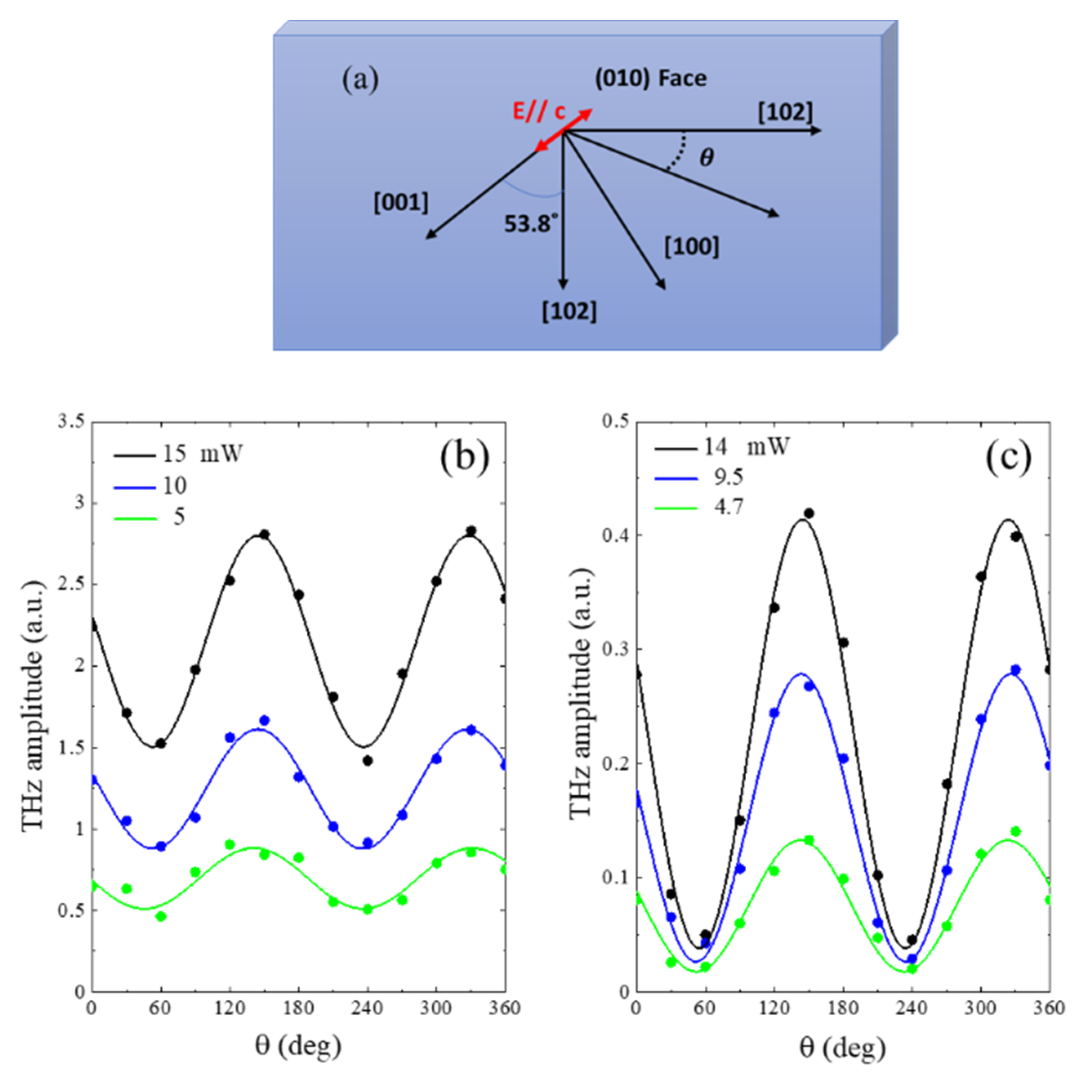
3. Samples and Experiments

The five types of β-Ga2O3 crystals examined here are Sn-doped (010), Sn-doped ( 2 ¯ 01 ), unintentionally doped (UID) (010), UID ( 2 ¯ 01 ), and Fe-doped (010), which were grown by Tamura Corporation using edge-defined film-fed growth, and are labeled as #SnD-1, #SnD-2, #UID-1, #UID-2, and #FeD, respectively. The UV-vis absorption study and terahertz time domain spectroscopy have been reported in [17,18]. The sample specifications are listed in Table 1, together with other information such as electron mobility, surface potential ϕ S , and dielectric constants from the literature [19,20,21,22,23] and our estimates of depletion layer thickness w , E Max , and | μ e ϕ D λ L | . It is worth noting that the thickness of the depletion layers is in the order of 100 nm or shorter.
Figure 1 shows the schematics of typical n-type and semi-insulating Ga2O3 energy band structures. Ga2O3 has various types of defects, such as oxygen vacancies, Ga vacancies, and their complexes. There exist many levels, such as those from self-trapped holes, self-trapped excitons, and shallow donors Sn and Si in n-type samples. These have activation energies from a few meV to several tens of meV [22,24,25]. Although the information on Fe-doped Ga2O3 remains limited, the Fermi energy is pinned at Ec-0.85 eV due to its deep acceptors [26]. However, no clear picture of the energy band structure near the surface of Fe-doped β-Ga2O3 crystals has been provided thus far. Therefore, there are two possibilities as depicted in Figure 1b. One is similar to that of an n-type semiconductor, while the other is similar to that of Fe-doped InP. These two possibilities would cause positive and negative diffusion potentials, respectively. We examine this question for the present case. The optical penetration depth at a photon energy of 4.8 eV is estimated to be approximately 125 nm based on the absorption measurement in [27]. Thus, Equation (1) is always valid. Photoluminescence spectra for all samples are given in the Supplemental Material.
Figure 2a shows an experimental setup for the THz emission measurements. A Ti:sapphire femtosecond laser (pulse width: 100 fs, center wavelength: 800 nm, repetition rate: 80 MHz) is used as a laser source. The femtosecond laser pulses are divided into pump pulses and trigger pulses by using a beam splitter. To generate THz pulse, the surfaces of the samples are irradiated with the pump pulses at an incidence angle of 45 degrees through an optical lens, and the radiated terahertz waves are detected at an opposing 45 degrees angle of emission. The samples are mounted on computer-controlled x-y stage. The PL detector is placed at 90 degrees of prospect angle to the surface. The schematic drawing of those geometries is given in Figure 2b. The emitted THz waves are collimated and focused onto a detector by a pair of parabolic mirrors. We use a spiral type photoconductive antenna (PCA) fabricated on the low-temperature-grown (LTG) GaAs substrate (Hamamatsu Photonics) to detect the THz waves. THz signals in time-domain are acquired by varying the delay between the pump and trigger pulses. The amplitude of the THz wave emission is monitored using a lock-in amplifier. By fixing the time delay at the maximum amplitude of the THz emission and scanning the sample by the pump beam, the THz emission image can be obtained. The laser beam diameters for TES and LTEM/PL are 500 mm and 50 mm, respectively. The details are reported elsewhere [20,30,31,32].

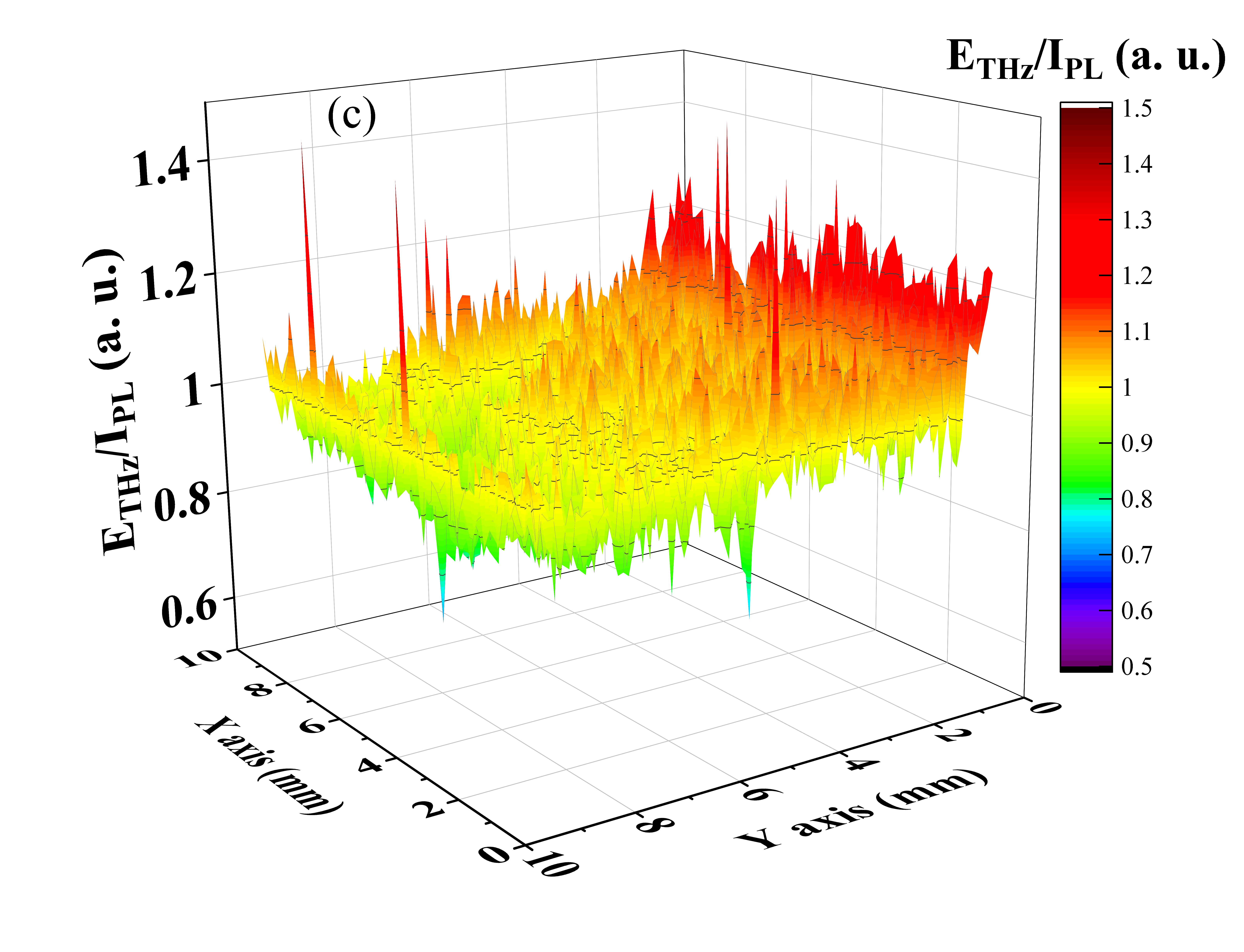
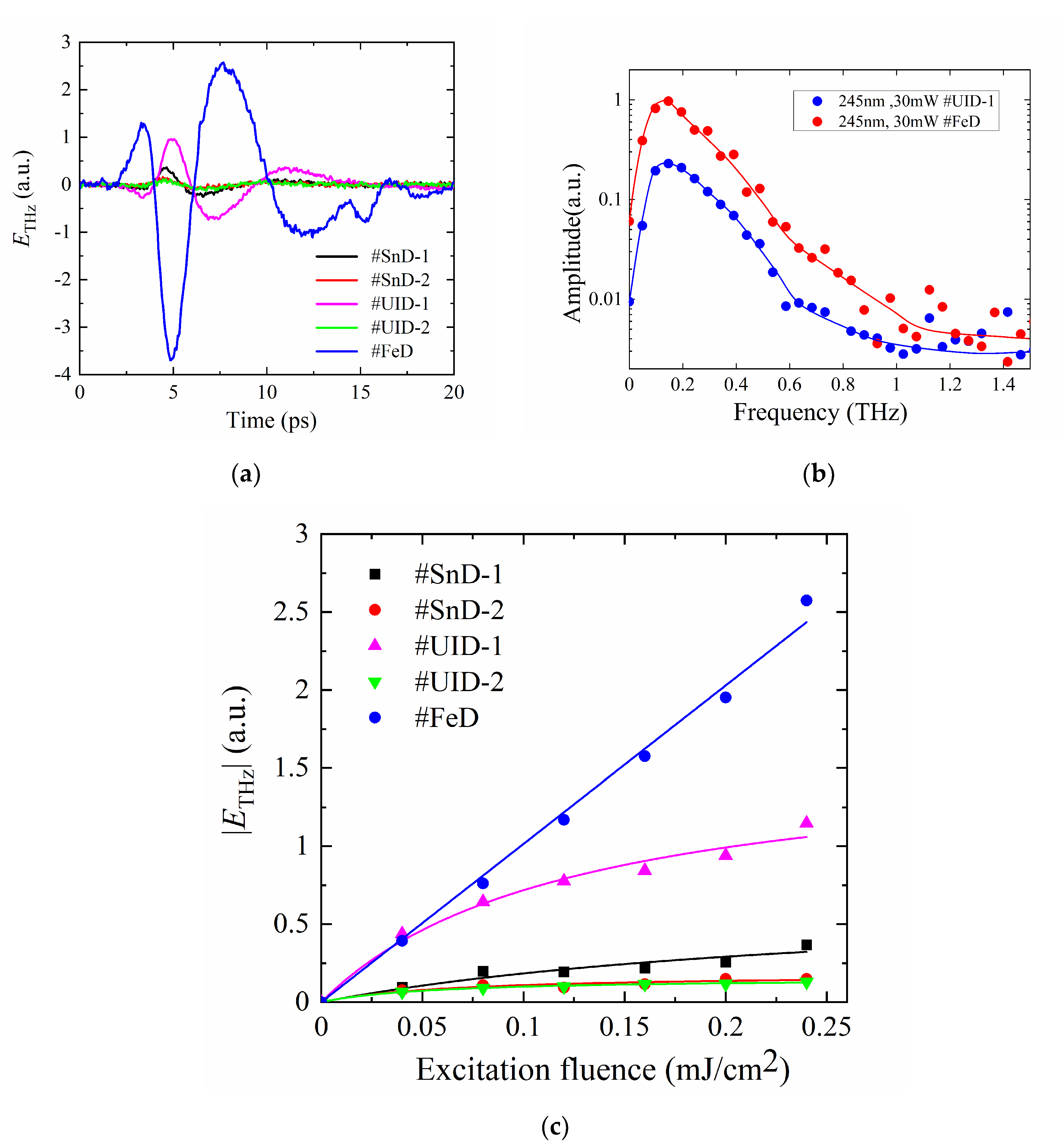
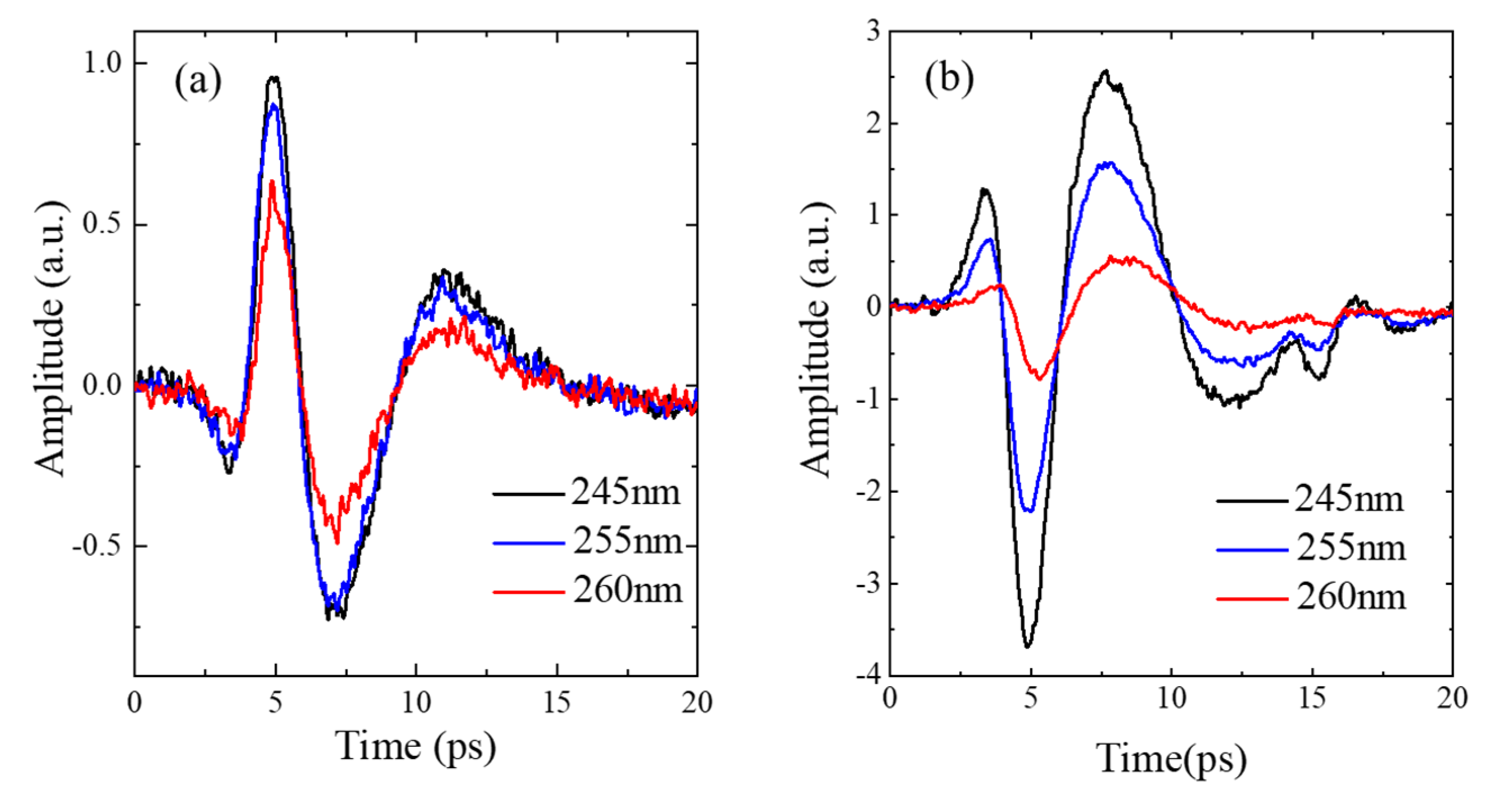
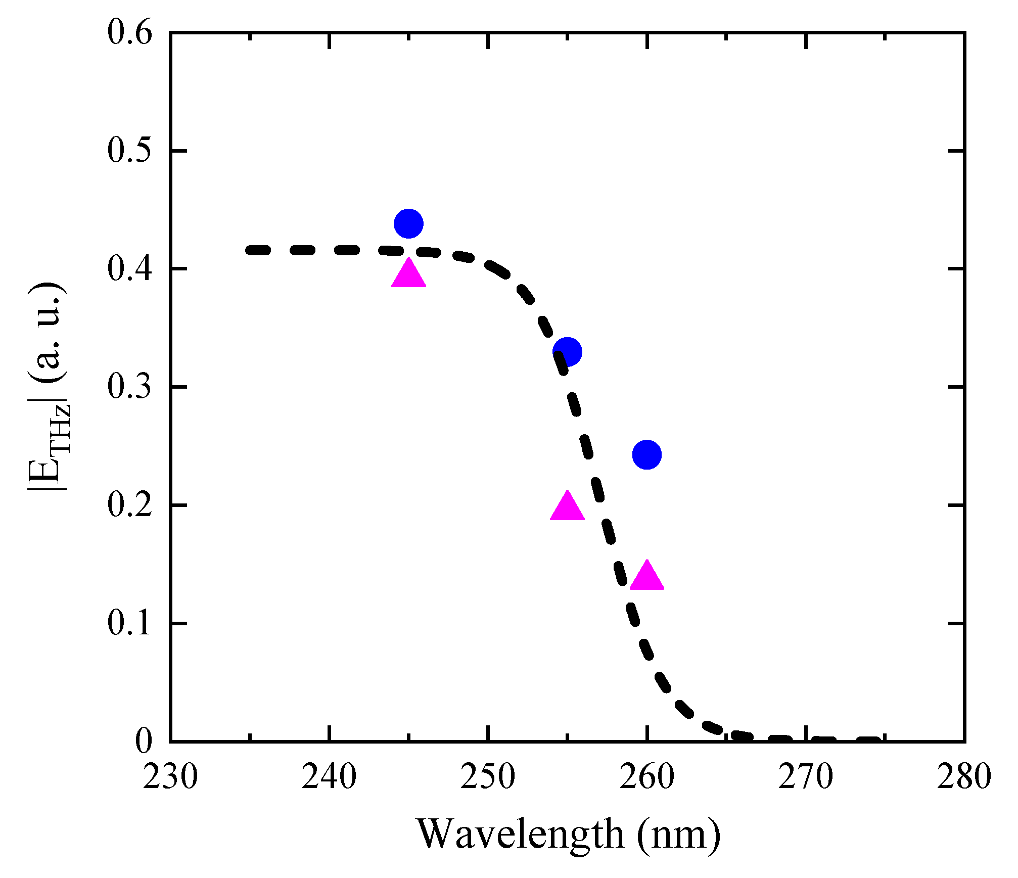
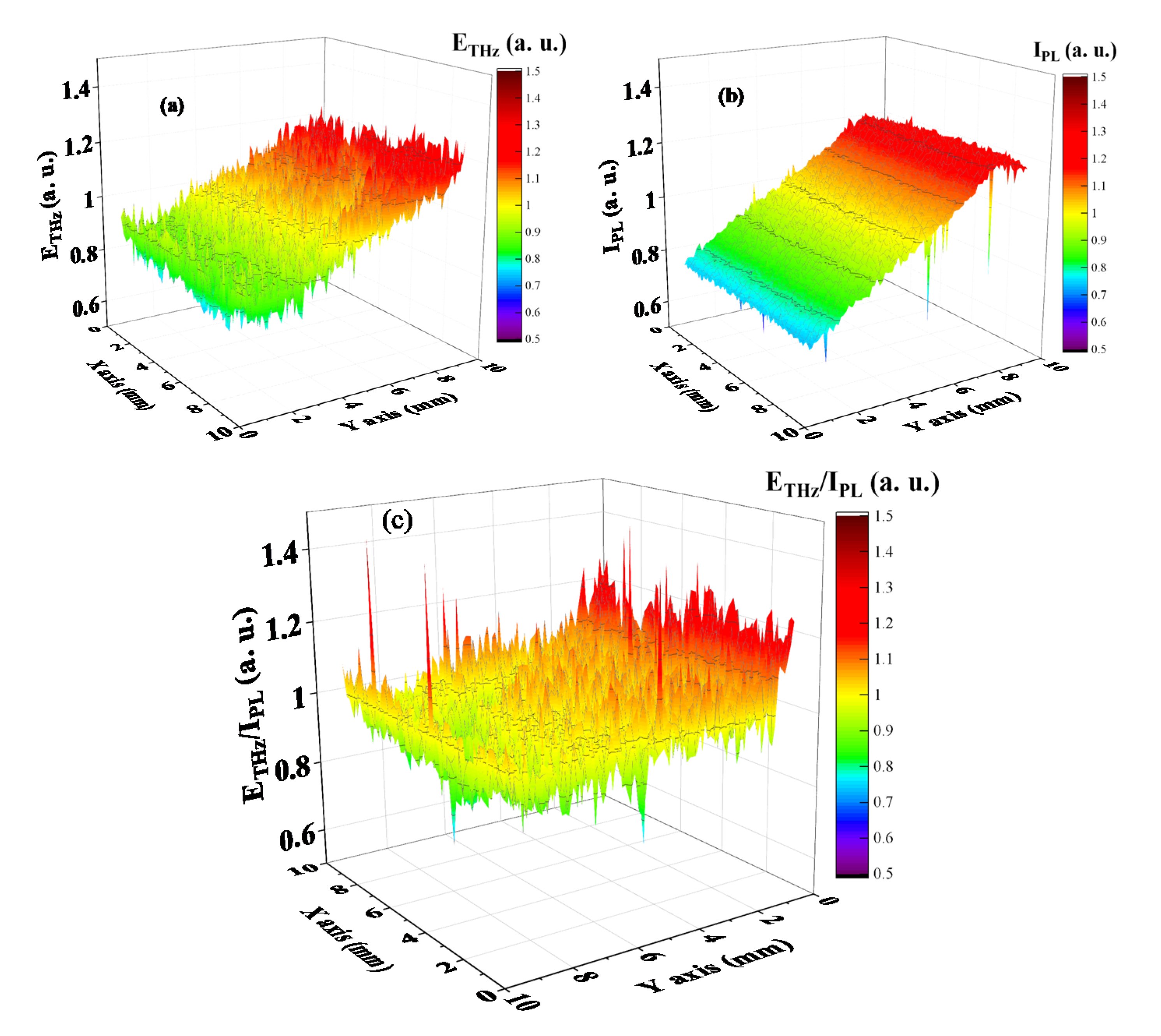
4. Results and Discussion

Figure 3 shows the THz emission properties of β-Ga2O3. We observe THz emissions from all of the samples that we examined, although their amplitudes differ substantially. The sign of the amplitude of #FeD is opposite those of the doped samples. This indicates that the excited electrons in the doped samples travel inward to the substrates, whereas those in #FeD travel to the surface. This answers the first question for the surface diffusion potential of the Fe-doped β-Ga2O3 by clarifying that the conduction band near the surface of #FeD bends downward. After the main pulses, there are certain differences, which is attributed to the charge oscillation near the surfaces related to the capacitance of the depletion layers. In the Fourier spectra, the lower frequency components are enhanced because we used the spiral type PCAs. Since the electromagnetic waves propagate along the edge of the antenna, resulting in the integration of the waveform in time domain [33,34], we cannot discuss the intrinsic carrier dynamics in the β-Ga2O3 with the frequency spectra.
Sample #FeD is found to emit the strongest THz radiation at high influences. At low fluences, its emission is similar to that of #UID-1. The amplitudes of samples other than #FeD increase with saturation. This is often explained by the screening effect [35]. Since the electrons and holes move in opposite directions in the depletion layer, the built-in field is screened. The fits are obtained using the screening effect formula, E THz = (E0F)/(F + Fsat), where E THz is the amplitude of THz radiation, E0 is the THz amplitude at the high fluence limit, F is the optical fluence, and Fsat is the saturation fluence. The estimated values for E0 and Fsat are listed in the Table 2. However, those parameters include no important physical meaning because the emission mechanism is complicated in the case of the semiconductor surface. For instance, #FeD exhibits complex dynamics. On the one hand, the depletion layer of #FeD is thicker than those of the doped samples. This produces a weaker E Max . On the other hand, μ e is expected to be high because of the lower free electron scattering rate. Furthermore, the Fe acceptors capture electrons from point defect donors, which may be excited. The excited electrons are blocked at the surface, while those in the doped materials can travel inward. All of these issues affect the dynamic screening effect and should be examined via more precise models and time-domain simulations with a Monte Carlo simulation considering real parameters.
The wavelength dependences of the waveforms are depicted in Figure 4. As the photon energy crossing the bandgap increases, one can clearly see THz emission enhancement. TES thus discloses the ultrafast nature of the photocarriers excited from the valence band to the conduction band. Note that the PL and optical absorption measurements merely show the direct band-to-band transitions. The PL results are given in Figure S1 in the Supplementary Material. Details of these dynamics are discussed in later sections. Although weak emission is observed below the bandgap, this is explained by wavelength broadening due to the short pulse width of the fs laser.
The maximum intensities of E THz for #UID-1 and #FeD are plotted at the measured three wavelengths in Figure 5. Here to avoid the strong screening effect, the amplitudes measured at a laser fluence of 0.04 mJ/cm2 are used. The intensity increases rapidly with decreasing wavelength. The transition is explained by the broadening of the fs optical pulses. The laser pulse, in general, is regarded to have a shape of hyperbolic secant function, and wavelength ( λ )-dependent laser intensity I P ( λ ) is expressed by
I P ( λ )   sech 2 ( A ( λ λ P ) ) ,
where λ P is the center wavelength of the laser, and A is a fitting parameter corresponding to the pulse width. Thus, the intensity of E THz is expressed by
| E T H z |   I P 0 λ g sech 2 ( A ( λ λ P ) ) d λ ,
where λ g is the bandgap wavelength of the laser. The broken line in Figure 4 is the fit to the experimental data of | E THz | with A of 0.25 assuming the wavelength width of 7 nm at a half maximum for λ g of 257 nm, which corresponds to an energy of 4.82 eV. The value agrees with the β-Ga2O3 bandgap energy. The fit quantitatively explains that the THz emission amplitudes are defined by the number of the photocarriers excited into the conduction bands, i.e., THz waves are emitted by the photocarrier excitation. In other words, for the present case, the THz emission spectroscopy is a direct local measure of the Ga2O3 bandgap for the surface layer within a thickness of about 100 nm.
The anisotropic bandgap of (010) β-Ga2O3 has been reported by observing the anisotropic optical absorption with the polarization of the laser [17]. Thus it is expected that the THz emission amplitude depends on the polarization of the fs laser. Figure 6 gives the optical polarization angle dependence of the emission amplitude. We observed the sinusoidal modulation of the THz emission amplitudes. Here, we rotate the pump polarization angle α from 0° to 360° (0° and 90° correspond to p- and s-polarization, respectively) using a half-wave plate instead of rotating the sample to keep the THz E field always aligned in the same direction to the detector. Note that the spiral PCA has a strong anisotropic response function to the THz E-field. Typically, this modulation is explained by nonlinear THz generation through optical rectification (OR) based on the second-order nonlinear optical susceptibility, which is observed in many semiconductors [36]. However, (010) β-Ga2O3 has the centrosymmetric plain [3], and no strong THz generation due to the second order nonlinear susceptibility is expected [37]. In addition. A small wavelength change on the order of a few nm strongly modulates the THz amplitude. Thus, one can conclude that TES can measure the anisotropic bandgap of β-Ga2O3 directly.
The built-in surface field of doped Ga2O3 is much larger than those of conventional semiconductors. The field E Max is roughly estimated by dividing ϕ D by the depletion layer thickness w , which is defined by,
w   =   2 ε r ε 0 ϕ D e N D  
where ϕ D of a doped semiconductor can be approximated by the surface potential measured values via KFM. The values of w are typically about 100 nm or less, which results in built-in fields that are much stronger than those of the conventional semiconductors [38]. As given in Equation (2), the emission amplitude is proportional to | μ e ϕ D λ L | . All these parameters are intricately related to each other with the surface states and impurities near the surfaces. The parameters discussed above are listed in Table 1. They suggest that #UID-1 has the strongest emission of the doped Ga2O3 samples. The values agree quantitatively with the intensities observed in Figure 2. The results indicate that TES is a useful tool for nondestructive, noncontact analysis of the local electron mobility, surface potential, defects, etc.
Finally, we evaluate the #UID-1 wafer by LTEM. With a beam diameter of 50 µm at an fs laser power of 50 mW, we scanned the laser beam on #UID-1 for a 5 mm × 5 mm area. The LTEM and PL images are given in Figure 7a and 7b, respectively. The PL image was obtained at an fs laser power of 20 mW at a wavelength of 365 nm, which corresponds to the UV luminescence as described in Figure 1a [39]. Both images show a similar intensity distribution. The distribution is possibly attributed to the sample holder tilt. The LTEM image of the normalized intensity divided by the PL intensity is shown in Figure 7c. This suggests that the LTEM image corresponds to almost the self-trapped hole distribution. A faint feature is also seen in the LTEM image, which might be caused by the surface scratch marks.

5. Conclusions

In summary, TES and LTEM have been applied to β-Ga2O3. The polarity change in the THz amplitude revealed that the band near the surface of Fe-doped β-Ga2O3 bends downward, unlike similar bands in n-type materials. It was also found that the emission intensity from the n-type β-Ga2O3 samples was proportional to | μ e ϕ D λ L | . The wavelength and polarization dependences of the THz emission also confirmed that anisotropic optical excitation from the valence to the conduction band played an essential role in THz emission. It is also shown that the LTEM visualizes the self-trapped hole and a faint surface potential distribution. These results have proven that TES and LTEM provide local information on the mobility, surface potential, defects, and anisotropic photoresponse within the diameter of the fs laser beam in a nondestructive, noncontact manner. PL and UV-vis sometimes provide less information on band-to-band transitions [40,41]. Thus, one can probe local ultrafast photocarrier dynamics by combining TES/LTEM with other characterization techniques such as KFM, nano-Raman spectroscopy, nano-PL, and pump-and-probe measurements [42]. This is essential to semiconductor research and development, especially with regard to wide bandgap semiconductors [43].

Supplementary Materials

The following are available online at https://www.mdpi.com/2304-6732/7/3/73/s1, Figure S1: Photoluminescence of each sample.

Author Contributions

I.K. and M.T. conceptualized the work; H.J., C.G., and T.N. carried out the terahertz measurements; all authors (H.J., C.G., T.N., H.M., I.K., H.N., M.T.) discussed the results; H.J. and M.T. analyzed data and wrote the paper; I.K. and H.N. commented on the manuscript. All authors have read and agreed to the published version of the manuscript.

Funding

This work was partially supported by JSPS KAKENHI, Grant Numbers JP18KK0140, and JP18K18861.

Conflicts of Interest

The authors declare no conflict of interest.

References

  1. Ahmadi, S.E.; Oshima, Y. Materials issues and devices of α-and β-Ga2O3. J. Appl. Phys. 2019, 126, 160901. [Google Scholar] [CrossRef] [Green Version]
  2. Pearton, S.J.; Ren, F.; Tadjer, M.; Kim, J. Perspective: Ga2O3 for ultra-high power rectifiers and MOSFETS. J. Appl. Phys. 2018, 124, 220901. [Google Scholar] [CrossRef] [Green Version]
  3. Higashiwaki, M.; Sasaki, K.; Murakami, H.; Kumagai, Y.; Koukitu, A.; Kuramata, A.; Masui, T.; Yamakoshi, S. Recent progress in Ga2O3 power devices. Semicond. Sci. Technol. 2016, 31, 034001. [Google Scholar] [CrossRef]
  4. Rana, D.S.; Tonouchi, M. Terahertz Emission Functionality of High-Temperature Superconductors and Similar Complex Systems. Adv. Opt. Mater. 2020, 8, 1900892. [Google Scholar] [CrossRef]
  5. Huang, Y.; Yao, Z.; He, C.; Zhu, L.; Zhang, L.; Bai, J.; Xu, X. Terahertz surface and interface emission spectroscopy for advanced materials. J. Phys. Condens. Matter. 2019, 31, 153001. [Google Scholar] [CrossRef]
  6. Nakanishi, H.; Ito, A.; Takayama, K.; Kawayama, I.; Murakami, H.; Tonouchi, M. Comparison between laser terahertz emission microscope and conventional methods for analysis of polycrystalline silicon solar cell. AIP Adv. 2015, 5, 117129. [Google Scholar] [CrossRef]
  7. Sakai, Y.; Kawayama, I.; Nakanishi, H.; Tonouchi, M. Polarization imaging of imperfect m-plane GaN surfaces. APL Photonics 2017, 2, 041304. [Google Scholar] [CrossRef] [Green Version]
  8. Mochizuki, T.; Ito, A.; Mitchell, J.; Nakanishi, H.; Tanahashi, K.; Kawayama, I.; Tonouchi, M.; Shirasawa, K.; Takato, H. Probing the surface potential of oxidized silicon by assessing terahertz emission. Appl. Phys. Lett. 2017, 110, 163502. [Google Scholar] [CrossRef]
  9. Mochizuki, T.; Ito, A.; Nakanishi, H.; Tanahashi, K.; Kawayama, I.; Tonouchi, M.; Shirasawa, K.; Takato, H. Noncontact evaluation of electrical passivation of oxidized silicon using laser terahertz emission microscope and corona charging. J. Appl. Phys. 2019, 125, 151615. [Google Scholar] [CrossRef]
  10. Nakanishi, H.; Fujiwara, S.; Takayama, K.; Kawayama, I.; Murakami, H.; Tonouchi, M. Imaging of a polycrystalline silicon solar cell using a Laser Terahertz Emission Microscope. Appl. Phys. Express. 2012, 5, 112301. [Google Scholar] [CrossRef]
  11. Orita, M.; Ohta, H.; Hirano, M. Deep-untravioletteansparent conductive β-Ga2O3 thin films. Appl. Phys. Lett. 2000, 77, 4166. [Google Scholar] [CrossRef]
  12. Tippins, H.H. Optical Absorption and Photoconductivity in the Band Edge of β-Ga2O3. Phys. Rev. 1965, 140, A316. [Google Scholar] [CrossRef]
  13. He, H.; Orlando, R.; Blanco, M.A.; Pandey, R. First-principles study of the structural, electronic, and optical properties of Ga2O3 in its monoclinic and hexagonal phases. Phys. Rev. B 2006, 74, 195123. [Google Scholar] [CrossRef] [Green Version]
  14. Ziaziulia, P.A.; Malevichb, V.L.; Manaka, I.S.; Krotkus, A. Generation of Terahertz Radiation by a Surface Ballistic Photocurrent in Semiconductors under Subpicosecond Laser Excitation. Semiconductors 2012, 46, 143. [Google Scholar] [CrossRef]
  15. Alfaro-Gomez, M.; Castro-Camus, E. The role of bandgap energy excess in surface emission of terahertz radiation from semiconductors. Appl. Phys. Lett. 2017, 110, 042101. [Google Scholar]
  16. Tonouchi, M. Simplified formulas for the generation of terahertz waves from semiconductor surfaces excited with a femtosecond laser. J. Appl. Phys. 2020, 127, 245703. [Google Scholar] [CrossRef]
  17. Ricci, F.; Boschi, F.; Baraldi, A.; Filippetti, A.; Higashiwaki, M.; Kuramata, A.; Fiorentini, V.; Fornari, R. Theoretical and experimental investigation of optical absorption anisotropy in β-Ga2O3. J. Phys. Cond. Matter 2016, 28, 224005. [Google Scholar] [CrossRef] [Green Version]
  18. Blumenschein, N.; Kadlec, C.; Romanyuk, O.; Paskova, T.; Muth, J.F.; Kadlec, F. Dielectric and conducting properties of unintentionally and Sn-doped β-Ga2O3 studied by terahertz spectroscopy. J. Appl. Phys. 2020, 127, 165702. [Google Scholar] [CrossRef]
  19. Harwig, T.; Kellendonk, F. Some observations on the photoluminescence of doped β-galliumsesquioxide. J. Solid State Chem. 1978, 24, 255. [Google Scholar] [CrossRef]
  20. Binet, L.; Gourier, D. Origin of photoluminescence in β−Ga2O3. J. Phys. Chem. Solids 1998, 59, 1241. [Google Scholar] [CrossRef]
  21. Huynh, T.T.; Lem, L.L.C.; Kuramata, A.; Phillips, M.R.; Ton-That, C. Kinetics of charge carrier recombination in β−Ga2O3 crystals. Phys. Rev. Mater. 2018, 2, 105203. [Google Scholar] [CrossRef]
  22. Tadjer, M.J.; Lyons, J.L.; Nepal, N.; Freitas, J.A., Jr.; Koehler, A.D.; Foster, G.M. Theory and Characterization of Doping and Defects in β-Ga2O3. ECS J. Solid State Sci. Tech. 2019, 8, Q3187. [Google Scholar] [CrossRef]
  23. Saleh, M.; Variey, J.B.; Jesenovec, J.; Bhattacharyya, A.; Krishnamoorthy, S.; Swain, S.; Lynn, K. Degenerate doping in β-Ga2O3 single crystals through Hf-doping. Semicond. Sci. Tech. 2020, 35. [Google Scholar] [CrossRef] [Green Version]
  24. Neal, A.T.; Mou, S.; Rafique, S.; Zhao, H.; Ahmadi, E.; Speck, J.S.; Stevens, K.T.; Blevins, J.D.; Thomson, D.B.; Moser, N.; et al. Donors and deep acceptors in β-Ga2O3. Appl. Phys. Lett. 2018, 113, 062101. [Google Scholar] [CrossRef] [Green Version]
  25. Ho, Q.D.; Fraunheim, T.; Deak, P. Origin of photoluminescence in β-Ga2O3. Phys. Rev. B 2018, 97, 115163. [Google Scholar] [CrossRef]
  26. Polyakov, A.Y.; Smirnov, N.B.; Shchemerov, I.V.; Pearton, S.J.; Ren, F.; Chernykh, A.V.; Kochkova, A.I. Electrical properties of bulk semi-insulating β-Ga2O3 (Fe). Appl. Phys. Lett. 2018, 113, 142102. [Google Scholar] [CrossRef] [Green Version]
  27. Islam, M.M.; Rana, D.; Hernandez, A.; Haseman, M.; Selim, F.A. Study of trap levels in β-Ga2O3 by thermoluminescence spectroscopy. J. Appl. Phys. 2019, 125, 055701. [Google Scholar] [CrossRef]
  28. Chabak, K.D.; Leedy, K.D.; Green, A.J.; Mou, S.; Neal, A.T.; Asel, T.; Heller, E.R.; Hendricks, N.S.; Liddy, K.; Crespo, A.; et al. Lateral β-Ga2O3 field effect transistors. Semicond. Sci. Technol. 2020, 35, 013002. [Google Scholar] [CrossRef] [Green Version]
  29. Fu, H.; Chen, H.; Huang, X.-Q.; Baranowski, I.; Montes, J.; Yang, T.-H.; Zhao, Y. A Comparative Study on the Electrical Properties of Vertical (-201) and (010)-Ga2O3Schottky Barrier Diodes on EFG Single-Crystal Substrates. IEEE Electron. Dev. 2018, 65, 3507. [Google Scholar] [CrossRef] [Green Version]
  30. Kim, S.; Murakami, H.; Tonouchi, M. Transmission-Type Laser THz emission microscope using a solid immersion lens. IEEE J. Select. Topic Quant. Electron. 2008, 14, 498. [Google Scholar] [CrossRef]
  31. Sakai, Y.; Kawayama, I.; Nakanishi, H.; Tonouchi, M. Visualization of GaN surface potential using terahertz emission enhanced by local defects. Sci. Rep. 2015, 5, 13860. [Google Scholar] [CrossRef] [PubMed]
  32. Yamahara, K.; Mannan, A.; Kawayama, I.; Nakanishi, H.; Tonouchi, M. Ultrafast Spatiotemporal Photocarrier Dynamics near GaN Surfaces Studied by Terahertz Emission Spectroscopy. Sci. Rep. 2020, 10, 14633. [Google Scholar] [CrossRef]
  33. Tani, M.; Tonouchi, M.; Wang, Z.; Sakai, K.; Hangyo, M. Enhanced Sub-Picosecond Electromagnetic Radiation from YBa2Cu3O7-d thin-Film Bow-Tie Antennas Excited with Femtoseconds Laser Pulses. Jpn. J. Appl. Phy. Part 2 1996, 9B, L1184. [Google Scholar] [CrossRef]
  34. Tonouchi, M.; Saijo, H. Terahertz Radiation from YBCO Thin Film Log-periodic Antennas. J. Supercond. Novel Magn. 2003, 16, 867–871. [Google Scholar] [CrossRef]
  35. Taylor, A.J.; Rodriguez, G.; Some, D. Ultrafast field dynamics in large-aperture photoconductors. Opt. Lett. 1997, 22, 715. [Google Scholar] [CrossRef] [Green Version]
  36. Gu, P.; Tani, M.; Kono, S.; Sakai, K.; Zhang, X.-C. Study of terahertz radiation from InAs and InSb. J. Appl. Phys. 2002, 91, 5533. [Google Scholar] [CrossRef] [Green Version]
  37. Dimitrov, V.; Sakka, S. Linear and nonlinear optical properties of simple oxides. II. J. Appl. Phys. 1996, 79, 1741. [Google Scholar] [CrossRef] [Green Version]
  38. Li, W.; Saraswat, D.; Long, Y.; Nomoto, K.; Jena, D.; Xing, H.G. Near-ideal reverse leakage current and practical maximum electronc field in β-Ga2O3 Schpttky barrier diodes. Appl. Phys. Lett. 2020, 116, 192101. [Google Scholar] [CrossRef]
  39. Wang, Y.; Dickens, R.T.; Varley, J.B.; Ni, X.; Lotubai, E.; Sprawls, S.; Liu, F.; Lordi, F.; Krishnamoorthy, S.; Blair, S.; et al. Incident wavelength and polarization dependence of spectral shifts in β-Ga2O3 UV photoluminescence. Sci. Rep. 2018, 8, 18075. [Google Scholar] [CrossRef] [Green Version]
  40. Mengle, K.A.; Shi, G.; Bayerl, D.; Kioupakis, E. First-principles calculations of the near-edge optical properties of β-Ga2O3. Appl. Phys. Lett. 2016, 109, 212104. [Google Scholar] [CrossRef]
  41. Guo, D.; Wu, Z.; Li, P.; An, Y.; Liu, H.; Guo, X.; Yan, H.; Wang, G.; Sun, C.; Li, L.; et al. Fabrication of β-Ga2O3 thin films and solar-blind photodetectors by laser MBE technology. Opt. Mat. Express 2014, 4, 1067. [Google Scholar] [CrossRef]
  42. Tonouchi, M.; Kawasaki, N.; Yoshimura, T.; Wald, H.; Seidel, P. Pump and Probe Terahertz Generation Study of Ultrafast Carrier Dynamics in Low-Temperature Grown-GaAs. Jpn. J. Appl. Phys. 2002, 41, L706. [Google Scholar] [CrossRef]
  43. Ma, N.; Tanen, N.; Verma, A.; Guo, Z.; Luo, T.; Xing, H.; Jena, D. Intrinsic electron mobility limits in β-Ga2O3. Appl. Phys. Lett. 2016, 109, 212101. [Google Scholar] [CrossRef] [Green Version]
Figure 1. Typical energy band structures for (a) an n-type and (b) an Fe-doped sample.
Photonics 07 00073 g001
Figure 2. Schematic drawing of (a) the whole experimental setup and (b) the geometrical relationship among the incident laser beam, photoluminescence (PL) and terahertz (THz) detector positions.
Photonics 07 00073 g002
Figure 3. (a) Time-domain waveforms of THz amplitude (ETHz) excited at 245 nm and corresponding Fourier spectra for #UID-1 and #FE at a laser power of 30 mW. (c) The laser power dependence of the intensity of ETHz with fits to the data. The intensity is defined at the maximum point of the waveforms at around 5 psec. The lines in (b) are eye guides.
Photonics 07 00073 g003
Figure 4. THz emission waveforms of (a) #UID-1 and (b) #FeD at various wavelengths.
Photonics 07 00073 g004
Figure 5. THz emission intensities at different wavelengths. Closed circles and triangles are for #UID-1 and #FeD, respectively. The dashed line is the calculated fit by Equation (3).
Photonics 07 00073 g005
Figure 6. Pump polarization angle dependence of the THz radiation amplitude for Fe-doped (010) at various pump powers and wavelengths. (a) illustrates the schematic configuration of the measurements. The angle starts from the parallel to the [102] direction. (b) and (c) are measured at a wavelength of 245 nm and 260 nm, respectively.
Photonics 07 00073 g006
Figure 7. (a) Laser THz emission microscopy (LTEM) image and (b) PL image. (c) is the distribution of the LTEM amplitude divided by the PL intensity.
Photonics 07 00073 g007
Table 1. Sample specifications.
SamplesOrientationDopantThickness
(mm)
n
(cm−3)
μe
(cm2/Vs)
ϕ S
(eV)
w
(nm)
EMax
(MV/cm)
| μ e ϕ D λ L |  
(a.u)
#SnD-1(010)Sn0.65 6.8   ×   1018 45 a 1.63 b16 1.9 13.66
#SnD-2( 2 ¯ 01 )Sn0.65 1.8   ×   1018 50 a 1.14 b26 0.85 10.61
#UID-1(010)UID0.5 1.4   ×   1017 80 a 1.63 b113 0.28 24.38
#UID-2( 2 ¯ 01 )UID0.5 3.8   ×   1017 60 a 1.14 b57 0.39 12.74
#FeD(010)Fe0.5 ------
a [28], b [29].
Table 2. Estimated parameters at an excitation wavelength of 245 nm.
Samples#SnD-1#SnD-2#UID-1#UID-2#FeD
E00.690.181.600.1636.0
Fsat0.280.070.120.063.5

