Abstract
The availability of high quality manufacturing for optical micro/nano patterned cavities paves the way to the development of scalable circuits and devices based on optomechanical (OM) interaction of sound and light in extremely small volumes. In this contribution, we propose a new study on OM cavities that can lead to precise control of their coupling with closely integrated waveguides, a necessary condition to enhance mode excitation and wave energy trapping, opening the possibility for many potential applications in wave guiding, filtering, confinement, and sensing. Moreover, in this way the need for bulky experimental setups and/or optical fiber coupling/excitation is avoided. At the same time, quality factors of mechanical and optical modes resonating in the cavity are optimized, together with their OM coupling coefficients: high confinement of both excitations is a prerequisite to enable their acousto-optic (AO) interaction. To this aim, the transversal size of the cavity has been parabolically tapered, with the additional benefit of separating the cavity and the integrated waveguide far from the coupling region. The finite-element method has been used to perform full-wave analysis, and an accurate discussion about the simulation setup needed to properly describe optical scattering and radiation has been provided.
1. Introduction
The purpose of a resonant optomechanical (OM) system [1,2,3] is to enhance the interaction of light with a mechanical oscillator, basing on light and acoustic wave confinement in the same photonic/phononic (often referred as “phoxonic”) cavities [4,5,6,7,8,9,10,11,12], by means of high mechanical and optical Q resonances. Such cavities have been designed in phoxonic (or OM) crystals that exhibit simultaneous photonic and phononic band gaps [13,14,15]. Current research trends on OM structures include topics such as radiation–pressure cavity cooling [16,17], quantum coherent optomechanics [1,18], coherent amplification/cooling of Surface Acoustic Waves (SAWs) in optomechanical microcavities [6,19,20,21,22,23,24], and high resolution sensing, in particular of biomolecules [25,26,27]. The basic phonon circuits which are typically taken into consideration are resonant mechanical cavities, as promising building blocks of more complex devices, including filters, couplers, and mechanical sources/detectors. GHz phonons travelling in suspended nanobeams are good candidates as new state variable for signal transmission and processing in the microwave range of frequencies, owing to their small wavelength and radiationless propagation. The emerging field of OM cavities is expecting to enable on-chip photonic-operated phononic circuits [28]. Phoxonics promises for a new mean of processing and transmitting signals at microscale: key enabling elements are the currently available advanced nanofabrication techniques for highly spatially resolved microcavities, and the evidence of self-oscillations/phonon lasing up to the GHz range. In addition, the mechanical interaction between two OM cavities can be exploited for syncronization purpose. A demonstration of such systems is provided in [29], where OM cavities, intercoupled by mechanical link, support independent optical modes oscillating in antiphase, and can be temporarily de-synchronized by actuating one of the cavities with a heating laser, so that both cavities oscillate independently. The control of the mechanical interaction opens the way to the realization of distributed networks of OM resonators, for a future technology platform, possibly CMOS compatible.
In this contribution, we provide a rigorous analysis of the optical coupling between an optical integrated waveguide and a suspended Si nanobeam where a resonant cavity is patterned, namely a quasi-periodic structure consisting of repeated holes and “wings” (lateral stubs) acting as periodic loads for bandgap engineering [10,11]. We show how it is possible to improve the quality factor of the OM cavity by proper tapering of the length of the lateral stubs, which, in turns, provide also an additional degree of freedom to change the frequencies of the mechanical and optical modes. We focus, by the present simulations, about the maximization of the strength and the efficiency of the optical coupling between the cavity and the lateral integrated waveguide. Indeed, the excitation and detection of the optical and mechanical cavity modes can be more efficiently controlled with such an integrated waveguide than with an external tapered optical fiber [30,31]. To this aim, two main parameters are being considered for optimization, namely (1) the distance between the waveguide and the cavity, and (2) the position of a Bragg mirror patterned in the waveguide, with respect to the center of the resonant cavity (see next section).
The work is organized as follows: the next Section reports the optimization of the coupling between a uniform OM cavity and the closely placed uniform waveguide, with embedded optical mirror, including calculation of the OM coupling coefficients in terms of photoelastic (PE) and moving interface (MI) contributions [10,11,32,33]. We also show the improvements achievable by proper modulation (parabolic tapering) of the geometrical parameters of the cavity. In the Discussion section, device optimization and comparative analyses are performed. In Material and Methods, the unit cell of the OM cavity has been characterized in terms of frequency dispersion and formation of band gaps at prefixed frequencies, both for phononic and photonic modes, with reference to the specific symmetry of the nanobeam. All simulation details are also provided in this section. Final considerations will conclude the work.
2. Results
The considered structure and related simulation setup is constituted by two parallel suspended Si nanobeams (see next subsections). The first nanobeam is a phoxonic one-dimensional crystal with periodic holes and stubs, exhibiting simultaneous band gaps for photons in the range of telecommunication wavelengths (1550 nm or equivalently 193.5 THz) and for phonons around 2 GHz. It is worth noticing that the holes and the stubs are respectively favorable for the opening of the photonic and phononic band gaps [9,10,11] (see the dispersion curves of the crystal in Material and Methods section). The middle of the phoxonic crystal hosts a resonant OM cavity created by a parabolic graded variation of the holes and stubs sizes from the peripheries towards the center. The second nanobeam is the waveguide carrying the injected incident light and is terminated by a tapered Bragg mirror made of holes in order to stop the progression of light and keep it in the vicinity of the OM cavity. Two main design parameters are considered to optimize the optical coupling and energy transfer from the waveguide to the nanobeam cavity, namely the distance D between the waveguide and the cavity, and the position of the Bragg mirror (measured from the center of its smaller hole) with respect to the center of the resonant cavity, indicated by .
2.1. Case of Study 1: Cavity with Fixed Heights of the Stubs
In the perspective of integration of a structured nanobeam inside a phoXonic device, we start to investigate the efficiency of the photonic coupling between a uniform cavity (without tapering of the stub heigths) and a Bragg mirror waveguide transporting an incident optical wave. This is one of the main objectives of this paper. Figure 1a represents the schematic view of the device where one can see the lateral waveguide terminated by the Bragg mirror. Figure 1b represents the unit cell of the perfect phoxonic crystal and its geometric parameters. In Figure 1a, the number 0 is used to mean a common index for the elements (namely, five stubs and holes on the left side of the cavity with respect to its center, and, symmetrically, five of them on the right side) whose geometric parameters are constant and equal to each other. In total, the phoxonic crystal is defined by 26 holes (and corresponding stubs). The pitch, , of the holes of radii, , is the same as the pitch of the i-th stub, whose length and width are indicated by and respectively. In the present case of a uniform cavity, all are the same. The thickness of the nanobeams is t = 220 nm, and their width is = 500 nm.
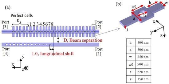
Figure 1.
(a) Geometry of the simulated uniform optical structure. Geometric parameters D (waveguide–cavity distance) and (mirror position) are shown. (b) Unit cell and geometric parameters of the unit cell in the perfect phoxonic crystal.
It is noted that the optical signal is injected and collected by means of waveport excitation, with radiation boundaries assumed elsewhere: the objective is to optimize the transfer of the optical excitation wave from the incident waveguide to the cavity. In Table 1 we report the values of the geometrical parameters of the cavity.

Table 1.
Uniform cavity parameters.
The efficiency of the coupling is based on the search of the maximum energy localized in the cavity, as a function of the parameters D and . In parallel, we need to keep low the transmission from the excited cavity towards both sides (ports 2 and 3 of Figure 1a) of the phoxonic cavity, to reduce losses. The following quantities have been calculated: optical quality factor, optical scattering parameters at the excitation ports, and opto-mechanical (OM) coupling, by using two different methods, to assess numerical consistency (first-order perturbation method and direct simulation by COMSOL multiphysics). Starting with a phoxonic crystal without the lateral waveguide, the field distributions of three optical eigenmodes with highest quality factors have been calculated and the results are reported in Figure 2.
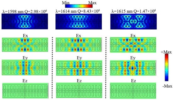
Figure 2.
Maps of the optical cavity modes for the uniform optomechanical (OM) cavity. Top pictures: E field magnitude, bottom pictures: real part of the E field components. Their imaginary parts are very small and not shown.
To illustrate the method for the optimization of the parameters D and , let us consider, for instance, the optical eigenmode located at the wavelength = 1615 nm, and chose = −50 nm. We expect that adding the lateral waveguide with Bragg mirror, and decreasing the distance D between the two waveguides, the values of the quality factor and the optical frequency of the photonic modes decrease owing to a higher coupling. The Bragg mirror is needed to maximize the electromagnetic (e.m.) transmission from the input waveguide to the cavity. Figure 3 shows the optical transmission/reflection and e.m. energy density curves obtained. Concerning the optical transmission, the source of the e.m. wave is located at port 1, as defined in Figure 1a, and the scattered waves are collected at all the four ports of the structure. With a unit input power, Figure 3a presents the transmission T through ports 2 or 3, the reflection R at port 1, as well as the radiated fraction of the power defined by 1-R-2T for different distance values D—between 500 and 700 nm—and assuming = −50 nm. Transmission at port 4 is almost zero. It can be noted that both the minimum reflection towards the input port 3 and the maximum of the radiated power are obtained for the same distance D around 550 nm. Figure 3b shows the highest e.m. energy density in the phoxonic crystal cavity, which also shows its maximum for the same distance D = 550 nm. This value of D defines the best coupling efficiency in terms of field strength in the cavity for the given value of . Now, the same operation needs to be repeated for different values of . Let us notice here that the phoxonic crystal must have a sufficient number of the perfect unit cells around the cavity in order to ensure a good confinement of the cavity mode and avoid leakage through ports 2 and 3.
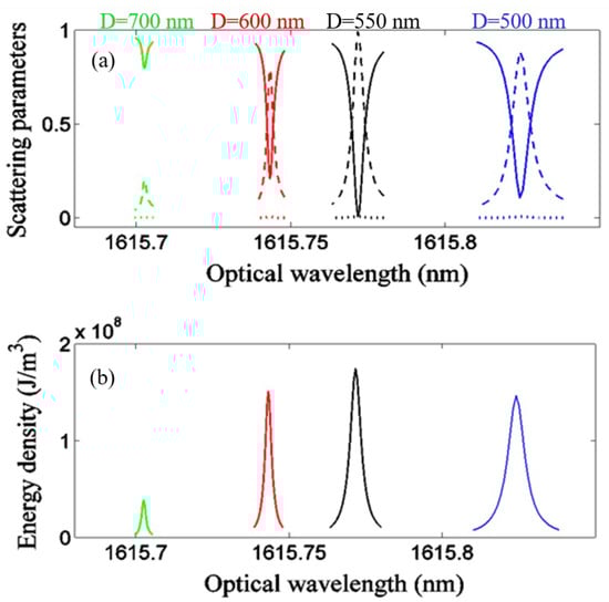
Figure 3.
Electromagnetic (e.m.) simulation of the cavity-waveguide system. (a) Transmission towards ports 2 or 3 (dotted lines), reflection towards port 1 (full lines) and radiated fraction of the optical power (dashed lines) for = 1615 nm in the geometry of Figure 1a. Transmission at port 4 is almost zero. (b) Energy density inside the cavity. The colors indicate the distance D between the phoxonic crystal and the optical waveguide while = −50 nm.
The remaining simulation steps involve the calculation of the OM coupling between the different detected photonic and phononic modes. It can be noted that the phoxonic structure has significant OM coupling rates between the three optical modes and two phononic ones located at Fphon = 2.39 GHz and Fphon = 2.43 GHz. In the calculation of the OM coupling, we have taken into account both mechanisms of photoelastic (PE) and moving interface (MI) effects, and get efficient OM coupling rates, gOM, ranging from 1 to 2 MHz. The mechanical displacement and the e.m. field distributions of these modes are shown in Figure 4. The mechanical motions correspond to a breathing of the stubs close to the cavity center. It should be noticed that despite their strong coupling rates, these two resonant mechanical modes fall outside the frequency range of the band gap around 2 GHz. In order to produce a downwards shift of these modes towards the gap, we design in the next section another cavity with a gradual variation of the stubs heights.
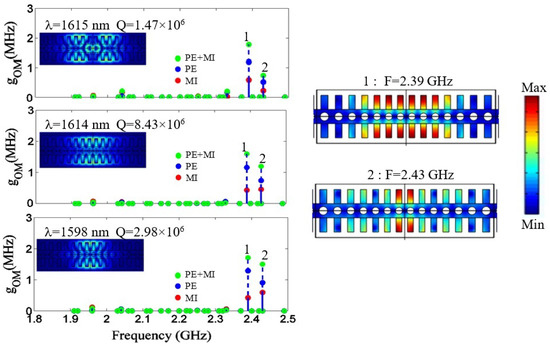
Figure 4.
Uniform cavity: optomechanical coupling with phonons around 2.4 GHz and maps of the phonon cavity modes. Both photoelastic (PE) and moving interface (MI) effects are considered.
2.2. Case of Study 2: Phoxonic Cavity with Parabolic Variations of the Stub Heights
A gradual variation of the stubs heights is needed in order not only to push the mechanical modes inside the phononic SS (symmetric–symmetric) band gap (see “Materials and Methods”), but also to improve the optical confinement and increase the resonant quality. In fact, the structured nanobeam cavity allows to get phononic modes working around 2.0 GHz and photonic ones at about 1.550 nm. We optimize the tapering rate over the lattice constants of the nanobeam and establish an excitation of the phononic/photonic cavity modes at the desired frequencies. The design of the tapered cavity has been done following a parabolic evolution of the elementary unit cell. Figure 5a shows the final design of the cavity. Figure 5b represents the unit cell of the perfect phoxonic crystal, and Table 2 reports the corresponding geometrical parameters. Assuming such parameters we obtained the excitation of 2 phononic modes closed to 2.0 GHz and 3 photonic modes closed to 1550 nm.
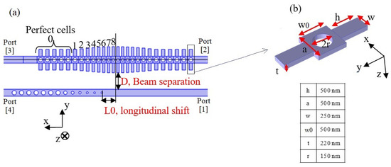
Figure 5.
(a) Geometry of the OM cavity with tapered stubs heights. (b) Unit cell and geometric parameters of the unit cell in the perfect phoxonic crystal.
Table 2.
Tapered cavity parameters.
Starting again with a phoxonic crystal without the lateral waveguide, for the case of parabolic tapering cavity, the field distributions of the three optical eigen modes with highest quality factors have been calculated: numerical results are reported in Figure 6. In comparison to the previous cavity, one can notice a similarity in the shape of the optical modes although their frequencies are shifted and the order of the modes has been changed.
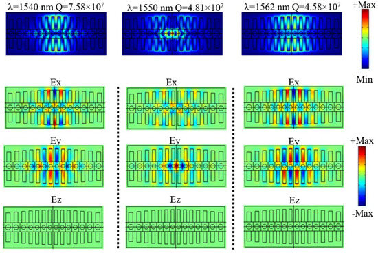
Figure 6.
Maps of the optical cavity modes for the tapered OM cavity. Top pictures: E field magnitude, bottom pictures: real part of the E field components. Their imaginary parts are very small and not shown.
Finally, the OM coupling rates between the three optical modes and the three phononic ones located at Fphon = 1.95, 2.002 and 2.05 GHz have been reported in Figure 7. The mechanical displacement and e.m. field distribution of the considered modes are shown in the same figure. The displacement fields mostly correspond to the motions of the stubs. Again, the coupling rates gOM range between 0.5 to 2 MHz.
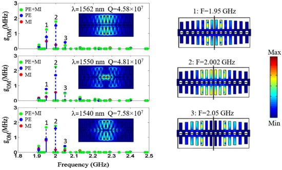
Figure 7.
Tapered cavity: optomechanical coupling with phonons around 2 GHz and maps of the phonon cavity modes. Both photoelastic (PE) and moving interface (MI) effects are considered.
3. Discussion
With reference to the optical scattering parameters and to the e.m. energy density in the cavities, we report a general view to the optical coupling calculations that was performed on the phoxonic crystal varying the geometric parameters D and . Figure 8 and Figure 9 show the results obtained for the uniform and tapered cavities, respectively. In order to estimate the best conditions for the optical coupling we need to take into account two main effects: the lower the distance D the better the coupling, but, consequently, the lower the quality factor Q of the cavity, due to optical leakeage from the cavity to the waveguide. In general, an optimum distance D can be found. As shown in Figure 8 and Figure 9, the optimum distance changes for different values of . For the uniform cavity, and for the considered resonant mode taken as an example ( nm), the best condition in terms of field strength in the cavity is given by = −50 nm, D = 550 nm; this allows us to achieve the highest e.m. energy density in the cavity and radiation power, and consequently the lowest reflection towards the input port, while maintaining a sufficiently high quality factor. Under these conditions, the energy density is 1.7 × 10 J/m, the quality factor is Q = 4 × 10, and the input reflection is about 0.0062.
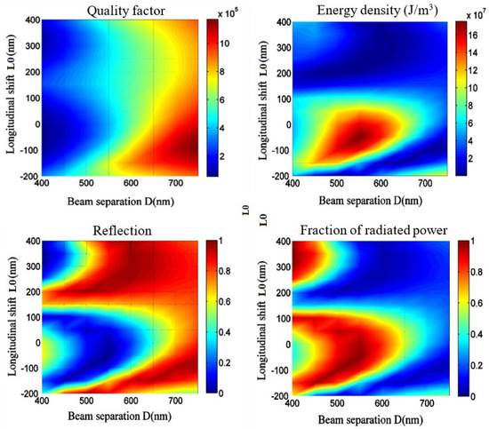
Figure 8.
Optimization of D and for the optical mode at = 1615 nm (uniform cavity).
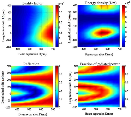
Figure 9.
Optimization of D and for the optical mode at = 1550 nm (tapered cavity).
For the case of cavity with parabolic tapering of the stub heigths, the optimum conditions for D and have been also estimated as follows. For the considered resonant mode taken as an example ( nm), the best condition in terms of field strength in the cavity is given by = 0 nm, D = 550 nm. In this case, the resulting energy density is 8 × 10 J/m, the input reflection is 0.0067, and the quality factor is Q = 1.71 × 10.
The numerical results just obtained for uniform and parabolic OM cavities have been compared in Figure 10. From this figure, one can note that the optimal parameters D and are different from one mode to another, Indeed, for the mode located at 1615 nm (resp. 1550 nm for the parabolic cavity) the optimal parameters are D = 550 nm and = −50 nm (resp. D = 550 nm and = 0), whereas the optimal optical coupling of the mode located at 1598 nm (resp. 1540 nm for the parabolic cavity) is obtained for relatively greater distances of D = 650 nm and = 250 nm (resp. D = 700 nm and = 250 nm). This difference can be explained from the spatial distribution of the electric field associated with each mode. Indeed, the electric field associated with the second mode penetrates more into the stubs and becomes closer to the waveguide transporting the incident field. By exploiting the additional degree of freedom given by the modulation of stub heights, we have achieved better quality factors and higher energy densities of the e.m. field excited in the cavities by the lateral waveguide.
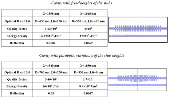
Figure 10.
Optical features of uniform and tapered cavities: comparison of numerical results.
4. Materials and Methods
In this section, we provide detailed definition of the phoxonic crystal and simulation setup used in numerical calculation. All simulations have been performed using finite element methods implemented by COMSOL multiphysics solver. The typical geometry under consideration, and related simulation setup, is shown in Figure 11. Two suspended Si nanobeams are used to confine the optical signal at infrared frequency, and to host respectively a resonant OM cavity and a Bragg mirror. We varied the distance between the two nanoguides D and the position of the Bragg mirror with respect to the middle of the cavity to maximize their coupling. It is noted in Figure 11 that the optical signal is injected and collected by means of wave-port excitation, with radiation boundaries, or alternatively perfect matched layers, assumed elsewhere.
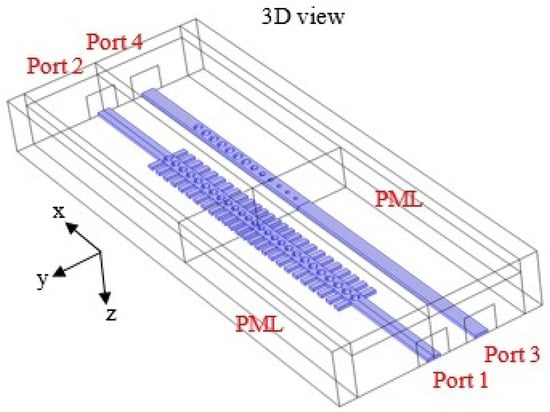
Figure 11.
Modelling setup: simulated optical structure.
A frequency dispersion characterization of the periodic cells was needed to obtain both optical and mechanical resonant modes in pre-defined bands. In order to increase the mechanical quality factor of OM cavities patterned in nanobeams, several strategies have been recently used [34], such as, for instance, uniform stress, soft-clamping, and geometric strain engineering. In the present work, we acted on stubs size and distribution across the beam length to modulate the resonant wavelength of the mechanical modes: specifically, increasing stub length and width usually produces an increase of the resonant wavelength. In this way, we place the mode resonances in the mechanical band gap of the periodic part of the cavity crystal, so that the quality factor is maximized. As mentioned above, the geometrical parameters of the phoxonic nanobeam are designed to obtain the optical resonances around 1550 nm and the acoustic resonances around 2 GHz. The latter is also a suitable choice to make easier an independent excitation of the acoustic cavity modes by means of SAW generated by interdigitated electrodes on a multilayer substrate in front of the nanobeam as shown in our recent work [23]. We show in Figure 12 the dispersion curves for the mechanical (Figure 12a) and optical (Figure 12b) modes, related to the unit cell of Figure 1b. The different branches are characterized according to their symmetry (S (symmetric) or A (anti-symmetric)) with respect to the two symmetry planes xOz and xOy of the structure. Only symmetric modes with respect to the xOy plane are presented whereas the red and blue colors refer to the S and A modes with respect to the xOz plane. It should be stressed that, based on symmetry consideration, only mechanical modes of SS symmetry can display an efficient OM coupling [10,11,32] as studied in the previous sections. In Figure 12, one can notice a full photonic band gap below the light line of vacuum, represented by the gray shaded area. On the other hand, a band gap of SS symmetry is obtained for acoustic modes around 2 GHz. The optical and elastic properties used in the calculation are provided in Table 3, where Cij are the elastic constants, Pij are the photo-elastic coefficients, is the mass density, and n is the refractive index.
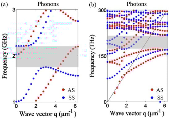
Figure 12.
(a) Phononic and (b) photonic dispersion curves. The red and blue branches respectively correspond to the Anti-symmetric (A) and Symmetric (S) modes with respect to the xOz plane. All the considered branches are Symmetric (S) with respect to the xOy plane. The shaded area corresponds to the bandgaps. The straight line in panel (b) is the light line in vacuum.
Table 3.
Optical, elastic and photoelastic properties of silicon.
It is remarked that all simulations related to the complete structure (Figure 11) have been performed with particular care to possible numerical issues, which are strongly amplified by the high Q resonance of the considered cavities:
- -
- spatial mesh: changing any geometrical parameter means changing the mesh, then the numerical impact of changing the mesh must be minimized;
- -
- radiating boundaries: even a small reflection from the radiating boundary could strongly impact the final results due the high Q of the cavity, so PML thickness and distance can become critical parameters. In order to overcome this issue, several tests have been made varying PML thickness and position, until consistent and repeatable results were obtained;
- -
- e.m. excitation waveports: port size could be too small to correctly capture the slab guided mode, but ports cannot be made too large otherwise (i) they overlap when reducing D and (ii) they indesirably intercept radiated field. In general a good compromize for the port size is needed, and, anyway, other approaches are possible: the computational domain can be extended to allow proper calibration of the electromagnetic field excitation coming from the waveports.
5. Conclusions
In this work, we investigated the optomechanical interaction taking place in a corrugated phoxonic silicon nanobeam where periodic loads (stubs) and holes are designed to provide simultaneous bandgaps for photonic and phononic modes, and where an integrated waveguided is used to effectively excite mode resonances. Such a choice prevents from the need of an external fiber excitation, and contributes to the possibility of component integration, scalability, and circuit compactness. With respect to the state of the art of OM cavities, we have introduced an additional parabolic taper of the periodic stubs of the involved photonic crystal, in order to: (i) place the mechanical mode resonances in the mechanical band gap of the periodic crystal of the cavity, (ii) optimize the distance between the cavity and the integrated waveguided, and the position of the Bragg mirror patterned in the lateral waveguide, to allow maximum e.m. field transfer to the cavity, (iii) ensure a proper spacing between the lateral integrated waveguide and the cavity out of the coupling region, (iv) maximize phononic and photonic modes confinement with high quality factors, in order to enhance their OM interaction. Comparison of the results obtained in the case of a cavity with uniform heights of the stubs has been also reported. Concerning the OM coupling coefficients, high coupling rates were found, up to 2 MHz, with photonic quality factor up to for the parabolic cavity. Symmetry of the acoustic modes was considered in order to select only those that could couple with the confined photonic modes. Both moving interface and photoelastic contributions are included in the calculation of OM couplings. Finally, the numerical features of the performed simulations have been discussed to ensure repeatability of the analysis.
Author Contributions
Conceptualization, all Authors; methodology, all Authors; software, A.G., D.M.; validation, A.G., D.M.; formal analysis, all Authors; investigation, all Authors; resources, all authors; data curation, all authors; writing–original draft preparation, D.M.; writing–review and editing, all authors; visualization, all Authors; supervision, all Authors; project administration, D.M., Y.P., B.D.R., and L.P.; funding acquisition, D.M., Y.P., B.D.R., and L.P. All authors have read and agreed to the published version of the manuscript.
Funding
This research was funded by the European Project entitled “All-Phononic circuits Enabled by Opto-mechanics” (PHENOMEN), H2020 FETOPEN 2014-2015-RIA, n.713450.
Conflicts of Interest
The authors declare no conflict of interest.
Abbreviations
The following abbreviations are used in this manuscript:
| OM | Opto-mechanical |
| AO | Acousto-Optic |
| PE | Photo-elastic |
| e.m. | electromagnetic |
| MI | Moving Interface |
| SS | Symmetric–Symmetric |
References
- Aspelmeyer, M.; Kippenberg, T.; Marquardt, F. Cavity optomechanics. Rev. Mod. Phys. 2014, 86, 1391–1452. [Google Scholar] [CrossRef]
- Kippenberg, T.; Vahala, K. Cavity optomechanics: Back-action at the mesoscale. Science 2008, 321, 1172–1176. [Google Scholar] [CrossRef] [PubMed]
- Favero, I.; Karrai, K. Optomechanics of deformable optical cavities. Nat. Photonics 2009, 3, 201–205. [Google Scholar] [CrossRef]
- Eichenfield, M.; Chan, J.; Camacho, R.; Vahala, K.; Painter, O. Optomechanical crystals. Nature 2009, 462, 78–82. [Google Scholar] [CrossRef] [PubMed]
- Gavartin, E.; Braive, R.; Sagnes, I.; Arcizet, O.; Beveratos, A.; Kippenberg, T.; Robert-Philip, I. Optomechanical coupling in a two-dimensional photonic crystal defect cavity. Phys. Rev. Lett. 2011, 106, 203902. [Google Scholar] [CrossRef] [PubMed]
- Fuhrmann, D.; Thon, S.; Kim, H.; Bouwmeester, D.; Petroff, P.; Wixforth, A.; Krenner, H. Dynamic modulation of photonic crystal nanocavities using gigahertz acoustic phonons. Nat. Photonics 2011, 5, 605–609. [Google Scholar] [CrossRef]
- Chan, J.; Safavi-Naeini, A.; Hill, J.; Meenehan, S.; Painter, O. Optimized optomechanical crystal cavity with acoustic radiation shield. Appl. Phys. Lett. 2012, 101, 081115. [Google Scholar] [CrossRef]
- Rolland, Q.; Oudich, M.; El-Jallal, S.; Dupont, S.; Pennec, Y.; Gazalet, J.; Kastelik, J.; Lévêque, G.; Djafari-Rouhani, B. Acousto-optic couplings in two-dimensional phoxonic crystal cavities. Appl. Phys. Lett. 2012, 101, 061109. [Google Scholar] [CrossRef]
- Djafari-Rouhani, B.; El-Jallal, S.; Pennec, Y. Phoxonic crystals and cavity optomechanics [Cristaux phoxoniques et optomécaniques dans les cavités]. C. R. Phys. 2016, 17, 555–564. [Google Scholar] [CrossRef]
- Oudich, M.; El-Jallal, S.; Pennec, Y.; Djafari-Rouhani, B.; Gomis-Bresco, J.; Navarro-Urrios, D.; Sotomayor Torres, C.M.; Martínez, A.; Makhoute, A. Optomechanic interaction in a corrugated phoxonic nanobeam cavity. Phys. Rev. B 2014, 89, 245122. [Google Scholar] [CrossRef]
- Gomis-Bresco, J.; Navarro-Urrios, D.; Oudich, M.; El-Jallal, S.; Griol, A.; Puerto, D.; Chavez, E.; Pennec, Y.; Djafari-Rouhani, B.; Alzina, F.; et al. A one-dimensional optomechanical crystal with a complete phononic band gap. Nat. Commun. 2014, 5, 4452. [Google Scholar] [CrossRef] [PubMed]
- Maire, J.; Arregui, G.; Capuj, N.; Colombano, M.; Griol, A.; Martinez, A.; Sotomayor-Torres, C.; Navarro-Urrios, D. Optical modulation of coherent phonon emission in optomechanical cavities. APL Photonics 2018, 3, 126102. [Google Scholar] [CrossRef]
- Mohammade, S.; Eftekhar, A.; Khelif, A.; Adibi, A. Simultaneous two-dimensional phononic and photonic band gaps in opto-mechanical crystal slabs. Opt. Express 2010, 18, 9164–9172. [Google Scholar] [CrossRef] [PubMed]
- Pennec, Y.; Djafari Rouhani, B.; El Boudouti, E.; Li, C.; El Hassouani, Y.; Vasseur, J.; Papanikolaou, N.; Benchabane, S.; Laude, V.; Martinez, A. Simultaneous existence of phononic and photonic band gaps in periodic crystal slabs. Opt. Express 2010, 18, 14301–14310. [Google Scholar] [CrossRef]
- Maldovan, M. Sound and heat revolutions in phononics. Nature 2013, 503, 209–217. [Google Scholar] [CrossRef]
- Arcizet, O.; Cohadon, P.F.; Briant, T.; Pinard, M.; Heidmann, A. Radiation-pressure cooling and optomechanical instability of a micromirror. Nature 2006, 444, 71–74. [Google Scholar] [CrossRef]
- Gigan, S.; Böhm, H.; Paternostro, M.; Blaser, F.; Langer, G.; Hertzberg, J.; Schwab, K.; Bäuerle, D.; Aspelmeyer, M.; Zeilinger, A. Self-cooling of a micromirror by radiation pressure. Nature 2006, 444, 67–70. [Google Scholar] [CrossRef]
- Aspelmeyer, M.; Meystre, P.; Schwab, K. Quantum optomechanics. Phys. Today 2012, 65, 29–35. [Google Scholar] [CrossRef]
- Balram, K.; Davanço, M.; Song, J.; Srinivasan, K. Coherent coupling between radiofrequency, optical and acoustic waves in piezo-optomechanical circuits. Nat. Photonics 2016, 10, 346–352. [Google Scholar] [CrossRef]
- Vainsencher, A.; Satzinger, K.; Peairs, G.; Cleland, A. Bi-directional conversion between microwave and optical frequencies in a piezoelectric optomechanical device. Appl. Phys. Lett. 2016, 109, 033107. [Google Scholar] [CrossRef]
- Balram, K.; Davanço, M.; Ilic, B.; Kyhm, J.H.; Song, J.; Srinivasan, K. Acousto-Optic Modulation and Optoacoustic Gating in Piezo-Optomechanical Circuits. Phys. Rev. Appl. 2017, 7, 024008. [Google Scholar] [CrossRef] [PubMed]
- Munk, D.; Katzman, M.; Hen, M.; Priel, M.; Feldberg, M.; Sharabani, T.; Levy, S.; Bergman, A.; Zadok, A. Surface acoustic wave photonic devices in silicon on insulator. Nat. Commun. 2019, 10, 4214. [Google Scholar] [CrossRef] [PubMed]
- Korovin, A.; Pennec, Y.; Stocchi, M.; Mencarelli, D.; Pierantoni, L.; Makkonen, T.; Ahopelto, J.; Djafari Rouhani, B. Conversion between surface acoustic waves and guided modes of a quasi-periodic structured nanobeam. J. Phys. D Appl. Phys. 2019, 52, 32. [Google Scholar] [CrossRef]
- Forsch, M.; Stockill, R.; Wallucks, A.; Marinković, I.; Gärtner, C.; Norte, R.; van Otten, F.; Fiore, A.; Srinivasan, K.; Gröblacher, S. Microwave-to-optics conversion using a mechanical oscillator in its quantum ground state. Nat. Phys. 2020, 16, 69–74. [Google Scholar] [CrossRef]
- Yu, W.; Jiang, W.; Lin, Q.; Lu, T. Cavity optomechanical spring sensing of single molecules. Nat. Commun. 2016, 7, 12311. [Google Scholar] [CrossRef]
- Delić, U.; Reisenbauer, M.; Dare, K.; Grass, D.; Vuletić, V.; Kiesel, N.; Aspelmeyer, M. Cooling of a levitated nanoparticle to the motional quantum ground state. Science 2020, 367, 892–895. [Google Scholar] [CrossRef]
- Djorwe, P.; Pennec, Y.; Djafari-Rouhani, B. Exceptional Point Enhances Sensitivity of Optomechanical Mass Sensors. Phys. Rev. Appl. 2019, 12, 024002. [Google Scholar] [CrossRef]
- Fang, K.; Matheny, M.; Luan, X.; Painter, O. Optical transduction and routing of microwave phonons in cavity-optomechanical circuits. Nat. Photonics 2016, 10, 489–496. [Google Scholar] [CrossRef]
- Colombano, M.F.; Arregui, G.; Capuj, N.E.; Pitanti, A.; Maire, J.; Griol, A.; Garrido, B.; Martinez, A.; Sotomayor-Torres, C.M.; Navarro-Urrios, D. Synchronization of Optomechanical Nanobeams by Mechanical Interaction. Phys. Rev. Lett. 2019, 123, 017402. [Google Scholar] [CrossRef]
- Gil-Santos, E.; Labousse, M.; Baker, C.; Goetschy, A.; Hease, W.; Gomez, C.; Lemaître, A.; Leo, G.; Ciuti, C.; Favero, I. Light-Mediated Cascaded Locking of Multiple Nano-Optomechanical Oscillators. Phys. Rev. Lett. 2017, 118, 063605. [Google Scholar] [CrossRef]
- Stockill, R.; Forsch, M.; Beaudoin, G.; Pantzas, K.; Sagnes, I.; Braive, R.; Gröblacher, S. Gallium Phosphide as a Piezoelectric Platform for Quantum Optomechanics. Phys. Rev. Lett. 2019, 123, 163602. [Google Scholar] [CrossRef]
- Stocchi, M.; Mencarelli, D.; Pennec, Y.; Djafari-Rouhani, B.; Pierantoni, L. Rigorous simulation of nonlinear optomechanical coupling in micro-and nano-structured resonant cavities. Int. J. Optomechatron. 2018, 12, 11–19. [Google Scholar] [CrossRef]
- Mencarelli, D.; Stocchi, M.; Pierantoni, L. Electromagnetic amplification of microwave phonons in nonlinear resonant microcavities. IEEE Trans. Microw. Theory Tech. 2018, 66, 3603–3610. [Google Scholar] [CrossRef]
- Ghadimi, A.H.; Fedorov, S.A.; Engelsen, N.J.; Bereyhi, M.J.; Schilling, R.; Wilson, D.J.; Kippenberg, T.J. Elastic strain engineering for ultralow mechanical dissipation. Science 2018, 360, 764–768. [Google Scholar] [CrossRef] [PubMed]


© 2020 by the authors. Licensee MDPI, Basel, Switzerland. This article is an open access article distributed under the terms and conditions of the Creative Commons Attribution (CC BY) license (http://creativecommons.org/licenses/by/4.0/).