Article

Collective Lattice Resonances in All-Dielectric Nanostructures under Oblique Incidence

by
Anton D. Utyushev
1,2,3,
Vadim I. Zakomirnyi
1,3,
Alexander E. Ershov
1,2,3,
Valeriy S. Gerasimov
1,3,
Sergey V. Karpov
1,2,4 and
Ilia L. Rasskazov
5,*
1
Department of Engineering Physics and Radioelectronics, Siberian Federal University, 660041 Krasnoyarsk, Russia
2
Department of Space Materials and Technology, Siberian State University of Science and Technology, 660014 Krasnoyarsk, Russia
3
Institute of Computational Modeling SB RAS, 660036 Krasnoyarsk, Russia
4
L. V. Kirensky Institute of Physics, Federal Research Center KSC SB RAS, 660036 Krasnoyarsk, Russia
5
The Institute of Optics, University of Rochester, Rochester, NY 14627, USA
*
Author to whom correspondence should be addressed.
Photonics 2020, 7(2), 24; https://doi.org/10.3390/photonics7020024
Submission received: 28 February 2020 / Revised: 24 March 2020 / Accepted: 25 March 2020 / Published: 28 March 2020
(This article belongs to the Special Issue Optical Nanoantennas)

Abstract

:
Collective lattice resonances (CLRs) emerging under oblique incidence in 2D finite-size arrays of Si nanospheres have been studied with the coupled dipole model. We show that hybridization between the Mie resonances localized on a single nanoparticle and angle-dependent grating Wood–Rayleigh anomalies allows for the efficient tuning of CLRs across the visible spectrum. Complex nature of CLRs in arrays of dielectric particles with both electric dipole (ED) and magnetic dipole (MD) resonances paves a way for a selective and flexible tuning of either ED or MD CLR by an appropriate variation of the angle of incidence. The importance of the finite-size effects, which are especially pronounced for CLRs emerging for high diffraction orders under an oblique incidence has been also discussed.

1. Introduction

All-dielectric nanophotonics, being a rapidly emerging field of modern physics [1], provides a low-loss platform for an impressive number of applications. Well-developed state-of-the-art methods for synthesis of different all-dielectric materials [2] enable their successful implementation in color printing [3,4,5,6,7], biosensing [8,9,10], lasing [11,12], waveguiding [13,14,15], optical filtering [16,17,18], and nonlinear [19,20,21,22,23] optics. Among a rich variety of electromagnetic phenomena arising in all-dielectric nanostructures, collective effects in regular arrays of nanoparticles (NPs) have attracted a lot of attention recently [24,25,26,27,28,29,30,31,32,33,34,35,36,37], which is justified by the appearance of non-trivial lattice-mediated phenomena—for example, suppression of the back-scattering (Kerker effect) [38,39,40,41].
Collective lattice resonances (CLRs) arising in arrays of NPs originate from the strong interaction between NPs composing the lattice, which usually occurs under the illumination with a wavelength close to Wood–Rayleigh anomalies (WRAs) [42,43] of the array. In this case, a majority of NPs are excited with the same phase, which results in ultra-narrow high-Q spectral features. CLRs have been well studied for nanostructures from plasmonic NPs for a long time [44,45,46,47,48,49,50,51,52,53,54,55,56], while the all-dielectric analogues have gained attention only a decade ago [57]. In contrast to plasmonic NPs (in most of the cases characterized by weak magnetic and strong electric responses), all-dielectric NPs with pronounced electric and magnetic optical resonances [58] give rise to a rich variety of tunable CLRs that emerge even in regular rectangular-shaped arrays [32]. Moreover, 2D structures from all-dielectric NPs with two distinct electric dipole (ED) and magnetic dipole (MD) resonances exhibit inherently more sophisticated and intriguing behavior compared to the respective situations in purely ED-responsive plasmonic arrays, for example, in disordered [36,59] and finite-size [37,38,60,61,62] lattices.
Most of the numerical and theoretical studies of CLRs deal with infinitely large arrays of NPs under a normal incidence; however, it can be easily anticipated that, under oblique incidence, all-dielectric arrays may exhibit a plethora of properties overlooked in the literature. Our expectations are well justified by the reported results for plasmonic arrays [63,64] (with only ED response), which imply that, for all-dielectric NPs with ED and MD resonances, one may expect to observe even more effects. Thus, in this work, we address this problem and study electromagnetic properties of 2D arrays of all-dielectric NPs under oblique illumination. Moreover, we focus on finite-size arrays and reveal a role of the array size (in terms of a total number of NPs composing the lattice) on CLRs emerged under such conditions, which is more relevant to the experimental setups than infinite-array approximation.

2. Model

2.1. Coupled Dipole Approximation

Consider an array from N tot spherical NPs embedded in a vacuum and illuminated by a plane wave, which, at any location r , reads as
E inc ( r ) = E 0 exp ( i k · r ) , H inc ( r ) = H 0 exp ( i k · r ) ,
where E 0 = E 0 x , E 0 y , E 0 z and H 0 = H 0 x , H 0 y , H 0 z are amplitudes of the electric and magnetic fields, and k is a wave vector. The time dependence exp ( i ω t ) is assumed and suppressed throughout a paper. In the framework of point-dipole approximation, electric, d i , and magnetic, m i , dipole moments induced on a given i-th NP under such an incidence are coupled to the respective dipoles on other j i NPs and to the external field as [57,65,66] (unlike these works, we use Gauss units)
d i = α e E inc ( r i ) + j i N tot G i j d j j i N tot C i j m j , m i = α m H inc ( r i ) + j i N tot G i j m j + j i N tot C i j d j ,
where r i is the position of the i-th NP center, α e = 3 i a 1 / 2 k 3 and α m = 3 i b 1 / 2 k 3 are electric and magnetic dipole polarizabilities, where a 1 and b 1 are scattering coefficients [67], k = | k | = 2 π / λ , and λ is a wavelength. Tensors G i j and C i j describe the interaction between dipoles induced on i-th and j-th NPs:
G i j = exp ( i k r i j ) r i j k 2 1 r i j 2 + i k r i j I + k 2 + 3 r i j 2 3 i k r i j r i j r i j r i j 2 ,
C i j α β = γ ε α γ β ( g i j ) γ , g i j = exp ( i k r i j ) r i j k 2 + i k r i j r i j r i j ,
where I is a 3 × 3 unit tensor, ⊗ denotes a tensor product, r i j = | r i j | = | r i r j | is center-to-center distance between i-th and j-th NPs, and ε α γ β is Levi–Civita symbol with α , β , γ denoting Cartesian components of the tensors.
For an array with a given geometry and composition of NPs, the solution of the linear system of Equations (1) yields d i and m i induced on each i-th NP; thus, the electromagnetic response of the array to the incident excitation can be explicitly found. Particularly, in this work, we consider the total amount of the electromagnetic energy scattered and absorbed by the array normalized to the sum of the cross sectional area of all NPs, i.e., the extinction efficiency [57,66]:
Q ext = 4 k | E 0 | 2 N tot R 2 i = 1 N tot d i · E inc ( r i ) + m i · H inc ( r i ) ,
where the asterisk denotes a complex conjugate, R is the radius of the NP, and ℑ takes the imaginary part.

2.2. Wood–Rayleigh Anomalies
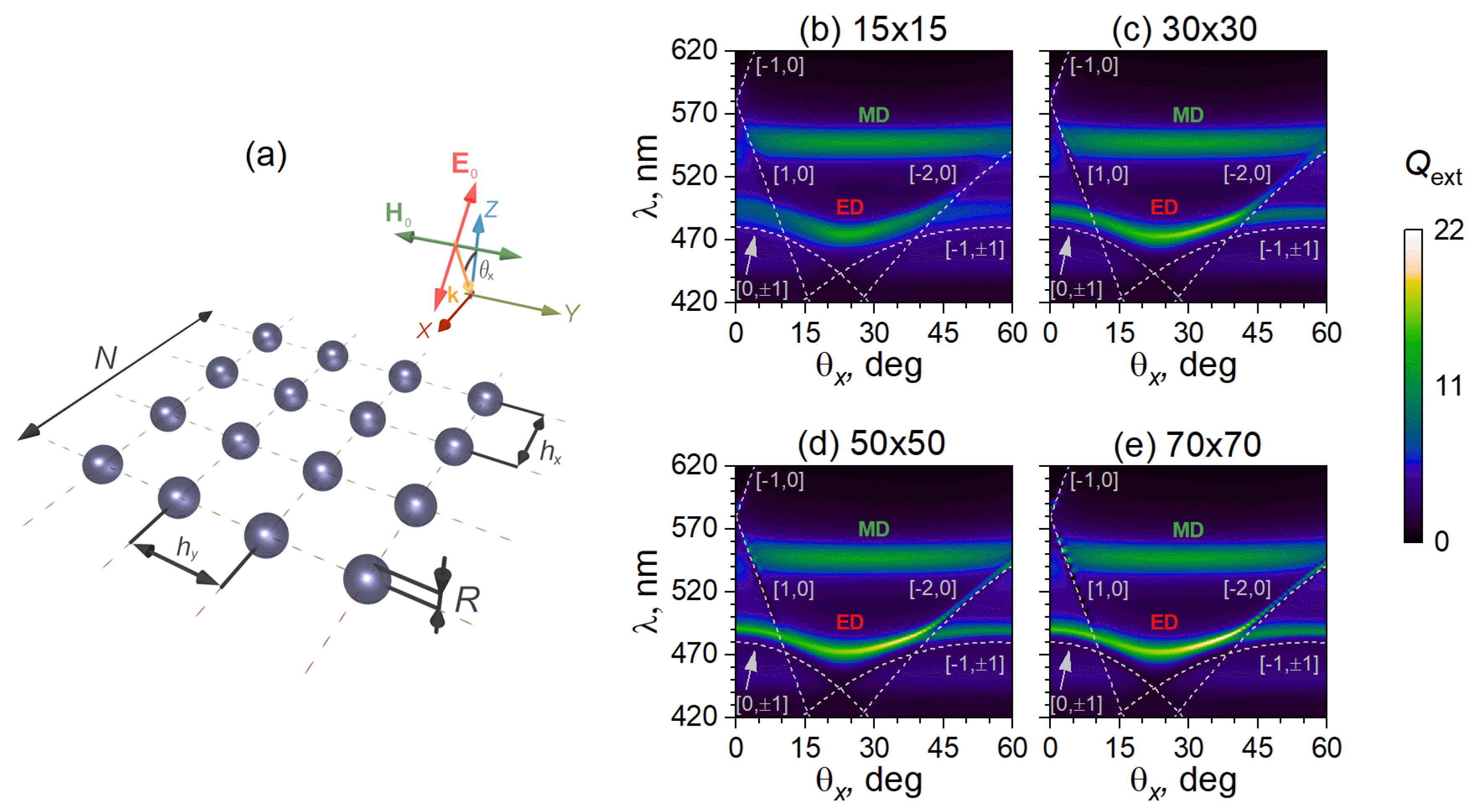
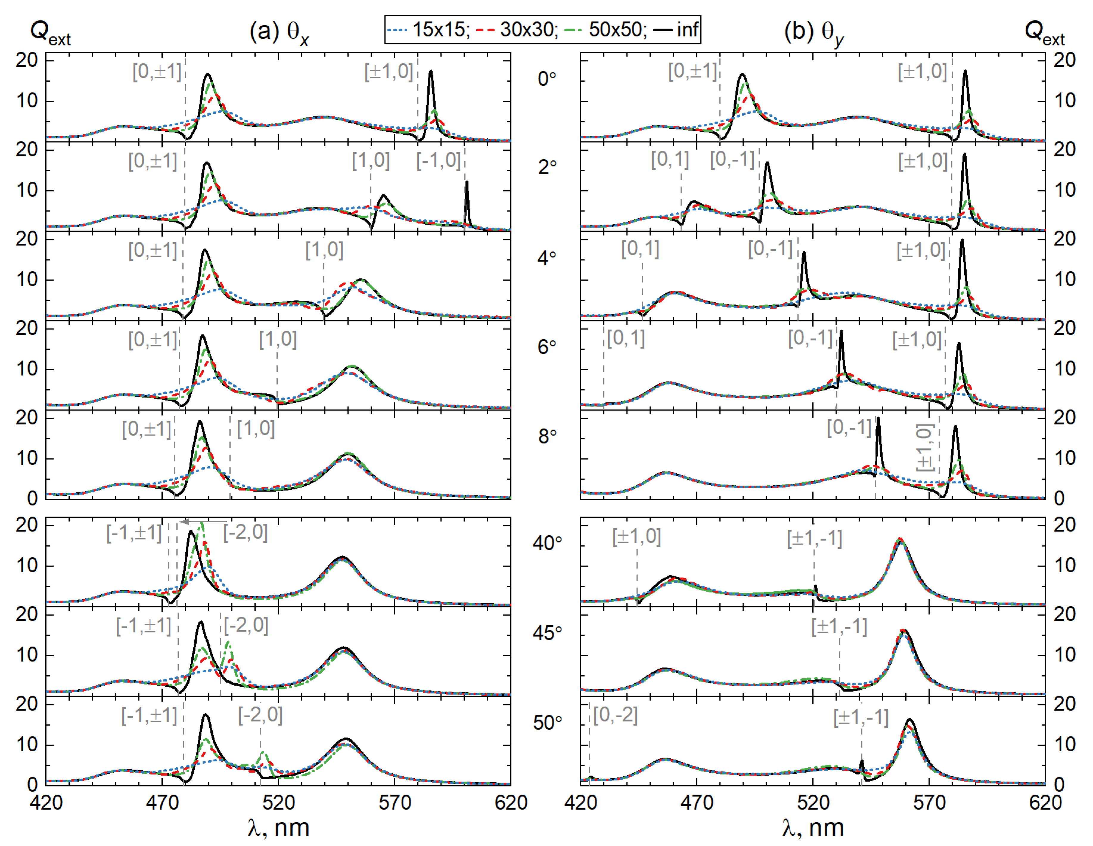
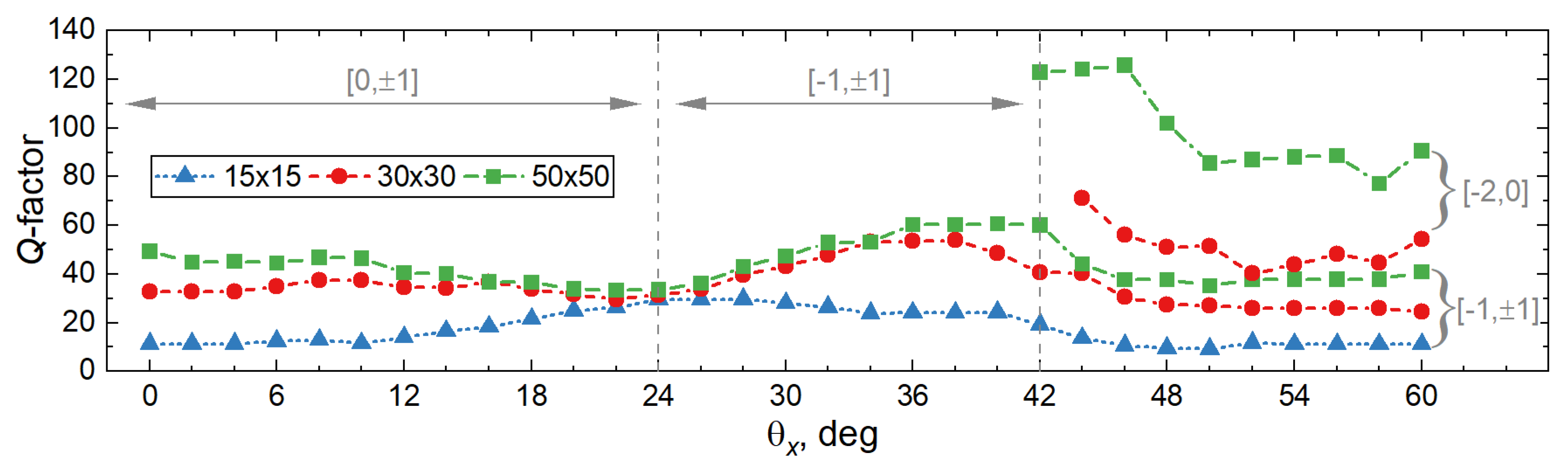
CLRs emerge at wavelengths close (slightly red-shifted) to WRAs, which for a general case of a regular 2D lattice (with pitches h x and h y along x and y axes, as shown in Figure 1a) takes place if
k = k σ + p K x + q K y ,
where K x = ( 2 π / h x ) x ^ and K y = ( 2 π / h y ) y ^ are reciprocal lattice vectors, k = ( k x , k y ) is wave vector of a wave propagating in the lattice plane, k σ is projection of the incident wave vector on the lattice plane, [ p , q ] is a pair of integers which denotes the order of the anomaly, and symbol ^ denotes a unit vector. Explicitly, x and y components in Equation (3) read as
k x = 2 π λ sin θ x + 2 π h x p , k y = 2 π λ sin θ y + 2 π h y q ,
where θ x and θ y are angles between the z-axis and projections of k to X O Z and Y O Z planes (see Figure 1a and Figure 2a, respectively).
In a homogeneous environment, the wave vector of a wave propagating in the lattice plane is | k | 2 = k x 2 + k y 2 = ( 2 π / λ ) 2 , which along with Equation (4) provide the quadratic equation in λ :
p 2 h x 2 + q 2 h y 2 λ 2 + 2 p sin θ x h x + q sin θ y h y λ + sin 2 θ x + sin 2 θ y 1 = 0 ,
where, for a given combination of integers [ p , q ] , one can get a corresponding spectral position λ p , q of WRA of [ p , q ] order.
We emphasize that the hybridization between localized Mie resonances and [ ± 1 , 0 ] or [ 0 , ± 1 ] WRAs is usually considered in a solid body of the literature [32,36,37,57]. For a special case of normal incidence ( θ x = θ y = 0 ), these WRAs are simply λ ± 1 , 0 = h x and λ 0 , ± 1 = h y . However, Equation (5) immediately implies that the broad variation of θ x and/or θ y may result in CLRs emerging from the hybridization with WRAs of higher order (i.e., | p | , | q | > 1 ), which are studied below.

3. Results

We consider regular arrays from Si NPs with R = 65 nm, arranged in a 2D rectangular lattice with h y = 480 nm and h x = 580 nm. A direct comparison with full-field simulations ([31] Figure 1) ([38] Figure 3) has confirmed a reliability of the coupled dipole approximation (1) for arrays with similar pitches and the same R. Under a normal incidence with E 0 = E 0 x , 0 , 0 and H 0 = 0 , H 0 y , 0 , arrays with these geometrical parameters exhibit ED and MD CLRs ([37] Figure 2b) at λ 490 nm and λ 586 nm, respectively, which is the result of a hybridization between ED ( λ 450 nm) and MD ( λ 550 nm) resonances of a single NP ([57] Figure 3b) with [ 0 , ± 1 ] and [ ± 1 , 0 ] WRAs ([37] Figure 2a), correspondingly. Since the efficient tuning of ED and MD CLRs occurs if h y , x are changed in a direction perpendicular with respect to the polarization of E 0 or H 0 ([32] Figures 2 and 4), ([36] Figure 2), it is insightful to consider an incidence with only one θ x , y varied keeping the other θ y , x = 0 . Following this approach, it is possible to study separately ED and MD CLRs, while, for any other oblique incidence with θ x 0 and θ y 0 , one can expect the optical response to be a superposition of the studied examples.
Figure 1b–e show the extinction efficiency for arrays with different N tot = N × N under incidence with 0 θ x 60 and θ y = 0 . Dashed [ p , q ] lines show corresponding angle-dependent λ p , q for WRA which fall within a visible range for a geometry considered. It can be seen that, apart from common [ 0 , ± 1 ] and [ ± 1 , 0 ] , WRAs of [ 2 , 0 ] and [ 1 , ± 1 ] orders have emerged. This leads to the appearance of additional ED CLRs for [ 1 , ± 1 ] WRA under θ x > 25 illumination, and for [ 2 , 0 ] WRA under θ x > 40 incidence. Moreover, even for θ y = 0 , variation of θ x implies gradual blue-shift of [ 0 , ± 1 ] WRA, which allows for fine-tuning of ED CLRs for θ x < 25 . Such angle-dependent hybridization between Mie resonances on single NP and WRAs paves a way for the efficient tuning of ED CLRs in the 450–540 nm range. It is noteworthy that MD CLR vanishes quite rapidly with a slight change of θ x , since λ ± 1 , 0 strongly depends on θ x (cf. Equation (5)); thus, for θ x > 5 , only an MD resonance of a single NP is observed. As it might be expected from Ref. [37], the extinction efficiency at the CLR regime grows with N tot ; thus, the CLRs that have emerged from the interaction with high-order WRAs are more pronounced for larger arrays, which can be clearly seen by the following Figure 1b for the array from 15 × 15 NPs to Figure 1e for 70 × 70 NPs.
On the contrary, by changing θ y and keeping θ x = 0 constant, one can control the spectral position of MD CLRs, as clearly shown in Figure 2. In this case, however, ED CLR does not vanish so rapidly for 0 < θ y < 5 (as it does MD CLR from Figure 1 for the opposite case of 0 < θ x < 5 ). ED resonance on a single NP efficiently couples to [ 0 , 1 ] WRA and thus corresponding ED CLR can be tuned all the way up to 570 nm, and, finally, overlap with [ ± 1 , 0 ] MD CLR around 580 nm under θ y 12 incidence. MD CLR, however, can be efficiently tuned only for [ ± 1 , 0 ] WRA, while, wavelengths of high-order WRAs appear to be quite far away from MD resonance, and only [ ± 1 , 1 ] efficiently interacts with MD resonance, but for quite large angles of incidence.
Figure 3 further elaborates on discussed effects and shows several extinction spectra for the clearer presentation. Indeed, under oblique incidence, one can observe efficient tuning of the optical properties of the 2D lattice from Si NPs. The “gradual” quadratic λ p , q ( θ 2 ) and “rapid” linear λ p , q ( θ ) dependence with one of the θ x , y being zero (see Equation (5)) allows for a flexible control of ED and MD CLRs. For a strong coupling of single-particle resonance with WRAs (i.e., for spectral regions where they almost overlap), the finite size effects are of particular importance, while, for a weakly coupled case (i.e., for spectral regions where they are sufficiently far from each other), these effects have a minor impact. For example, from Figure 3a, one can see that Q ext rapidly grows with increasing N × N for ED CLR strongly coupled to [ 0 , ± 1 ] around λ 490 nm, while MD CLR for [ 1 , 0 ] WRA becomes almost independent on N tot with increasing θ x .
Finally, Figure 4 demonstrates angle-dependent Q-factors of ED CLRs from Figure 1, for arrays with different N × N . As it might be expected, the Q-factor is generally larger for arrays with larger N × N . Interestingly, for 0 θ x 24 incidence, with increasing θ x , i.e., weakening coupling between single-particle resonance and [ 0 , ± 1 ] WRA, Q-factor gradually converges to 30 value for any array size at θ x 24 . It is noteworthy that for CLRs that have emerged from the hybridization with high-order [ 2 , 0 ] WRA, Q-factor is about two times larger than that of commonly considered CLRs that have emerged from the interaction with [ 0 , ± 1 ] WRA.

4. Conclusions

To conclude, we have considered the features of collective lattice resonances emerging in regular 2D arrays of all-dielectric nanoparticles under an oblique incidence. For a particular case of Si constituents with fixed pitches h x , y , we have shown that high-order Wood–Rayleigh anomalies appear to be within a visible range and close to the optical resonances of a single Si nanoparticle. Under such conditions, an efficient hybridization between either electric dipole or magnetic dipole resonance of a single nanoparticle with, for instance, [ 1 , ± 1 ] , [ 2 , 0 ] or [ ± 1 , 1 ] Wood–Rayleigh anomalies leads to the appearance of collective lattice resonances, which can only be observed under an oblique incidence. Moreover, by adjusting the angle of illumination, one can efficiently tune the spectral position of such collective lattice resonances across the whole visible spectrum. We emphasize that all the results presented in this work correspond to a single lattice (with given N × N ). It means that the optical response of a considered nanostructure can be tuned to a variety of scenarios by simply inclining the array with the respect to the incident illumination, which, in some cases, might be more preferable compared to other strategies used to tune the wavelength of the collective lattice resonances [69,70]. Finally, we show that the total number of nanoparticles composing arrays may play a crucial role for collective lattice resonances under an oblique incidence, depending on the coupling strength between Wood–Rayleigh anomalies and single-particle resonance. Thus, results reported in this manuscript might be used in the design of photonic devices where the tuning of the resonant response can be achieved without complex technologies.

Author Contributions

Conceptualization, I.L.R. and V.I.Z.; software, V.I.Z. and A.D.U.; resources, A.E.E. and V.S.G.; writing—original draft preparation, A.D.U.; writing—review and editing, I.L.R.; visualization, A.D.U. and V.I.Z.; supervision, S.V.K. and I.L.R. All authors have read and agreed to the published version of the manuscript.

Funding

This research was funded by the RF Ministry of Science and Higher Education, the State contract with Siberian Federal University for scientific research and Russian Science Foundation project 19-72-00066 (investigation of finite size effects).

Conflicts of Interest

The authors declare no conflict of interest.

Abbreviations

The following abbreviations are used in this manuscript:
CLRcollective lattice resonance
EDelectric dipole
MDmagnetic dipole
NPnanoparticle
WRAWood–Rayleigh anomaly

References

  1. Staude, I.; Pertsch, T.; Kivshar, Y.S. All-dielectric resonant meta-optics lightens up. ACS Photonics 2019, 6, 802–814. [Google Scholar] [CrossRef]
  2. Baranov, D.G.; Zuev, D.A.; Lepeshov, S.I.; Kotov, O.V.; Krasnok, A.E.; Evlyukhin, A.B.; Chichkov, B.N. All-dielectric nanophotonics: The quest for better materials and fabrication techniques. Optica 2017, 4, 814–825. [Google Scholar] [CrossRef]
  3. Proust, J.; Bedu, F.; Gallas, B.; Ozerov, I.; Bonod, N. All-dielectric colored metasurfaces with silicon Mie resonators. ACS Nano 2016, 10, 7761–7767. [Google Scholar] [CrossRef] [PubMed]
  4. Dong, Z.; Ho, J.; Yu, Y.F.; Fu, Y.H.; Paniagua-Dominguez, R.; Wang, S.; Kuznetsov, A.I.; Yang, J.K.W. Printing beyond sRGB color gamut by mimicking silicon nanostructures in free-space. Nano Lett. 2017, 17, 7620–7628. [Google Scholar] [CrossRef] [PubMed]
  5. Sun, S.; Zhou, Z.; Zhang, C.; Gao, Y.; Duan, Z.; Xiao, S.; Song, Q. All-dielectric full-color printing with TiO2 metasurfaces. ACS Nano 2017, 11, 4445–4452. [Google Scholar] [CrossRef] [PubMed]
  6. Evlyukhin, A.B.; Bozhevolnyi, S.I. Polarization control of colors in resonant evanescent field scattering by silicon nanodisks [Invited]. Opt. Mater. Express 2019, 9, 151–161. [Google Scholar] [CrossRef]
  7. Miyata, M.; Nakajima, M.; Hashimoto, T. High-sensitivity color imaging using pixel-scale color splitters based on dielectric metasurfaces. ACS Photonics 2019, 6, 1442–1450. [Google Scholar] [CrossRef]
  8. Krasnok, A.; Caldarola, M.; Bonod, N.; Alú, A. Spectroscopy and biosensing with optically resonant dielectric nanostructures. Adv. Opt. Mater. 2018, 6, 1701094. [Google Scholar] [CrossRef] [Green Version]
  9. Yavas, O.; Svedendahl, M.; Quidant, R. Unravelling the role of electric and magnetic dipoles in biosensing with Si nanoresonators. ACS Nano 2019, 13, 4582–4588. [Google Scholar] [CrossRef] [Green Version]
  10. Yesilkoy, F.; Arvelo, E.R.; Jahani, Y.; Liu, M.; Tittl, A.; Cevher, V.; Kivshar, Y.; Altug, H. Ultrasensitive hyperspectral imaging and biodetection enabled by dielectric metasurfaces. Nat. Photonics 2019, 13, 390–396. [Google Scholar] [CrossRef] [Green Version]
  11. Daskalakis, K.S.; Eldridge, P.S.; Christmann, G.; Trichas, E.; Murray, R.; Iliopoulos, E.; Monroy, E.; Pelekanos, N.T.; Baumberg, J.J.; Savvidis, P.G. All-dielectric GaN microcavity: Strong coupling and lasing at room temperature. Appl. Phys. Lett. 2013, 102, 101113. [Google Scholar] [CrossRef]
  12. Ha, S.T.; Fu, Y.H.; Emani, N.K.; Pan, Z.; Bakker, R.M.; Paniagua-Domínguez, R.; Kuznetsov, A.I. Directional lasing in resonant semiconductor nanoantenna arrays. Nat. Nanotechnol. 2018, 13, 1042–1047. [Google Scholar] [CrossRef] [PubMed]
  13. Savelev, R.S.; Slobozhanyuk, A.P.; Miroshnichenko, A.E.; Kivshar, Y.S.; Belov, P.A. Subwavelength waveguides composed of dielectric nanoparticles. Phys. Rev. B 2014, 89, 035435. [Google Scholar] [CrossRef] [Green Version]
  14. Bulgakov, E.N.; Maksimov, D.N. Light guiding above the light line in arrays of dielectric nanospheres. Optics Letters 2016, 41, 3888–3891. [Google Scholar] [CrossRef] [PubMed] [Green Version]
  15. Bakker, R.M.; Yu, Y.F.; Paniagua-Domínguez, R.; Luk’yanchuk, B.; Kuznetsov, A.I. Resonant light guiding along a chain of silicon nanoparticles. Nano Lett. 2017, 17, 3458–3464. [Google Scholar] [CrossRef]
  16. Shen, F.; Kang, Q.; Wang, J.; Guo, K.; Zhou, Q.; Guo, Z. Dielectric metasurface-based high-efficiency mid-infrared optical filter. Nanomaterials 2018, 8, 938. [Google Scholar] [CrossRef] [Green Version]
  17. Ng, R.C.; Garcia, J.C.; Greer, J.R.; Fountaine, K.T. Polarization-independent, narrowband, near-IR spectral filters via guided mode resonances in ultrathin a-Si nanopillar arrays. ACS Photonics 2019, 6, 265–271. [Google Scholar] [CrossRef]
  18. Utyushev, A.D.; Isaev, I.L.; Gerasimov, V.S.; Ershov, A.E.; Zakomirnyi, V.I.; Rasskazov, I.L.; Polyutov, S.P.; Ågren, H.; Karpov, S.V. Engineering novel tunable optical high-Q nanoparticle array filters for a wide range of wavelengths. Opt. Express 2020, 28, 1426–1438. [Google Scholar] [CrossRef]
  19. Gili, V.F.; Carletti, L.; Locatelli, A.; Rocco, D.; Finazzi, M.; Ghirardini, L.; Favero, I.; Gomez, C.; Lemaître, A.; Celebrano, M.; et al. Monolithic AlGaAs second-harmonic nanoantennas. Opt. Express 2016, 24, 15965–15971. [Google Scholar] [CrossRef] [Green Version]
  20. Liu, S.; Keeler, G.A.; Reno, J.L.; Sinclair, M.B.; Brener, I. III-V Semiconductor nanoresonators-a new strategy for passive, active, and nonlinear all-dielectric metamaterials. Adv. Opt. Mater. 2016, 4, 1457–1462. [Google Scholar] [CrossRef] [Green Version]
  21. Liu, S.; Vabishchevich, P.P.; Vaskin, A.; Reno, J.L.; Keeler, G.A.; Sinclair, M.B.; Staude, I.; Brener, I. An all-dielectric metasurface as a broadband optical frequency mixer. Nat. Commun. 2018, 9, 2507. [Google Scholar] [CrossRef] [PubMed] [Green Version]
  22. Smirnova, D.; Smirnov, A.I.; Kivshar, Y.S. Multipolar second-harmonic generation by Mie-resonant dielectric nanoparticles. Phys. Rev. A 2018, 97, 013807. [Google Scholar] [CrossRef] [Green Version]
  23. Koshelev, K.; Kruk, S.; Melik-Gaykazyan, E.; Choi, J.H.; Bogdanov, A.; Park, H.G.; Kivshar, Y. Subwavelength dielectric resonators for nonlinear nanophotonics. Science 2020, 367, 288–292. [Google Scholar] [CrossRef] [PubMed] [Green Version]
  24. Staude, I.; Miroshnichenko, A.E.; Decker, M.; Fofang, N.T.; Liu, S.; Gonzales, E.; Dominguez, J.; Luk, T.S.; Neshev, D.N.; Brener, I.; et al. Tailoring directional scattering through magnetic and electric resonances in subwavelength silicon nanodisks. ACS Nano 2013, 7, 7824–7832. [Google Scholar] [CrossRef] [PubMed]
  25. Baryshnikova, K.V.; Petrov, M.I.; Babicheva, V.E.; Belov, P.A. Plasmonic and silicon spherical nanoparticle antireflective coatings. Sci. Rep. 2016, 6, 22136. [Google Scholar] [CrossRef] [PubMed]
  26. Tsoi, S.; Bezares, F.J.; Giles, A.; Long, J.P.; Glembocki, O.J.; Caldwell, J.D.; Owrutsky, J. Experimental demonstration of the optical lattice resonance in arrays of Si nanoresonators. Appl. Phys. Lett. 2016, 108, 111101. [Google Scholar] [CrossRef]
  27. Babicheva, V.E.; Evlyukhin, A.B. Interplay and coupling of electric and magnetic multipole resonances in plasmonic nanoparticle lattices. MRS Commun. 2018, 8, 712–717. [Google Scholar] [CrossRef] [Green Version]
  28. Babicheva, V.E.; Moloney, J.V. Lattice effect influence on the electric and magnetic dipole resonance overlap in a disk array. Nanophotonics 2018, 7, 1663–1668. [Google Scholar] [CrossRef] [Green Version]
  29. Babicheva, V.E. Lattice Kerker effect in the array of hexagonal boron nitride antennas. MRS Adv. 2018, 3, 2783–2788. [Google Scholar] [CrossRef] [Green Version]
  30. Babicheva, V.E. Directional scattering by the hyperbolic-medium antennas and silicon particles. MRS Adv. 2018, 3, 1913–1917. [Google Scholar] [CrossRef] [Green Version]
  31. Babicheva, V.E.; Evlyukhin, A.B. Resonant suppression of light transmission in high-refractive-index nanoparticle metasurfaces. Optics Lett. 2018, 43, 5186–5189. [Google Scholar] [CrossRef] [PubMed]
  32. Li, J.; Verellen, N.; Van Dorpe, P. Engineering electric and magnetic dipole coupling in arrays of dielectric nanoparticles. J. Appl. Phys. 2018, 123, 083101. [Google Scholar] [CrossRef]
  33. Babicheva, V.E. Multipole resonances in transdimensional lattices of plasmonic and silicon nanoparticles. MRS Adv. 2019, 4, 713–722. [Google Scholar] [CrossRef]
  34. Rahimzadegan, A.; Arslan, D.; Suryadharma, R.N.S.; Fasold, S.; Falkner, M.; Pertsch, T.; Staude, I.; Rockstuhl, C. Disorder-induced phase transitions in the transmission of dielectric metasurfaces. Phys. Rev. Lett. 2019, 122, 015702. [Google Scholar] [CrossRef] [PubMed]
  35. Terekhov, P.D.; Babicheva, V.E.; Baryshnikova, K.V.; Shalin, A.S.; Karabchevsky, A.; Evlyukhin, A.B. Multipole analysis of dielectric metasurfaces composed of nonspherical nanoparticles and lattice invisibility effect. Phys. Rev. B 2019, 99, 045424. [Google Scholar] [CrossRef] [Green Version]
  36. Zakomirnyi, V.I.; Karpov, S.V.; Ågren, H.; Rasskazov, I.L. Collective lattice resonances in disordered and quasi-random all-dielectric metasurfaces. J. Opt. Soc. Am. B 2019, 36, E21–E29. [Google Scholar] [CrossRef]
  37. Zakomirnyi, V.I.; Ershov, A.E.; Gerasimov, V.S.; Karpov, S.V.; Ågren, H.; Rasskazov, I.L. Collective lattice resonances in arrays of dielectric nanoparticles: A matter of size. Opt. Lett. 2019, 44, 5743–5746. [Google Scholar] [CrossRef]
  38. Babicheva, V.E.; Evlyukhin, A.B. Resonant lattice Kerker effect in metasurfaces with electric and magnetic optical responses. Laser Photonics Rev. 2017, 11, 1700132. [Google Scholar] [CrossRef] [Green Version]
  39. Babicheva, V.E.; Petrov, M.I.; Baryshnikova, K.V.; Belov, P.A. Reflection compensation mediated by electric and magnetic resonances of all-dielectric metasurfaces [Invited]. J. Opt. Soc. Am. B 2017, 34, D18–D28. [Google Scholar] [CrossRef] [Green Version]
  40. Liu, W.; Kivshar, Y.S. Generalized Kerker effects in nanophotonics and meta-optics [Invited]. Opt. Express 2018, 26, 13085. [Google Scholar] [CrossRef] [Green Version]
  41. Shamkhi, H.K.; Baryshnikova, K.V.; Sayanskiy, A.; Kapitanova, P.; Terekhov, P.D.; Belov, P.; Karabchevsky, A.; Evlyukhin, A.B.; Kivshar, Y.; Shalin, A.S. Transverse scattering and generalized Kerker effects in all-dielectric Mie-resonant metaoptics. Phys. Rev. Lett. 2019, 122, 193905. [Google Scholar] [CrossRef] [PubMed] [Green Version]
  42. Wood, R.W. On a remarkable case of uneven distribution of light in a diffraction grating spectrum. Proc. Phys. Soc. Lond. 1902, 18, 269–275. [Google Scholar] [CrossRef]
  43. Rayleigh, L. On the dynamical theory of gratings. Proc. R. Soc. A 1907, 79, 399–416. [Google Scholar] [CrossRef]
  44. Zou, S.; Schatz, G.C. Narrow plasmonic/photonic extinction and scattering line shapes for one and two dimensional silver nanoparticle arrays. J. Chem. Phys. 2004, 121, 12606–12612. [Google Scholar] [CrossRef]
  45. Zou, S.; Janel, N.; Schatz, G.C. Silver nanoparticle array structures that produce remarkably narrow plasmon lineshapes. J. Chem. Phys. 2004, 120, 10871–10875. [Google Scholar] [CrossRef]
  46. Markel, V.A. Divergence of dipole sums and the nature of non-Lorentzian exponentially narrow resonances in one-dimensional periodic arrays of nanospheres. J. Phys. B 2005, 38, L115–L121. [Google Scholar] [CrossRef] [Green Version]
  47. Kravets, V.G.; Schedin, F.; Grigorenko, A.N. Extremely narrow plasmon resonances based on diffraction coupling of localized plasmons in arrays of metallic nanoparticles. Phys. Rev. Lett. 2008, 101, 087403. [Google Scholar] [CrossRef]
  48. Chu, Y.; Schonbrun, E.; Yang, T.; Crozier, K.B. Experimental observation of narrow surface plasmon resonances in gold nanoparticle arrays. Appl. Phys. Lett. 2008, 93, 181108. [Google Scholar] [CrossRef]
  49. Auguié, B.; Barnes, W.L. Collective resonances in gold nanoparticle arrays. Phys. Rev. Lett. 2008, 101, 143902. [Google Scholar] [CrossRef] [Green Version]
  50. Ross, M.B.; Mirkin, C.A.; Schatz, G.C. Optical properties of one-, two-, and three-dimensional arrays of plasmonic nanostructures. J. Phys. Chem. C 2016, 120, 816–830. [Google Scholar] [CrossRef]
  51. Zakomirnyi, V.I.; Rasskazov, I.L.; Gerasimov, V.S.; Ershov, A.E.; Polyutov, S.P.; Karpov, S.V. Refractory titanium nitride two-dimensional structures with extremely narrow surface lattice resonances at telecommunication wavelengths. Appl. Phys. Lett. 2017, 111, 123107. [Google Scholar] [CrossRef]
  52. Kravets, V.G.; Kabashin, A.V.; Barnes, W.L.; Grigorenko, A.N. Plasmonic surface lattice resonances: A review of properties and applications. Chem. Rev. 2018, 118, 5912–5951. [Google Scholar] [CrossRef] [PubMed]
  53. Wang, W.; Ramezani, M.; Väkeväinen, A.I.; Törmä, P.; Rivas, J.G.; Odom, T.W. The rich photonic world of plasmonic nanoparticle arrays. Mater. Today 2018, 21, 303–314. [Google Scholar] [CrossRef]
  54. Gerasimov, V.S.; Ershov, A.E.; Bikbaev, R.G.; Rasskazov, I.L.; Timofeev, I.V.; Polyutov, S.P.; Karpov, S.V. Engineering mode hybridization in regular arrays of plasmonic nanoparticles embedded in 1D photonic crystal. J. Quant. Spectrosc. Radiat. Transf. 2019, 224, 303–308. [Google Scholar] [CrossRef] [Green Version]
  55. Tan, T.; Plum, E.; Singh, R. Surface lattice resonances in THz metamaterials. Photonics 2019, 6, 75. [Google Scholar] [CrossRef] [Green Version]
  56. Ershov, A.E.; Gerasimov, V.S.; Bikbaev, R.G.; Polyutov, S.P.; Karpov, S.V. Mode coupling in arrays of Al nanoparticles. J. Quant. Spectrosc. Radiat. Transfer 2020, 106961. [Google Scholar] [CrossRef]
  57. Evlyukhin, A.B.; Reinhardt, C.; Seidel, A.; Luk’yanchuk, B.S.; Chichkov, B.N. Optical response features of Si-nanoparticle arrays. Phys. Rev. B 2010, 82, 045404. [Google Scholar] [CrossRef] [Green Version]
  58. García-Etxarri, A.; Gómez-Medina, R.; Froufe-Pérez, L.S.; López, C.; Chantada, L.; Scheffold, F.; Aizpurua, J.; Nieto-Vesperinas, M.; Sáenz, J.J. Strong magnetic response of submicron Silicon particles in the infrared. Opt. Exp. 2011, 19, 4815. [Google Scholar] [CrossRef] [Green Version]
  59. Auguié, B.; Barnes, W.L. Diffractive coupling in gold nanoparticle arrays and the effect of disorder. Opt. Lett. 2009, 34, 401–403. [Google Scholar] [CrossRef] [Green Version]
  60. Rodriguez, S.; Schaafsma, M.; Berrier, A.; Gómez Rivas, J. Collective resonances in plasmonic crystals: Size matters. Physica B 2012, 407, 4081–4085. [Google Scholar] [CrossRef] [Green Version]
  61. Zundel, L.; Manjavacas, A. Finite-size effects on periodic arrays of nanostructures. J. Phys. Photonics 2019, 1, 015004. [Google Scholar] [CrossRef] [Green Version]
  62. Wang, D.; Bourgeois, M.R.; Guan, J.; Fumani, A.K.; Schatz, G.C.; Odom, T.W. Lasing from finite plasmonic nanoparticle lattices. ACS Photonics 2020, 7, 630–636. [Google Scholar] [CrossRef]
  63. Marae-Djouda, J.; Caputo, R.; Mahi, N.; Lévêque, G.; Akjouj, A.; Adam, P.M.; Maurer, T. Angular plasmon response of gold nanoparticles arrays: Approaching the Rayleigh limit. Nanophotonics 2017, 6, 279–288. [Google Scholar] [CrossRef]
  64. Tretnak, V.; Hohenester, U.; Krenn, J.R.; Hohenau, A. The role of particle size in the dispersion engineering of plasmonic arrays. J. Phys. Chem. C 2020, 124, 2104–2112. [Google Scholar] [CrossRef]
  65. Mulholland, G.W.; Bohren, C.F.; Fuller, K.A. Light scattering by agglomerates: Coupled electric and magnetic dipole method. Langmuir 1994, 10, 2533–2546. [Google Scholar] [CrossRef]
  66. Merchiers, O.; Moreno, F.; González, F.; Saiz, J.M. Light scattering by an ensemble of interacting dipolar particles with both electric and magnetic polarizabilities. Phys. Rev. A 2007, 76, 043834. [Google Scholar] [CrossRef] [Green Version]
  67. Bohren, C.F.; Huffman, D.R. Absorption and Scattering of Light by Small Particles; Wiley-VCH Verlag GmbH: Weinheim, Germany, 1998; p. 530. [Google Scholar] [CrossRef] [Green Version]
  68. Palik, E.D. Handbook of Optical Constants of Solids II; Academic Press: New York, NY, USA, 1998; p. 1096. [Google Scholar]
  69. Chen, Y.G.; Kao, T.S.; Ng, B.; Li, X.; Luo, X.G.; Luk’yanchuk, B.; Maier, S.A.; Hong, M.H. Hybrid phase-change plasmonic crystals for active tuning of lattice resonances. Opt. Exp. 2013, 21, 13691–13698. [Google Scholar] [CrossRef]
  70. Zhang, C.; Jing, J.; Wu, Y.; Fan, Y.; Yang, W.; Wang, S.; Song, Q.; Xiao, S. Stretchable all-dielectric metasurfaces with polarization-insensitive and full-spectrum response. ACS Nano 2020, 14, 1418–1426. [Google Scholar] [CrossRef]
Figure 1. (a) Schematic representation of a regular 2D array from N tot = N × N NPs with radius R and pitches h x and h y along the x and y axes. The incident wave vector k lies within X O Z plane, and the angle θ x is varied, while θ y = 0 ; (b–e) corresponding extinction efficiency Q ext for arrays from NPs with R = 65 nm, h x = 580 nm, h y = 480 nm and for a different number of NPs: (b) 15 × 15 ; (c) 30 × 30 ; (d) 50 × 50 ; (e) 70 × 70 . The dashed lines show spectral positions of WRAs of [ p , q ] order, as labeled in plots. Data from Ref. [68] have been used for the refractive index of Si.
Photonics 07 00024 g001
Figure 2. The same as in Figure 1, but with varying θ y and constant θ x = 0 . The incident wave vector k Y O Z .
Photonics 07 00024 g002
Figure 3. Extinction spectra for arrays from (a) Figure 1 and (b) Figure 2 for selected θ x , y and for arrays from 15 × 15 , 30 × 30 , and 50 × 50 NPs. Spectra of infinite (inf) arrays are shown for comparison. Vertical dashed lines show the spectral positions of [ p , q ] WRAs.
Photonics 07 00024 g003
Figure 4. Q-factor of ED CLRs from Figure 1 as a function of θ x for arrays with different number N × N of NPs. Vertical dashed lines separate regions where the ED of a single NP hybridizes with different WRAs: [ 0 , ± 1 ] for 0 θ x 24 , [ 1 , ± 1 ] for 24 θ x 42 , [ 2 , 0 ] and [ 1 , ± 1 ] for 42 θ x 60 . Note that 15 × 15 arrays do not exhibit ED CLRs for [ 2 , 0 ] WRA, as may be clearly seen from Figure 3a.
Photonics 07 00024 g004

