Abstract
Regarding the fabrication of solar selective absorbers, the ability to create microstructures on top of metal surfaces is a promising technology. Typically, these materials are able to possess spectrally-selective absorption properties for high-temperature usage. Solar-selective absorbers that function at temperatures up to 700 °C and possess shallow honeycomb cylindrical microcavities coated with a metal-dielectric multi-layer have been investigated. Honeycomb array cylindrical microcavities were fabricated on W substrate with interference lithography and multi-layers consisting of Pt nano-film sandwiched by Al2O3 layers were created for a uniform coating via atomic layer deposition. The absorbance spectrum of fabricated samples reveals results consistent with a simulation based on a rigorous coupled-wave analysis method. A solar absorbance value of 0.92 and a hemispherical total emittance value of 0.18 at 700 °C was determined from the fabricated solar-selective absorber. Additionally, thermal stability of up to 700 °C was confirmed in vacuum.
1. Introduction
In the present environmental situation, effective use of solar energy is very important. Solar photovoltaics are a popular topic within the energy community, yet solar thermal energy utilization has recently become prominent in the field of power generation and thermochemical conversion. In these systems, the operating temperature has shifted towards high temperatures due to the efficient process of reaching larger temperatures. In concentrating solar power generation systems (CSP) with parabolic trough mirrors, the operating temperature range was formerly approximately 300 to 400 °C [1,2,3]. However, in a more recent plant established in Italy, those which utilize molten salt as heat transfer fluids operate at 550 °C [3,4]. In CSPs, steam turbines are applied to convert thermal energy into electricity. In terms of the cost, steam turbines are typically operated at approximately 600 °C [5,6]. Problems associated with increasing the operating temperature on CSPs include a limited temperature for heat transfer fluid and limited thermal stability of each component.
One approach to rectify the limitations of current CSPs is to improve both the thermal stability and the absorption efficiency of absorber materials. In general, spectrally-selective coatings can control the thermal radiation spectrum and are applied to absorber materials because they require a high absorbance in the range of the solar spectrum. These coatings are also able to maintain a low emittance in the range of thermal radiation from the absorber itself. There are large numbers of reports related to solar-selective coatings [7,8,9,10,11,12,13], although most of them are considered at temperatures below 500 °C. Due to a higher surface temperature with regard to the operating temperature, a much higher thermal stability is required for spectrally-selective materials. In addition, the overlap range between the solar spectrum and the thermal radiation spectrum from the absorber grows larger, due to the thermal radiation peak shift towards short wavelength ranges as temperatures increase. Due to the rise in temperature, high solar absorption and low thermal emission loss is difficult to obtain simultaneously. Therefore, the restriction for an optical cutoff position, where reflectance switches from low to high, is more severe and high spectral selectivity is essential for high-temperature usage. In this regard, we aim to obtain absorbers equipped with high spectral selectivity that are stable at temperatures greater than 700 °C.
Control of the thermal radiation spectrum at high-temperatures exceeding 700 °C has been studied within the context of spectrally-selective emitters in thermophotovoltaic systems. At such a high temperature range, the fabrication of periodic microstructures on refractory metal surfaces may be one answer in controlling the thermal radiation spectrum. For example, Maruyama et al. reported the thermal emission property from microcavity structures on Cr-coated Si surfaces [14]. Sai et al. demonstrated spectrally-selective emitter-based microcavities on W substrates [15]. This same study revealed high thermal stability of up to 1100 °C in vacuum. Additionally, an anodized alumina mask was utilized to demonstrate the fabrication of cylindrical microcavities [16]. Rinnerbauer et al. reported two-dimensional photonic crystals fabricated on Ta substrate. They exhibited high spectral selective activity with high-aspect ratio holes and also high thermal stability of up to 900 °C for 144 h in vacuum [17]. Although the materials based on microstructure confirm high spectral selectivity and thermal stability, it is difficult to fabricate deep microstructures with industrial processes for large-area fabrication. Recently, other technologies based on fabrication of microstructure are reported such as using metamaterial nanostructures [18]. Shemelya et al. reported thermal stability of a metamaterial consisting of Pt and Al2O3 with a thermal stability of up to 650 °C [19]. However, to our knowledge, it has still been difficult to obtain the spectrally-selective materials equipped high-thermal stability with easy fabrication techniques.
In this study, we have created a spectrally-selective absorber with high spectral selectivity and thermal stability of up to 700 °C based on W shallow cylindrical microcavities coated by metal-dielectric multi-layers. Atomic layer deposition (ALD) technology was applied to fabricate multi-layers on micro-hole structures in order to attain high conformability with the structure outline.
2. Honeycomb Array Cylindrical Microcavity Structure
2.1. Optical Simulation Based on Rigorous Coupled-Wave Analysis
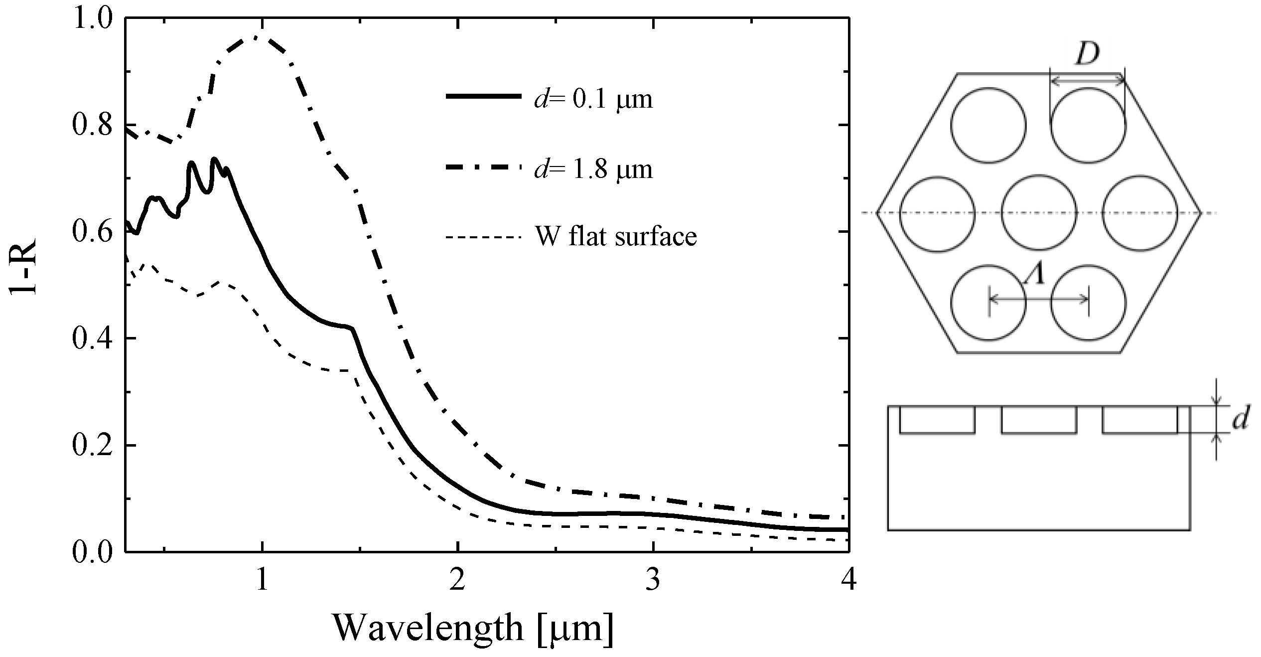
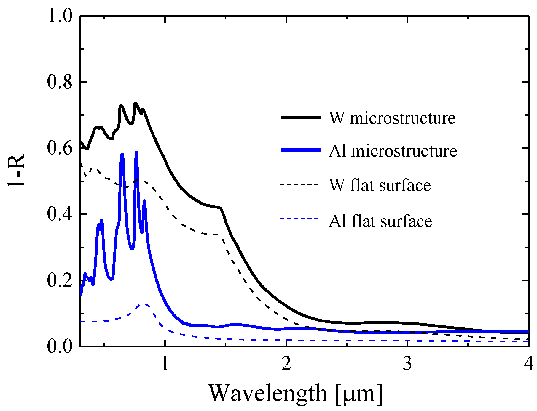
Optical simulations were conducted for honeycomb array cylindrical microcavities to determine their potential as solar-selective absorbers. The rigorous coupled-wave analysis (RCWA) method was applied to simulate their absorbance spectra [20]. In all the simulations in this research, optical constants at room temperature were applied. The simulated absorbance spectra varying with the cylindrical microcavity depth are shown in Figure 1 and the simulated model is shown in the insert. For the deep microcavity model, numerous peaks related to the confinement effect in a cylindrical microcavity possess a high and broad absorbance peak. In contrast, the shallow microcavity model also reveals an absorbance enhancement, but the intensity of the absorbance peak is much smaller than that of the deep microcavity model. Ghebrebrhan et al. reported that it is essential to make a Q-matching condition, where the losses of radiation through the top, and absorption on the side walls and bottom, are equal in a microcavity, for high-intensity absorbance peaks. This condition usually obtained by the deep microcavity [21]. Sai et al. also indicated from numerical simulation results that the microcavity effect cannot be seen in a shallow microcavity but is strongly observed in a deep microcavity [22]. Figure 2 shows the contribution of the substrate optical property to the absorption property. Large differences in absorbance intensities in the short wavelength range can be recognized in W and Al microstructures, even though they possess the same geometries. It is explained that confinement effect in shallow microcavity is weak. Therefore, the contribution from the substrate property is largely appears in the shallow microcavity.

Figure 1.
Simulated absorbance spectra of shallow (d = 0.1 μm) and deep (d = 1.8 μm) cylindrical microcavity. Pitch Λ and diameter D of the microcavities are fixed at 0.8 and 0.6 μm, respectively.

Figure 2.
Simulated absorbance spectra of shallow cylindrical microcavity with Λ = 0.8 μm, D = 0.6 μm, and d = 0.1 μm fabricated on W or Al substrate (Solid lines). Absorbance spectra with flat surface on each material is also shown (dashed lines).
2.2. Fabrication of Honeycomb Array Shallow Cylindrical Microcavity
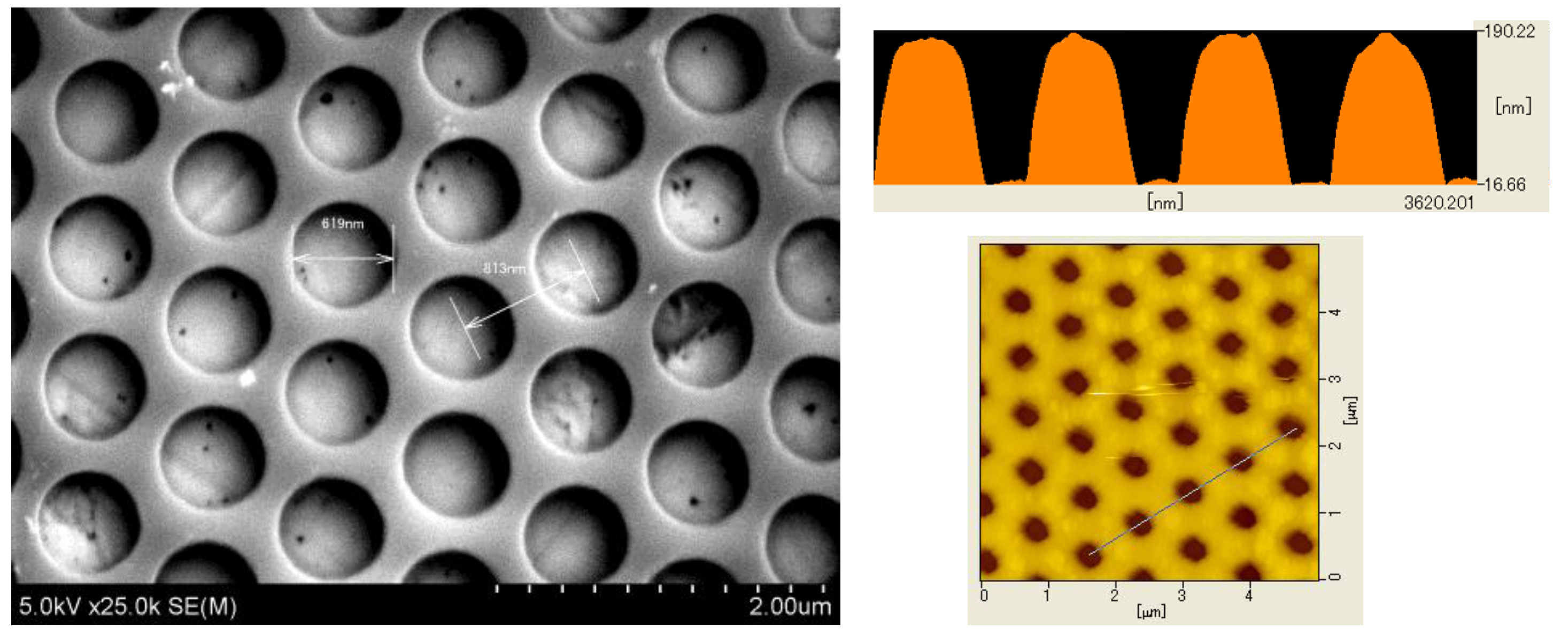
Honeycomb array cylindrical microcavities were fabricated on a polycrystalline tungsten (W) substrate (99.95%; The Nilaco Co., Tokyo, Japan). Interference lithography techniques were applied to transfer the periodic pattern into a resist mask. Due to the low-cost nature of this technique from not utilizing an expensive exposure machine, it is potentially suited for large-area fabrication [23,24,25]. Honeycomb-arrayed periodic patterns were fabricated on the resist mask by three-beam interference lithography using Mach-Zehnder type optics [26]. The conditions of the interference lithograph were used as stated in the previous report [27]. After the lithography process, the resist pattern was transferred onto the W substrate by conducting a dry etching process with fast ion beam (FAB) etching. This etching was performed with sulfur hexafluoride (SF6) gas under an applied voltage of 3.0 kV for ion acceleration. After the dry etching process, the remaining resists were rinsed in acetone. The fabricated microstructures were observed for their surface geometry by scanning electron microscope (SEM) and contact-mode atomic force microscope (AFM; SPI-4000, Seiko Instruments Inc., Tokyo, Japan) as shown in Figure 3. The diameter of a cylindrical microcavity and period length measured from the SEM image were 0.62 and 0.81 μm, respectively. Depth of the microcavity as measured by AFM was 0.17 μm. The absorbance spectrum of the sample was calculated from the measured reflectance spectrum using a spectrometer in the wavelength range from 0.3 to 1.75 μm (Lambda 900, PerkinElmer Japan, Tokyo, Japan) and FT-IR (Spectrum GX, PerkinElmer Japan, Tokyo, Japan) from 1.75 to 10 μm. In both measurements, integrating spheres are applied. The inside of the integrating spheres are coated with high-reflectivity materials, which enable us to correct reflected light in all direction. Therefore, hemispherical reflectance can be measured with this method. The measured result is shown in Figure 4 and compares the simulated results with a different depth. Both the measured absorbance spectrum and the simulated result for the 0.1 μm depth model are similar, although the actual depth was measured as 0.17 μm. This may be caused by the difference of the microcavity shape between the experiment and the simulation. To evaluate the performance of these materials as solar selective absorbers, a figure of merit was calculated from the following formulae and reference [28] was applied:

Figure 3.
A SEM image of fabricated cylindrical microcavity (Left) and surface profile measured by contact-mode AFM (Right).
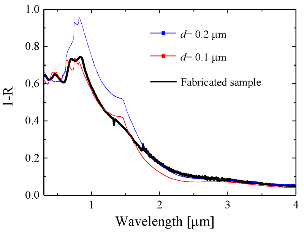
Figure 4.
Measured spectra obtained by reflectance measurement at room temperature are shown by the black solid line. Simulated absorbance spectra with different depth of the microcavity are shown by the red line (d = 0.1 μm), and the blue line (d = 0.2 μm). Pitch Λ and diameter D of the microcavities are fixed at 0.8 and 0.6 μm, respectively, in the simulation.
In this formula, C shows the solar concentration ratio, ibb shows spectral emissive power of a blackbody, and isol shows spectral solar energy of AM1.5. Integrating intervals were taken at a sufficient range, which were from 0.3 to 4 μm and 0.3 to 10 μm for αsol and εht, respectively. Solar absorbance αsol and hemispherical total emittance εht(T) are defined by Equations (2) and (3), respectively:
In these formulae, α(λ) and ε(λ) show spectral absorbance and spectral emittance of a solar-selective absorber. By Kirchhoff’s Law, α(λ) can be regarded as ε(λ).
The figure of merits η is only 0.56 with a condition under solar concentration ratio C = 100 at 700 °C due to a low solar absorbance αsol of 0.59, even though it shows low hemispherical total emittance εht of 0.07. To attain high η, a high αsol with a low εht is required. To obtain high αsol, it is essential to broaden the high absorbance range and increase absorbance intensity within the solar spectrum range.
3. Honeycomb Array Cylindrical Microcavity with Multilayer Coating
3.1. Numerical Simulation
To increase αsol, we considered fabricating a metal-dielectric multi-layer on shallow microcavity structures. It is reported that the multi-layer consisting of a nano-metal thin film sandwiched between transparent dielectric layers shows high spectrally-selective absorption properties [29]. In this simulation, the multi-layer consists of Pt thin film and Al2O3 layers. In the experiment, multi-layers were fabricated by an ALD method. Pt and Al2O3 were selected as composition materials of because the fabrication techniques of these materials regarding the ALD process have been well researched and already established [30,31,32,33].
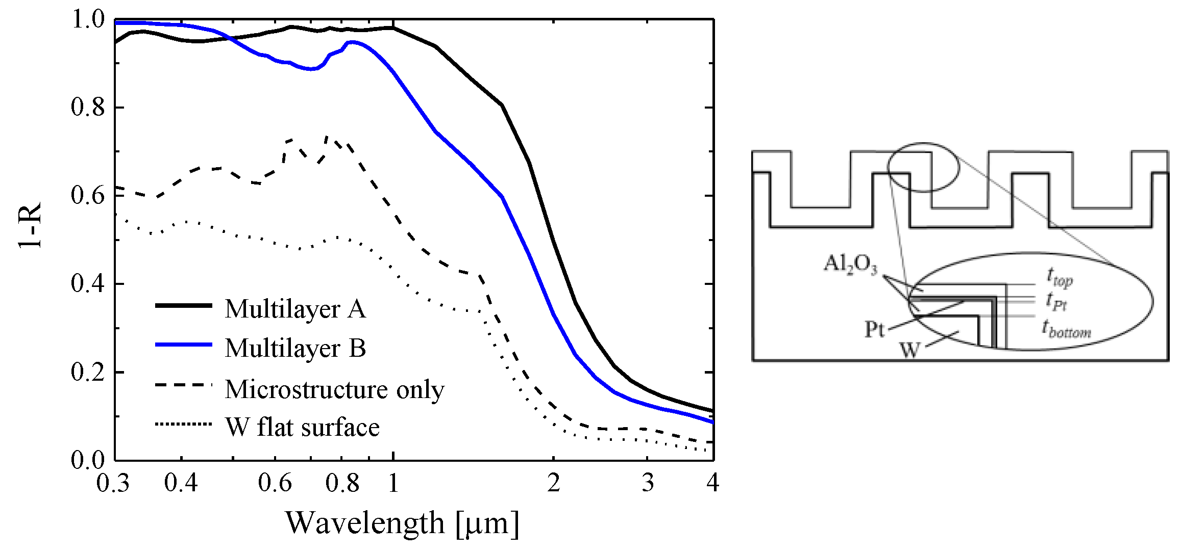
Substrate properties play a very important role in shallow microstructures, compared to the confined effect of radiation in the microcavity as indicated above. Therefore, we thought that high spectrally-selective absorption properties would be obtained, even with shallow microcavities, by controlling the substrate property with multi-layers. Two results of the simulation with two different absorbers, which possess the same microstructure but different multilayers are shown in Figure 5: (A) ttop/tPt/tbottom = 55/4/50 nm and (B) ttop/tPt/tbottom = 30/4/40 nm. Each layer thickness in multilayer (A) was optimized to get the highest η at 700 °C under C = 100. By the contrast, multilayer (B) is just for comparison to show the contribution of multilayer property. Absorbance is drastically increased in the short wavelength range compared to that of microstructures without a multi-layer coating. Due to interference in the multi-layer, a difference in dielectric layer thickness corresponds to an absorbance spectrum shape in the short wavelength range and a cut-off position as shown in Figure 5. However, absorbance enhancement at approximately the 1 μm range cannot be explained because, in this range, only small absorbance enhancements have been shown. One of the causes would be an increase of optical length inside a microcavity. In this simulation, depth of microcavity is set to be 0.1 μm and the total thickness of the multi-layer is roughly 0.1 μm, in the case of multilayer (A). This translate into a micro-hole occupied with mostly Al2O3 of which the refractive index is 1.7 in this wavelength range. An increase of the refractive index causes a shift of the absorbance peak corresponding to the confined effect in a microcavity. Therefore, this peak shift would also contribute to an increase in absorbance near 1 μm.
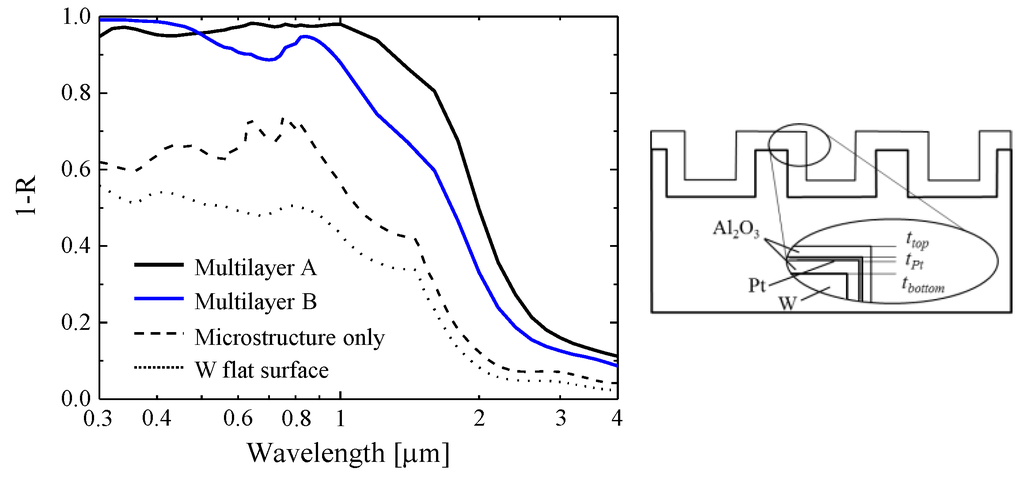
Figure 5.
Simulated absorbance spectra of cylindrical microcavity with multilayer coating. A schematic illustration of the model is shown in the inset. Black solid line shows the microstructure with multilayer (A) in which each thickness is ttop/tPt/tbottom = 55/4/50 nm. The blue solid line shows the microstructure with multilayer (B) in which each thickness is ttop/tPt/tbottom = 30/4/40 nm. The dashed line shows the W cylindrical microcavity with Λ = 0.8 μm, D= 0.6 μm, and d = 0.1 μm. The dotted line shows the W intrinsic property at flat surface.
3.2. Fabrication of Honeycomb Array Cylindrical Microcavity with Multilayer Coating
The multi-layer was fabricated with ALD process. In this process, trimethylaluminum ((CH3)3Al) and trimethyl(methylcyclopentadienyl)-platinum (MeCpPtMe3), were used as precursors for Al2O3 and Pt, respectively. During the process, the sample stage was heated to 200 °C for Al2O3 and 280 °C for Pt fabrication. The deposition rate of Al2O3 and Pt were 15.6 and 5 nm, each with 100 cycles, respectively. Sufficient bulb open time was defined by estimating enough of the amount of molecules which cover the substrate surface. Then, the multi-layer was deposited onto the W with honeycomb array cylindrical cavities, which is shown in Section 2. A planar view of the material taken by SEM, along with a surface profile with AFM are demonstrated in Figure 6. The coating process with the multi-layer enlarged the side-wall width but decreased the diameter of a cylindrical cavity, compared to Figure 3, while the depth of a cylindrical cavity still shows 170 nm, which is the same as the non-coated sample. This highlights the idea that utilizing ALD allows for a conformal multi-layer that can be fabricated onto microstructures.
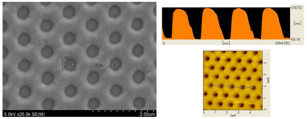
Figure 6.
A SEM image of fabricated cylindrical microcavity coated with the multilayer (Left) and surface profile measured by contact-mode AFM (Right).
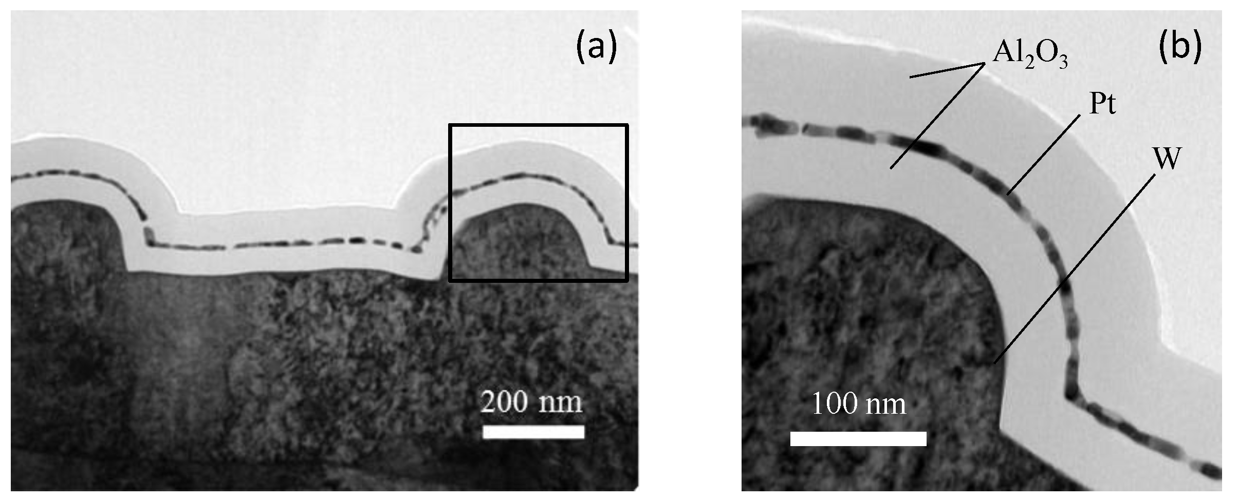
To clearly see a configuration of the multi-layer on microstructures, a transmission electron microscope (TEM) was used to observe the cross-sectional view of the film. Figure 7a shows a cylindrical cavity, where the side walls are not vertical to the bottom and the corners at the top walls are relatively rounded. This morphology would likely affect the degradation of the confinement effect within the cavity. Therefore, it shows an almost similar absorbance spectrum compared to the simulated spectrum where the cavity depth is equal to 100 nm, even though the actual cavity depth is 170 nm.

Figure 7.
(a) Cross-sectional view of the fabricated cylindrical microcavity coated with the multilayer taken by TEM. (b) The high-magnification of the marked part in (a).
For the multi-layer, highly uniform coatings can be realized on the microstructures. Each layer completely follows the curve on the microstructures. Therefore, each layer thickness is the same in all locations as we expected. However, it can be seen in Figure 7b that, for the thin Pt film, a continuous deposition is not present. The Pt layer should occur as island growth, as described by the Volmer-Weber growth mode [34] on amorphous Al2O3 layer. The 4 nm Pt film was a non-uniform film with a thickness that was double than the expected thickness. Although Pt thin film is not fabricated continuously, the measured absorbance spectrum shows high-consistency as shown in Figure 8. It is likely that this non-uniform film plays the role of a continuous thin film in terms of optical characteristics.
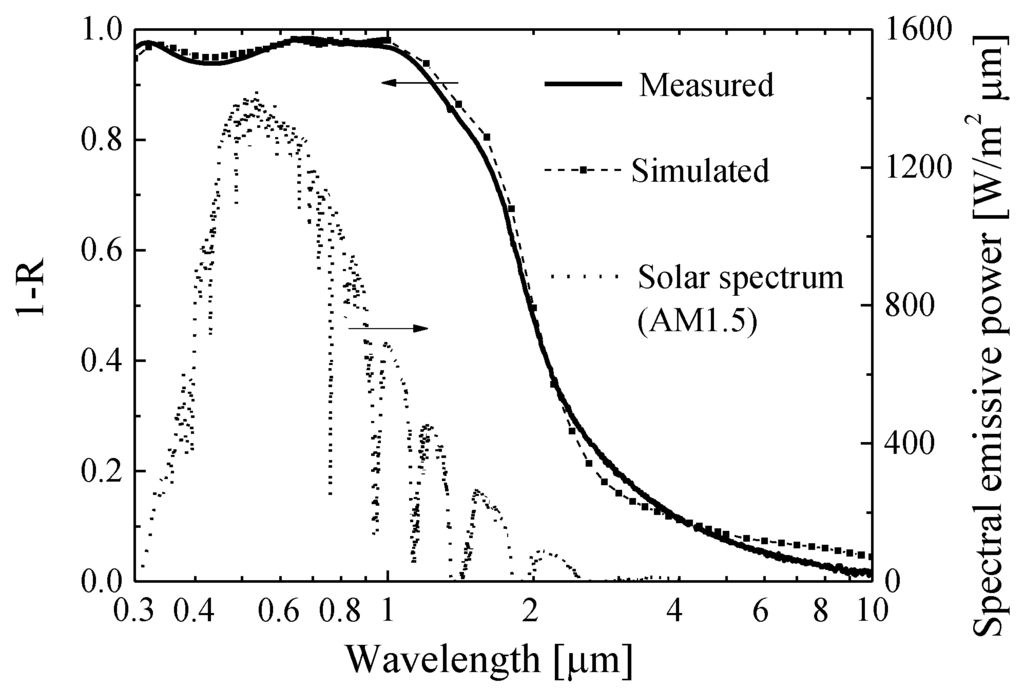
Figure 8.
Measured absorbance of cylindrical microcavity coated with multilayer at room temperature. Simulated results are shown by dashed line with square dots. In the simulation size of microcavity is Λ = 0.8 μm, D = 0.6 μm and d = 0.1 μm, and each thickness of the multilayer is ttop/tPt/tbottom = 55/4/50 nm. A dotted line shows the solar spectrum of AM1.5.
3.3. Evaluation of the Performance
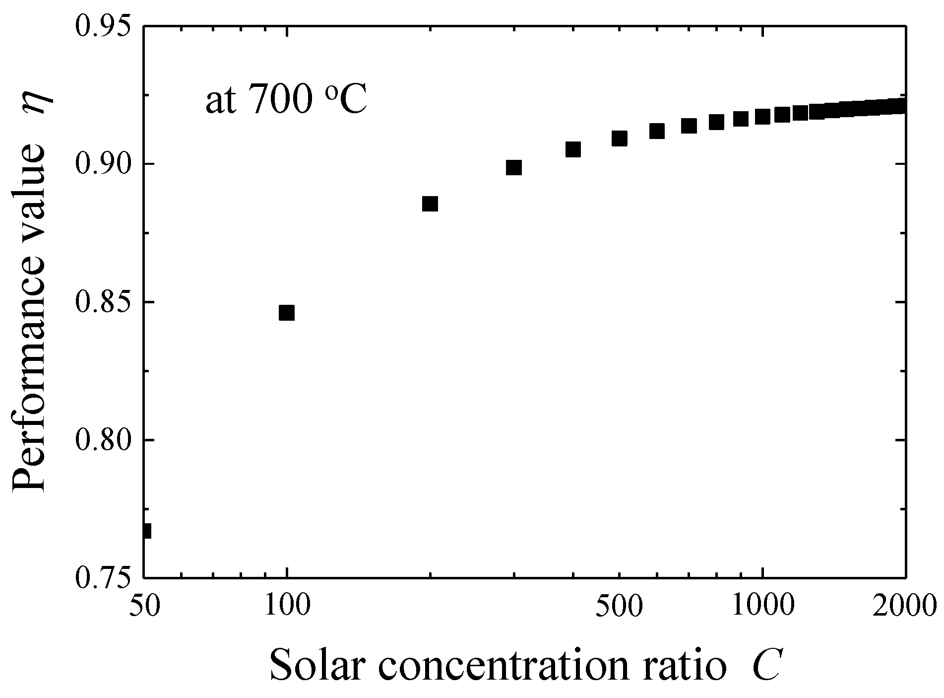
The performance of the fabricated absorber with multi-layer coated microstructures was evaluated as a function of the solar concentration ratio C, which is plotted in Figure 9. With contributions of both broad and high-absorbance in the short wavelength range, a much higher solar absorbance αsol of 0.92 can be obtained. Whereas hemispherical emittance εht at 700 °C still maintains a low value of 0.18 due to a steep optical cutoff property. Finally, the performance value η under C = 100 becomes 0.84. Generally at a high-temperature range of more than 700 °C, it is difficult to obtain a high-performance value (>0.80) due to difficulty in realizing high-absorbance and low-emittance simultaneously, separated by a proper cut-off position. However, this absorber can reach the performance as high as that of the previously-reported absorbers. As shown in Figure 9, due to its high solar absorbance αsol, this absorber shows higher η at a high solar concentration condition, such as using large aperture trough mirrors.
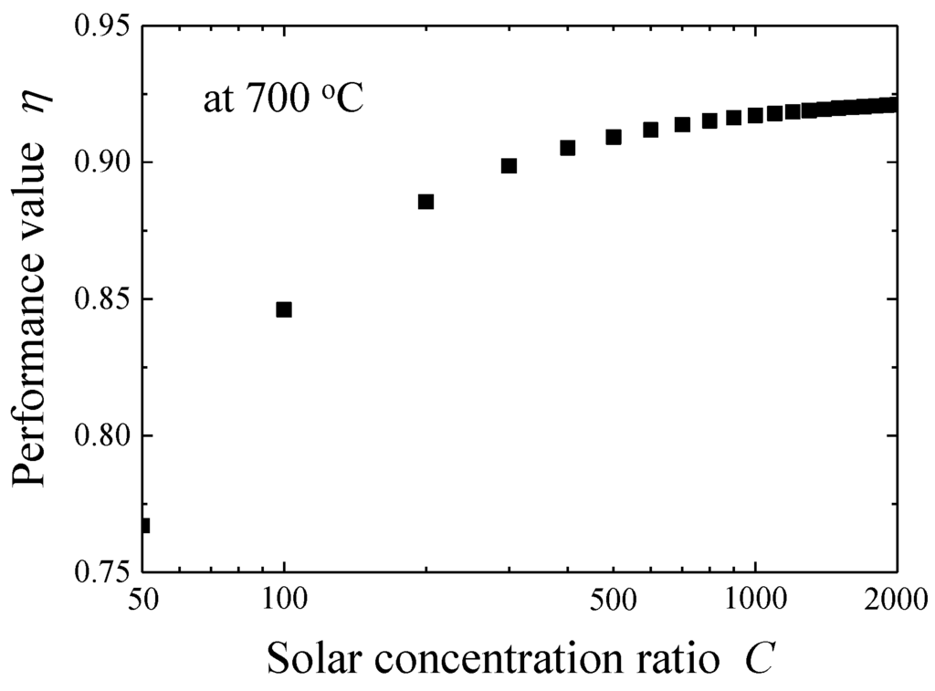
Figure 9.
Calculated performance value η of a fabricated sample as a function of solar concentration ratio C at 700 °C.
3.4. Thermal Stability Test
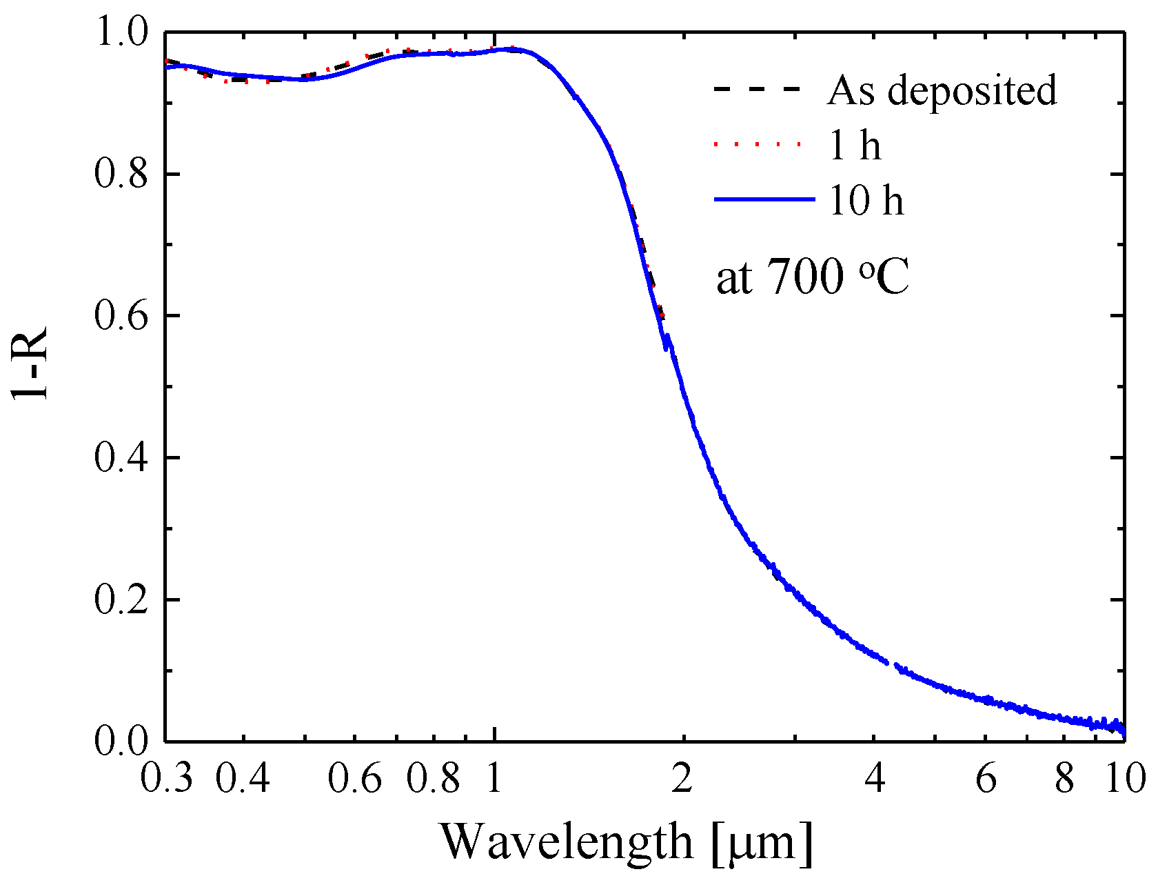
Thermal stability was verified with an infrared lamp furnace under vacuum. Vacuum levels were kept at approximately 1 Pa; i.e., oxygen partial pressure is approximately 0.2 Pa, during the entire test. Usually, glass absorber tubes used for trough systems keep pressure as low as 0.1 Pa. Therefore, it can be said that the test was performed in more severe conditions. The fabricated absorber sample was heated up to 700 °C with a heating slope of 28 °C/min. After the sample was kept at 700 °C for several hours, it was cooled down with the same temperature slope. The absorbance spectra measured after heating for 1 and 10 h are shown in Figure 10. Even after heating for 10 h, no change was observed regarding the absorbance property. Therefore, it can be concluded that the material is stable at temperatures of 700 °C. A longer test length would confirm further durability.

Figure 10.
Measured absorbance spectra of the samples at room temperature as deposited, after 1 h heating, and 10 h heating at 700 °C under vacuum.
4. Conclusions
Surface microstructures fabricated on refractory metals are a promising technology to control thermal radiation at high temperatures. However, this technique is typically not well-suited because deep microstructures should be required to attain high spectrally-selective absorption properties. In this study, we have investigated high spectrally-selective absorption properties; i.e., broad and high-absorbance in a short wavelength range and low emittance in a long wavelength range, with shallow honeycomb array cylindrical microcavities coated by metal-dielectric multi-layers.
A honeycomb array cylindrical microcavity was fabricated based on interference lithography and normal dry etching processes. The multilayer consist of 4 nm Pt thin film sandwiched with Al2O3 layers were fabricated with the atomic layer deposition (ALD) method. Due to a high conformal multilayer on the cylindrical microcavity, thanks to characteristics of the ALD method, the absorbance spectrum is consistent with the simulated result.
Our material revealed a high performance value η = 0.84 at the condition of 700 °C under a solar concentration ratio C = 100 due to high solar absorbance αsol = 0.92 and low hemispherical total emittance εht = 0.18. Finally, thermal stability was confirmed at 700 °C under vacuum within a pressure range of 1 Pa.
The periodic shallow microstructures coated by multi-layers shows high spectral selectivity and high thermal stability. The technique used for fabrication has possibilities for large-area fabrication. Therefore, this technology may impact system efficiency improvement for solar thermal energy utilization systems such as CSP, solar thermochemical conversion systems, solar-thermophotovoltaic systems, etc.
Acknowledgments
This study was supported by JST-ALCA and JSPS KAKENHI Grant Numbers 15K13395, 26820055. I also would like to appreciate. Kumano and Hikichi for contribution of ALD fabrication.
Author Contributions
Makoto Shimizu, Fumitada Iguchi and Hiroo Yugami conceived and designed the experiments; Makoto Shimizu and Hiroki Akutsu performed the numerical simulations; Hiroki Akutsu performed most part of the fabrication; Shinichiro Tsuda operated the ALD processes; Makoto Shimizu and Hiroki Akutsu analyzed the data; M. Shimizu wrote the paper.
Conflicts of Interest
The authors declare no conflict of interest.
References
- Giostri, A.; Binotti, M.; Astolfi, M.; Silva, P.; Macchi, E.; Manzolini, G. Comparison of different solar plants based on parabolic trough technology. Sol. Energy 2012, 86, 1208–1221. [Google Scholar] [CrossRef]
- Pavlović, T.M.; Radonjić, I.S.; Milosavljević, D.D.; Pantić, L.S. A review of concentrating solar power plants in the world and their potential use in Serbia. Renew. Sustain. Energy Rev. 2012, 16, 3891–3902. [Google Scholar] [CrossRef]
- Tian, Y.; Zhao, C.Y. A review of solar collectors and thermal energy storage in solar thermal applications. Appl. Energy 2013, 104, 538–553. [Google Scholar] [CrossRef]
- Maccari, A.; Bissi, D.; Casubolo, G.; Guerrini, F.; Lucatello, L.; Luna, G.; Zuanella, M. Archimede Solar Energy Molten Salt Parabolic Trough Demo Plant: A Step Ahead towards the New Frontiers of CSP. Energy Procedia 2015, 69, 1643–1651. [Google Scholar] [CrossRef]
- Tanaka, Y.; Tarutani, Y.; Magoshi, R.; Nakano, T. Feature and Operating Experience of 1000 MW Class Steam Turbine with Highest Efficiency in the World. Mitsubishi Juko Giho 2002, 39, 132–135. [Google Scholar]
- Agüero, A.; Muelas, R.; Pastor, A.; Osgerby, S. Long exposure steam oxidation testing and mechanical properties of slurry aluminide coatings for steam turbine components. Surf. Coat. Technol. 2005, 200, 1219–1224. [Google Scholar] [CrossRef]
- Gubbels, G.H.M.; Wolff, L.R.; Metselaar, R. A thermionic energy converter with a molybdenum-alumina cermet emitter. J. Appl. Phys. 1990, 68, 5856–5865. [Google Scholar] [CrossRef]
- Zhang, Q.C.; Yin, Y.B.; Mills, D.R. High efficiency Mo-Al2O3 cermet selective surfaces for high-temperature application. Sol. Energy Mater. Sol. Cells 1996, 40, 43–53. [Google Scholar] [CrossRef]
- Zhang, Q.C. Stainless-steel-AlN cermet selective surfaces deposited by direct current magnetron sputtering technology. Sol. Energy Mater. Sol. Cells 1998, 52, 95–106. [Google Scholar] [CrossRef]
- Barshilia, H.C.; Selvakumar, N.; Vignesh, G.; Rajam, K.S.; Biswas, A. Optical properties and thermal stability of pulsed-sputter-deposited AlxOy/Al/AlxOy multilayer absorber coatings. Sol. Energy Mater. Sol. Cells 2009, 93, 315–323. [Google Scholar] [CrossRef]
- Selvakumar, N.; Barshilia, H.C.; Rajam, K.S.; Biswas, A. Structure, optical properties and thermal stability of pulsed sputter deposited high temperature HfOx/Mo/HfO2 solar selective absorbers. Sol. Energy Mater. Sol. Cells 2010, 94, 1412–1420. [Google Scholar] [CrossRef]
- Chester, D.; Bermel, P.; Joannopoulos, J.D.; Soljacic, M.; Celanovic, I. Design and global optimization of high-efficiency solar thermal systems with tungsten cermets. Opt. Express 2011, 19, A245–A257. [Google Scholar] [CrossRef] [PubMed]
- Selvakumar, N.; Manikandanath, N.T.; Biswas, A.; Barshilia, H.C. Design and fabrication of highly thermally stable HfMoN/HfON/Al2O3 tandem absorber for solar thermal power generation applications. Sol. Energy Mater. Sol. Cells 2012, 102, 86–92. [Google Scholar] [CrossRef]
- Maruyama, S.; Kashiwa, T.; Yugami, H.; Esashi, M. Thermal radiation from two-dimensionally confined modes in microcavities. Appl. Phys. Lett. 2001, 79, 1393–1395. [Google Scholar] [CrossRef]
- Sai, H.; Kanamori, Y.; Yugami, H. High-temperature resistive surface grating for spectral control of thermal radiation. Appl. Phys. Lett. 2003, 82, 1685–1687. [Google Scholar] [CrossRef]
- Sai, H.; Yugami, H.; Kanamori, Y.; Hane, K. Solar selective absorbers based on two-dimensional W surface gratings with submicron periods for high-temperature photothermal conversion. Sol. Energy Mater. Sol. Cells 2003, 79, 35–49. [Google Scholar] [CrossRef]
- Rinnerbauer, V.; Yeng, Y.X.; Chan, W.R.; Senkevich, J.J.; Joannopoulos, J.D.; Soljačić, M.; Celanovic, I. High-temperature stability and selective thermal emission of polycrystalline tantalum photonic crystals. Opt. Express 2013, 21, 11482–11491. [Google Scholar] [CrossRef] [PubMed]
- Wang, H.; Wang, L. Perfect selective metamaterial solar absorbers. Opt. Express 2013, 21, A1078–A1093. [Google Scholar] [CrossRef] [PubMed]
- Shemelya, C.; DeMeo, D.; Latham, N.P.; Wu, X.; Bingham, C.; Padilla, W.; Vandervelde, T.E. Stable high temperature metamaterial emitters for thermophotovoltaic applications. Appl. Phys. Lett. 2014, 104, 201113. [Google Scholar] [CrossRef]
- Moharam, M.G.; Gaylord, T.K. Rigorous coupled-wave analysis of planar-grating diffraction. J. Opt. Soc. Am. B Opt. Phys. 1981, 71, 811–818. [Google Scholar] [CrossRef]
- Ghebrebrhan, M.; Bermel, P.; Yeng, Y.X.; Celanovic, I.; Soljačić, M.; Joannopoulos, J.D. Tailoring thermal emission viaQmatching of photonic crystal resonances. Phys. Rev. B Condens. Matter. 2011, 83, 033810. [Google Scholar] [CrossRef]
- Sai, H.; Kanamori, Y.; Yugami, H. Tuning of the thermal radiation spectrum in the near-infrared region by metallic surface microstructures. J. Micromech. Microeng. 2005, 15, S243–S249. [Google Scholar] [CrossRef]
- Savas, T.A.; Schattenburg, M.L.; Carter, J.M.; Smith, H.I. Large-area achromatic interferometric lithography for 100 nm period gratings and grids. J. Vac. Sci. Technol. B 1996, 14, 4167–4170. [Google Scholar] [CrossRef]
- Chen, C.G.; Konkola, P.T.; Heilmann, R.K.; Joo, C.; Schattenburg, M.L. Nanometer-accurate grating fabrication with scanning beam interference lithography. In Proceedings of the SPIE’s International Symposium on Smart Materials, Nano-, and Micro-Smart Systems, Melbourne, Australia, 16 December 2002; Volume 4936, pp. 126–134.
- Si, G.; Wang, Q.; Lv, J.; Miao, L.; Wang, F.; Peng, S. Interference lithography patterned large area plasmonic nanodisks for infrared detection. Mater. Lett. 2014, 128, 373–375. [Google Scholar] [CrossRef]
- De Boor, J.; Geyer, N.; Gösele, U.; Schmidt, V. Three-beam interference lithography: Upgrading a Lloyd’s interferometer for single-exposure hexagonal patterning. Opt. Lett. 2009, 34, 1783–1785. [Google Scholar] [CrossRef] [PubMed]
- Shimizu, M.; Yamada, T.; Sasaki, K.; Takada, A.; Nomura, H.; Iguchi, F.; Yugami, H. Anisotropic multi-step etching for large-area fabrication of surface microstructures on stainless steel to control thermal radiation. Sci. Technol. Adv. Mater. 2016, 16, 025001. [Google Scholar] [CrossRef]
- Hall, A.C.; Ambrosini, A.; Ho, C.K.; McCloskey, J.F.; van Every, K.; McCloskey, J.F.; Urrea, D.A.; Lambert, T.N.; Bencomo, M.; Mahoney, A.R.; et al. Solar Selective Coatings for Concentrating Solar Power Central Receivers. Adv. Mater. Process. 2012, 170, 28–32. [Google Scholar]
- Shimizu, M.; Kohiyama, A.; Yugami, H. High-efficiency solar-thermophotovoltaic system equipped with a monolithic planar selective absorber/emitter. J. Photonics Energy 2015, 5, 053099. [Google Scholar] [CrossRef]
- Aaltonen, T.; Ritala, M.; Sajavaara, T.; Keinonen, J.; Leskelä, M. Atomic layer deposition of platinum thin films. Chem. Mater. 2003, 15, 1924–1928. [Google Scholar] [CrossRef]
- Aaltonen, T.; Ritala, M.; Tung, Y.L.; Chi, Y.; Arstila, K.; Meinander, K.; Leskelä, M. Atomic layer deposition of noble metals: Exploration of the low limit of the deposition temperature. J. Mater. Res. 2004, 19, 3353–3358. [Google Scholar] [CrossRef]
- Juppo, M.; Rahtu, A.; Ritala, M.; Leskelä, M. In situ mass spectrometry study on surface reactions in atomic layer deposition of Al2O3 thin films from trimethylaluminum and water. Langmuir 2000, 16, 4034–4039. [Google Scholar] [CrossRef]
- Elam, J.W.; Routkevitch, D.; Mardilovich, P.P.; George, S.M. Conformal coating on ultrahigh-aspect-ratio nanopores of anodic alumina by atomic layer deposition. Chem. Mater. 2003, 15, 3507–3517. [Google Scholar] [CrossRef]
- Shrestha, P.; Gu, D.; Tran, N.; Tapily, K.; Baumgart, H.; Namkoong, G. Investigation of Volmer-Weber Growth during the Nucleation Phase of ALD Platinum Thin Films and Template Based Platinum Nanotubes. ECS Trans. 2010, 33, 127–134. [Google Scholar]
© 2016 by the authors; licensee MDPI, Basel, Switzerland. This article is an open access article distributed under the terms and conditions of the Creative Commons by Attribution (CC-BY) license (http://creativecommons.org/licenses/by/4.0/).

