Increasing Surface Plasmons Propagation via Photonic Nanojets with Periodically Spaced 3D Dielectric Cuboids


Abstract
:
1. Introduction
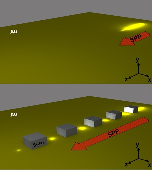
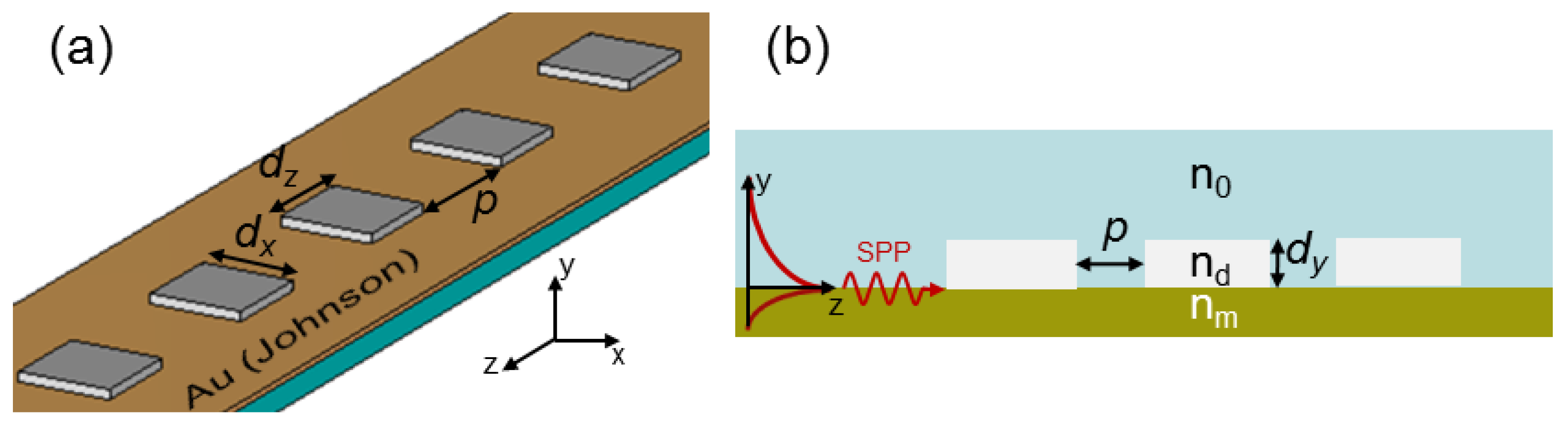
2. Design
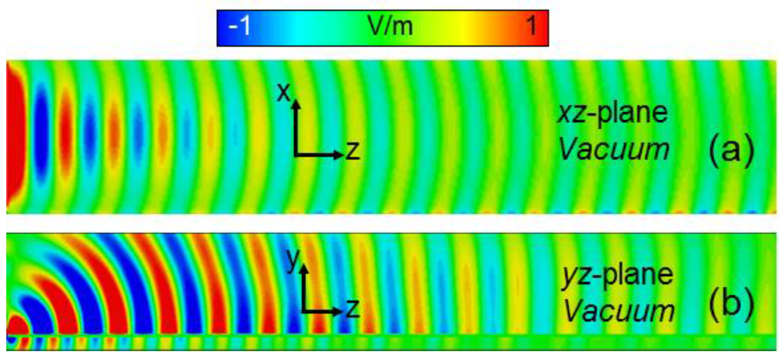
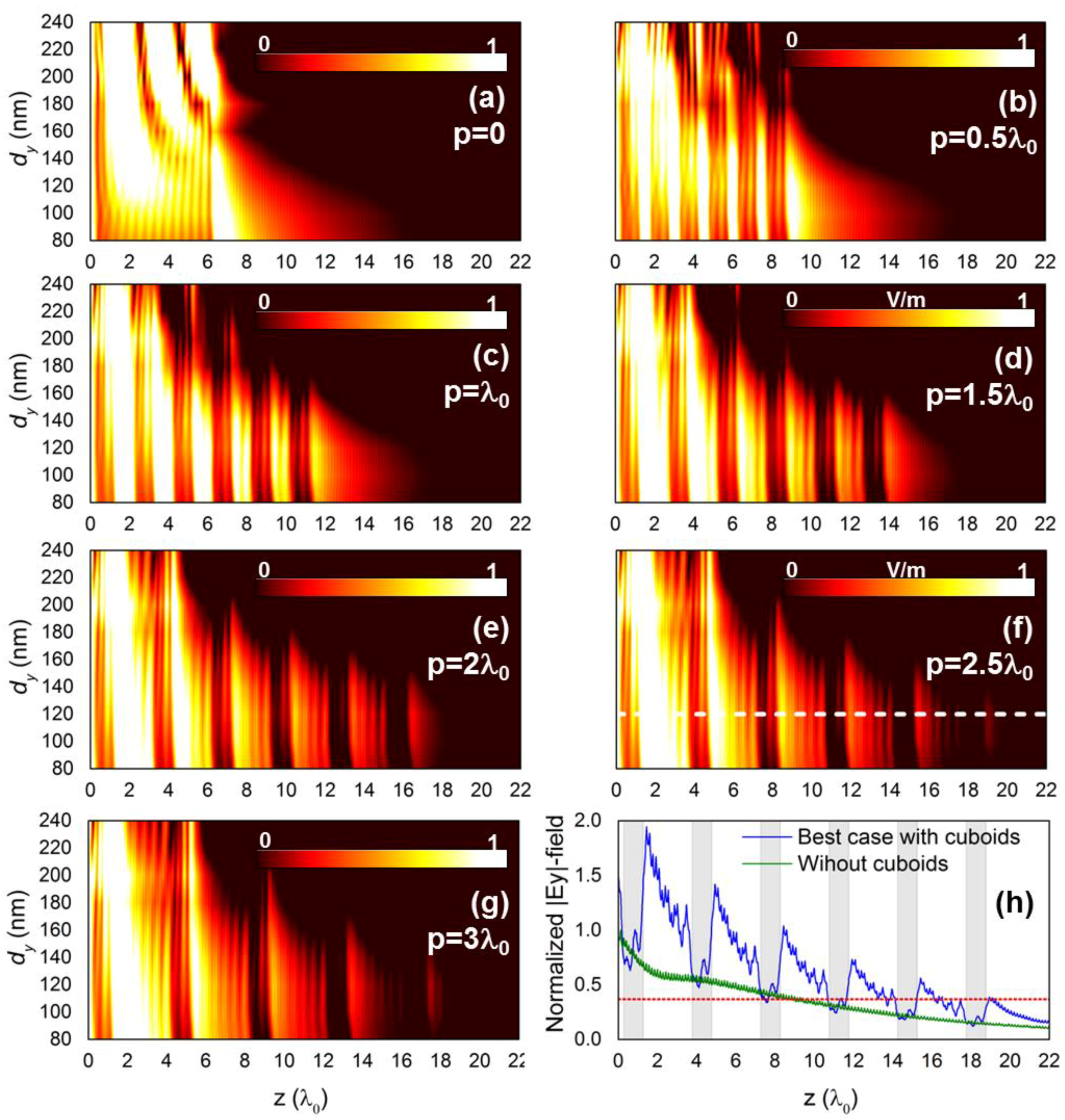
3. Results and Discussion
4. Conclusions
Acknowledgments
Author Contributions
Conflicts of Interest
Abbreviations
| PNJ | Photonic Nanojet |
| SPP | Surface Plasmon |
| FWHMx | Full-width at half-maximum along the transversal x-axis |
References
- Born, M.; Wolf, E. Principles of Optics, 7th ed.; Cambridge University Press: New York, NY, USA, 1999. [Google Scholar]
- Pendry, J.B. Negative refraction makes a perfect lens. Phys. Rev. Lett. 2000, 85, 3966–3969. [Google Scholar] [CrossRef] [PubMed]
- Grbic, A.; Eleftheriades, G.V. Overcoming the Diffraction Limit with a Planar Left-Handed Transmission-Line Lens. Phys. Rev. Lett. 2004, 92, 117401–117403. [Google Scholar] [CrossRef] [PubMed]
- Jacob, Z.; Alekseyev, L.V.; Narimanov, E. Optical Hyperlens: Far-field imaging beyond the diffraction limit. Opt. Express 2006, 14, 8247–8256. [Google Scholar] [CrossRef] [PubMed]
- Liu, Z.; Lee, H.; Xiong, Y.; Sun, C.; Zhang, X. Far-field optical hyperlens magnifying sub-diffraction-limited objects. Science 2007, 315, 1686. [Google Scholar] [CrossRef] [PubMed]
- Huang, F.M.; Zheludev, N.I. Super-resolution without evanescent waves. Nano Lett. 2009, 9, 1249–1254. [Google Scholar] [CrossRef] [PubMed]
- Rogers, E.T.F.; Lindberg, J.; Roy, T.; Savo, S.; Chad, J.E.; Dennis, M.R.; Zheludev, N.I. A super-oscillatory lens optical microscope for subwavelength imaging. Nat. Mater. 2012, 11, 432–435. [Google Scholar] [CrossRef] [PubMed]
- Wang, Z.; Guo, W.; Li, L.; Luk’yanchuk, B.; Khan, A.; Liu, Z.; Chen, Z.; Hong, M. Optical virtual imaging at 50 nm lateral resolution with a white-light nanoscope. Nat. Commun. 2011, 2, 218. [Google Scholar] [CrossRef] [PubMed]
- Hao, X.; Kuang, C.; Liu, X.; Zhang, H.; Li, Y. Microsphere based microscope with optical super-resolution capability. Appl. Phys. Lett. 2011, 99, 203102. [Google Scholar] [CrossRef]
- Li, X.; Chen, Z.; Taflove, A.; Backman, V. Optical analysis of nanoparticles via enhanced backscattering facilitated by 3-D photonic nanojets. Opt. Express 2005, 13, 526–533. [Google Scholar] [CrossRef] [PubMed]
- Heifetz, A.; Huang, K.; Sahakian, A.V.; Li, X.; Taflove, A.; Backman, V. Experimental confirmation of backscattering enhancement induced by a photonic jet. Appl. Phys. Lett. 2006, 89, 221118. [Google Scholar] [CrossRef]
- Heifetz, A.; Kong, S.-C.; Sahakian, A.V.; Taflove, A.; Backman, V. Photonic Nanojets. J. Comput. Theor. Nanosci. 2009, 6, 1979–1992. [Google Scholar] [CrossRef] [PubMed]
- Liu, C.; Chang, L.; Yang, L. Photonic Nanojet in Non-spherical Micro-particles. In Proceedings of the 9th IEEE International Conference on Nano/Micro Engineered and Molecular Systems (NEMS), Waikiki Beach, HI, USA, 13–16 April 2014; pp. 536–539.
- Mao, X.; Yang, Y.; Dai, H.; Luo, D.; Yao, B.; Yan, S. Tunable photonic nanojet formed by generalized Luneburg lens. Opt. Express 2015, 23, 26426. [Google Scholar] [CrossRef] [PubMed]
- Smolyaninova, V.; Lahneman, D.; Adams, T.; Gresock, T.; Zander, K.; Jensen, C.; Smolyaninov, I. Experimental Demonstration of Luneburg Waveguides. Photonics 2015, 2, 440–448. [Google Scholar] [CrossRef]
- Liu, C. Ultra-elongayed photonic nanojets generated by a graded-index microellipsoid. Prog. Electromagn. Res. Lett. 2013, 37, 153–165. [Google Scholar] [CrossRef]
- Born, B.; Krupa, J.D.; Geoffroy-Gagnon, S.; Holzman, J.F. Integration of photonic nanojets and semiconductor nanoparticles for enhanced all-optical switching. Nat. Commun. 2015, 6, 8097. [Google Scholar] [CrossRef] [PubMed]
- Pacheco-Peña, V.; Beruete, M.; Minin, I.V.; Minin, O.V. Terajets produced by dielectric cuboids. Appl. Phys. Lett. 2014, 105, 084102. [Google Scholar] [CrossRef]
- Pacheco-Peña, V.; Beruete, M.; Minin, I.V.; Minin, O.V. Multifrequency focusing and wide angular scanning of terajets. Opt. Lett. 2015, 40, 245–248. [Google Scholar] [CrossRef] [PubMed]
- Minin, I.V.; Minin, O.V.; Pacheco-Peña, V.; Beruete, M. Localized photonic jets from flat, three-dimensional dielectric cuboids in the reflection mode. Opt. Lett. 2015, 40, 2329–2332. [Google Scholar] [CrossRef] [PubMed]
- Minin, I.V.; Minin, O.V.; Pacheco-Peña, V.; Beruete, M. All-dielectric periodic terajet waveguide using an array of coupled cuboids. Appl. Phys. Lett. 2015, 106, 254102. [Google Scholar] [CrossRef]
- Ju, D.; Pei, H.; Jiang, Y.; Sun, X. Controllable and enhanced nanojet effects excited by surface plasmon polariton. Appl. Phys. Lett. 2013, 102, 171109. [Google Scholar] [CrossRef]
- Pacheco-Peña, V.; Minin, I.V.; Minin, O.V.; Beruete, M. Backscattering enhancement of small particles through Photonic Nanojets excited by Surface Plasmons at 1550 nm. Phys. Rev. B 2015. under review. [Google Scholar]
- Johnson, P.B.; Christry, R.W. Optical Constants of the Noble Metals. Phys. Rev. B 1972, 6, 4370–4379. [Google Scholar] [CrossRef]
- Burke, J.J.; Stegeman, G.I.; Tamir, T. Surface-polariton-like waves guided by thin, lossy metal films. Phys. Rev. B 1986, 33, 5186–5201. [Google Scholar] [CrossRef]
- Fortuño, F.J.R.; Marino, G.; Ginzburg, P.; Connor, D.O.; Wurtz, G.; Martinez Abietar, A.; Zayats, A. Near-Field Interference for the Unidirectional Excitation of Electromagnetic Guided Modes. Science 2013, 340, 328–330. [Google Scholar] [CrossRef] [PubMed]
- Mueller, J.P.B.; Capasso, F. Asymmetric surface plasmon polariton emission by a dipole emitter near a metal surface. Phys. Rev. B Condens. Matter Mater. Phys. 2013, 88, 1–6. [Google Scholar] [CrossRef]


© 2016 by the authors; licensee MDPI, Basel, Switzerland. This article is an open access article distributed under the terms and conditions of the Creative Commons by Attribution (CC-BY) license (http://creativecommons.org/licenses/by/4.0/).
Share and Cite
Pacheco-Peña, V.; Minin, I.V.; Minin, O.V.; Beruete, M. Increasing Surface Plasmons Propagation via Photonic Nanojets with Periodically Spaced 3D Dielectric Cuboids. Photonics 2016, 3, 10. https://doi.org/10.3390/photonics3010010
Pacheco-Peña V, Minin IV, Minin OV, Beruete M. Increasing Surface Plasmons Propagation via Photonic Nanojets with Periodically Spaced 3D Dielectric Cuboids. Photonics. 2016; 3(1):10. https://doi.org/10.3390/photonics3010010
Chicago/Turabian StylePacheco-Peña, Victor, Igor V. Minin, Oleg V. Minin, and Miguel Beruete. 2016. "Increasing Surface Plasmons Propagation via Photonic Nanojets with Periodically Spaced 3D Dielectric Cuboids" Photonics 3, no. 1: 10. https://doi.org/10.3390/photonics3010010
APA StylePacheco-Peña, V., Minin, I. V., Minin, O. V., & Beruete, M. (2016). Increasing Surface Plasmons Propagation via Photonic Nanojets with Periodically Spaced 3D Dielectric Cuboids. Photonics, 3(1), 10. https://doi.org/10.3390/photonics3010010