Article

Gain and Threshold Current in Type II In(As)Sb Mid-Infrared Quantum Dot Lasers

Physics Department, Lancaster University, Lancaster LA1 4YB, UK
*
Author to whom correspondence should be addressed.
Photonics 2015, 2(2), 414-425; https://doi.org/10.3390/photonics2020414
Submission received: 27 February 2015 / Revised: 10 April 2015 / Accepted: 11 April 2015 / Published: 15 April 2015
(This article belongs to the Special Issue Quantum Dot Based Lasers and Photonic Devices)

Abstract

:
In this work, we improved the performance of mid-infrared type II InSb/InAs quantum dot (QD) laser diodes by incorporating a lattice-matched p-InAsSbP cladding layer. The resulting devices exhibited emission around 3.1 µm and operated up to 120 K in pulsed mode, which is the highest working temperature for this type of QD laser. The modal gain was estimated to be 2.9 cm−1 per QD layer. A large blue shift (~150 nm) was observed in the spontaneous emission spectrum below threshold due to charging effects. Because of the QD size distribution, only a small fraction of QDs achieve threshold at the same injection level at 4 K. Carrier leakage from the waveguide into the cladding layers was found to be the main reason for the high threshold current at higher temperatures.

1. Introduction

The mid-infrared wavelength range (2–5 µm) continues to attract significant research interest due to its importance for various potential applications, such as optical gas sensing, environmental pollution monitoring, chemical process control, non-invasive medical diagnosis, tunable IR spectroscopy, laser surgery and infrared countermeasures [1]. Efficient and cost-effective solid-state laser sources emitting in this spectral range are required in many applications. In recent years, mid-infrared quantum well (QW) lasers have made significant progresses in reducing the threshold current density, increasing maximum working temperature and output power [2,3]. Moreover, the quantum cascade lasers (QCLs) and inter-band cascade lasers (ICLs), which make use of the inter sub-band transition, have achieved superior performance [4,5]. However, these types of devices suffer from lower wall plug efficiency and higher turn-on voltages than QW lasers. In addition, QCLs and ICLs are typically composed of hundreds of thin layers, making their growth more challenging. From theoretical studies, due to their discrete density of states, QDs have higher material gain, narrower gain spectrum, and are less temperature sensitive than QWs [6], making them the ideal candidate as the gain medium in semiconductor lasers. Compared with QCLs and ICLs, QD lasers also have the advantage of less complicated growth. Although the growth conditions for successful realization of QDs needs careful attention to detail to obtain the correct size distribution and area density, once these conditions are established the active region growth can be easily completed and does not require an extended growth period. Despite these potential merits, to date there are still very few reports on QD lasers in the mid-infrared range and their performance lags behind the aforementioned types of lasers. However, type II InSb/InAs QDs grown by molecular beam epitaxy (MBE), which have exhibited room temperature mid-infrared photo-luminescence (PL) [7] and electro-luminescence (EL) [8], could be a route towards QD light sources and lasers emitting beyond 3 µm.
In this work, we present broad area InSb QD laser diodes grown on InAs substrates, which emitted around 3.1 µm. The structure incorporated a p-InAs0.61Sb0.13P0.26 cladding layer grown by liquid phase epitaxy (LPE). The laser diodes worked up to 120 K in pulsed mode, which is a significant improvement compared with previous work [9,10]. The gain of these type II QDs was estimated and the different contributions to the threshold current were studied.

2. Experimental Section

The QD lasers were grown on (100) oriented p-InAs substrates. Firstly, a 2 µm thick InAs0.61Sb0.13P0.26 cladding layer was deposited by LPE from an indium-rich melt. The material was p-type doped with Zn to a concentration of ~2 × 1018 cm−3. The rest of the structure was then grown in a VG V80H MBE reactor. Ten layers of InSb QDs with 20 nm thick InAs spacers between each layer were deposited in the middle of a 1.2 µm thick undoped (1 × 1016 cm−3) InAs waveguide region. On top of that, an n-doped cladding layer was grown, which was composed of 0.3 µm thick n-InAs with a doping concentration of 1 × 1017 cm−3 and 1.7 µm thick n+-InAs with a doping concentration of 5 × 1018 cm−3 which had a lower refractive index to complete the waveguide. The structure and band alignment of the resulting lasers are sketched in Figure 1a.
Current-voltage measurements from the fabricated lasers revealed good p-i-n diode rectifying characteristics. As shown in Figure 1b, the turn-on voltage decreased from 0.34 V at 4 K to 0.10 V at 300 K. The diode series resistance was ~2 Ω for all temperatures and the reverse leakage current was 4 mA (0.5 V reverse bias) at 300 K.
Unlike the common Stranski-Krastanov growth of QDs, which mainly relies on the strain effect between the deposited material and the substrate [11], in this case the growth of the InSb QDs is based on the As-to-Sb anion exchange reaction, which is achieved by exposing the substrate to Sb2 flux for a very short time interval. The substrate temperature during dot formation can be adjusted in the interval 320–450 °C, resulting in InSb layers of thickness in the range 0.5–0.9 monolayer (ML). Ideally, larger QDs are required for use in lasers to maintain sufficient hole localization. For QDs grown using the exchange reaction, this is only possible at growth temperatures below 350 °C. However, it was found that at growth temperatures in the range 320–350 °C the PL intensity decreased dramatically because of the poor material quality. Furthermore, strong Sb segregation can occur on the InAs surface forming rougher interfaces. Thus, to avoid this problem, in our laser structure the QDs were grown at higher substrate temperature (420 °C). Then to increase the size of the QDs, InSb was deposited for 4 s following the Sb exchange reaction, resulting in QDs about 0.8 ML in thickness (i.e., a few nanometers in each dimension) but with a very high density (~1012 cm−2). More details of the QD exchange growth can be found in our earlier work [8]. In agreement with previous reports, no wetting layer was observed. The QDs grown using this method typically emitted in the 3–4 µm spectral range, and the emission wavelength was dependent upon the substrate temperature and Sb2 flux exposure time during the growth [8,9]. After growth, broad area laser stripes were fabricated from the sample using conventional photolithography and wet chemical etching. Ti/Au (20 nm/200 nm) metallization was thermally evaporated on both sides to form the ohmic contacts. The lasers were fabricated to be 75 µm in width and of selected varying cavity lengths. The diodes were mounted and wire-bonded on TO-46 headers for measurements and testing.
Figure 1. (a) Illustration of the QD laser structure and the conduction and valence band alignments. (b) Current-voltage curves of the laser diode measured at 4 K and 300 K.
Photonics 02 00414 g001

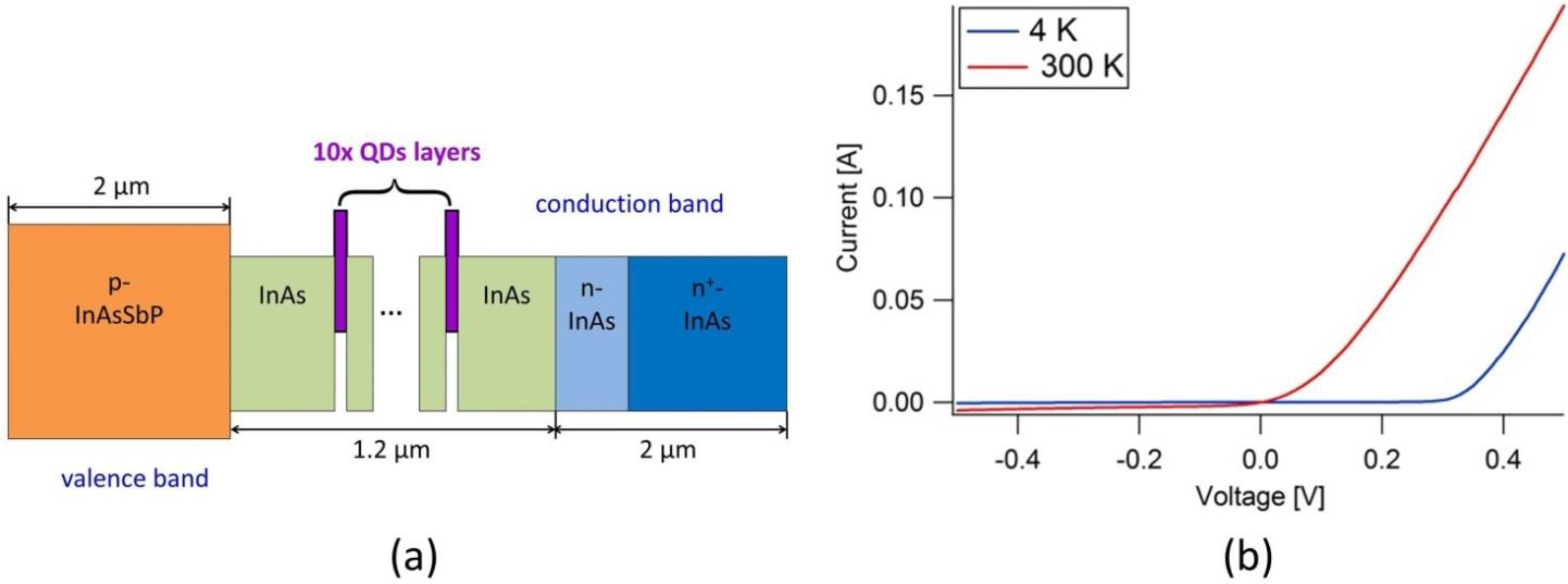
3. Results and Discussion

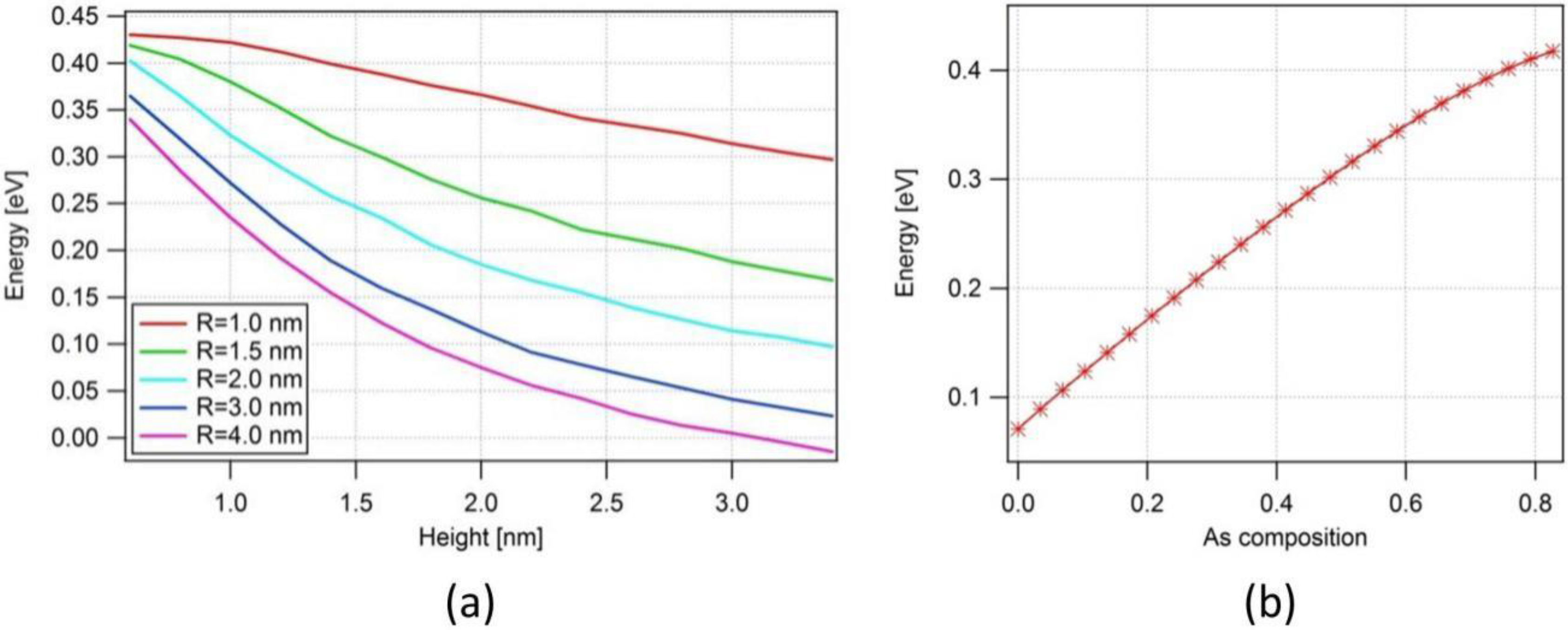
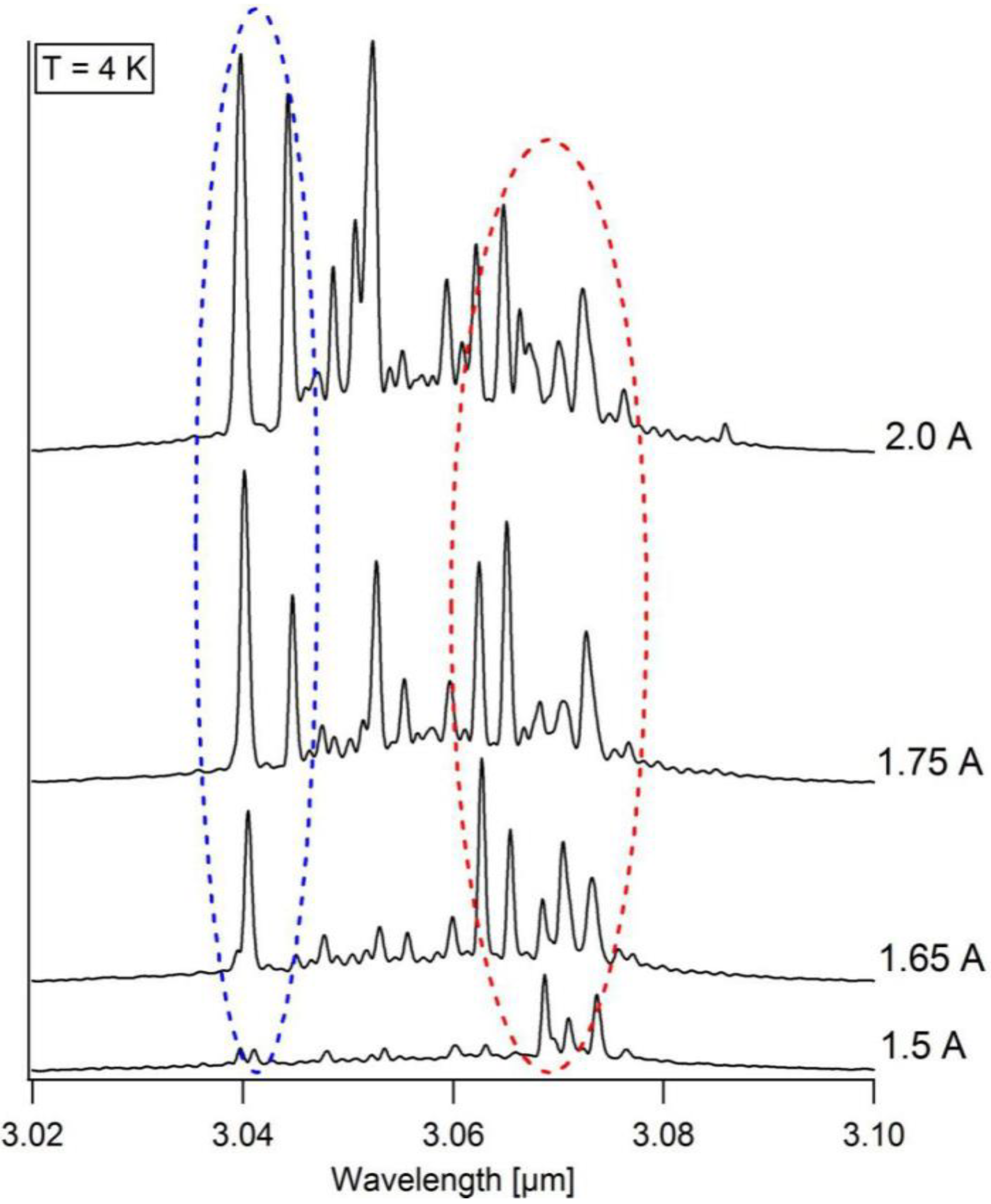
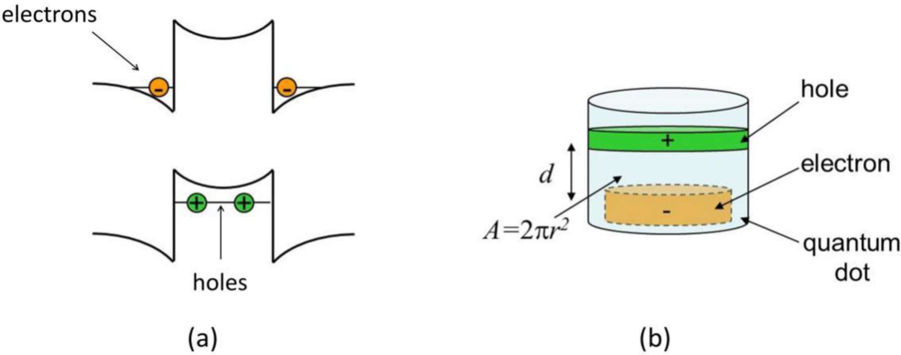
3.1. Gain from InSb QDs

QD laser diodes with different cavity lengths were tested in pulsed mode (100 ns pulse width, 2 kHz repetition rate) from 4 K to 120 K. The threshold current density (Jth) increased from 1.59 kAcm−2 to 4.68 kAcm−2 as the cavity length was reduced from 1.17 mm to 0.33 mm. Using the same method as for QW lasers [12], the gain of our InSb QD lasers was estimated from the relation between Jth and different laser cavity lengths L, using:
J t h = n w J t r η i e x p ( α i + 1 L l n ( 1 R ) n w Γ w G 0 )
where nw is the number of QD layers, Jtr is the transparency current density per layer, ηi is the internal quantum efficiency, αi is the waveguide loss, R is the reflection coefficient of the end facet, ΓwG0 is the modal gain in which Γw is the optical confinement factor per layer and G0 is the material gain coefficient. By making a linear fit between ln (Jth) and 1/L, the modal gain can be extracted.
Figure 2. Threshold current density (Jth) vs. reciprocal cavity length (1/L) of the laser diodes at 4 K. The red line shows the linear fit between ln(Jth) and 1/L.
Photonics 02 00414 g002
From Figure 2, the modal gain of the QD laser was estimated to be ~29 cm−1, (i.e., 2.9 cm−1 per QD layer on average). This value is lower than typical (InAs) type I QDs emitting in the near-infrared range which is in the order of 10 cm−1 [13,14], but is close to that of type II QWs emitting at a similar wavelength [12]. The relatively lower modal gain from type II structures is closely related to the large spatial separation between electrons and holes compared with type I structures, which results in a much smaller electron-hole wave function overlap.
Figure 3. (a) Calculated transition energy of InSb QD as a function of the QD height for different radius (R) values at 4 K. (b) Calculated transition energy of InAsxSb1–x QD as a function of As composition at 4 K, where the QD size is fixed at 3 nm base radius and 2 nm height.
Photonics 02 00414 g003
From previous reports [7,8,9,15], the peak emission wavelength of such InSb QDs typically falls between 3.2 and 3.8 µm at low temperatures, corresponding to transition energies in the range 0.326–0.388 eV. The dependence of transition energies of pure InSb QD on the radius and height of the QDs at 4 K were evaluated using three-dimensional single band Schrödinger calculations in COMSOL multiphysics. The results are plotted in Figure 3a, where the transition energy exhibits a strong dependence on the QD size. For example, with a fixed radius of 2 nm, a 0.5 nm change in QD height (from 1.5 nm to 2 nm) resulted in about 70 meV difference in transition energy. Although the COMSOL calculation is a much simpler estimation than the k.p calculations, the values obtained here are in fact in good agreement with the results from 6 × 6 k.p calculations [16]. Assuming the QD was composed of pure InSb, it was found from both k.p modeling in [16] and COMSOL calculation from Figure 3a that, to achieve typical transition energy of 0.35 eV, the QD height needed to be about 1.0 nm and radius 1.25–1.5 nm. However, high resolution microscopic images reported in [17] revealed that the QDs could possibly be much larger in size (~3 nm base radius and ~2.5 nm in height). The most probable reason for this disagreement is that instead of pure InSb, the QDs may contain a large proportion of As. By fixing the QD size according to the microscopic image in [17], the transition energy dependence on the composition of As was also calculated by the same method in COMSOL and plotted in Figure 3b. To obtain the 0.35 eV transition energy, the QD composition should be close to InAs0.6Sb0.4. It needs to be stressed that one image cannot represent all of the QDs in the structure and it is most likely that there are deviations in both QD size and composition. Thus, both QDs with pure InSb in an extremely small size or larger QDs with more As in the composition can exist in the same sample.
In the In(As)Sb QDs, holes are the only confined carriers, while electrons can move freely in the InAs matrix. Both COMSOL simulations and 6 × 6 k.p calculations [16] confirm that the ground heavy hole (GHH) state was the only confined energy state within QDs of base radius 1.25–3 nm. For both pure InSb QDs (~1.25 nm) and larger InAs0.6Sb0.4 QDs (~3 nm), the electron-hole wave function overlap lies within the range 35%–40% (using both simulation methods), which is lower than in type I QDs and W-structures [18,19]. However, due to the high QD density, an exceptionally high material gain of ~20 × 104 cm−1 can be estimated for our type II QD, which is in the same range as for type I QDs [13]. Despite the smaller electron-hole wave function overlap, these type II QDs can serve as an efficient gain medium for mid-infrared laser diodes.
The laser diodes emitted between 3.02–3.11 µm and the details of the laser spectrum can be revealed by using high resolution Fourier transform infrared (FTIR) spectroscopy. The measured spectra of one laser diode at 4 K with different drive currents are plotted in Figure 4. The relatively broad overall spectra are probably caused by the size distribution of QDs. Two representative groups of modes are circled in this figure. At lower current injection, the longer wavelengths modes (circled in red) appeared first. With higher current injection, the shorter wavelengths modes (circle in blue) became stronger. This means the longer wavelength modes reach threshold first, associated with coherent emission from the larger QDs. This is also consistent with the transfer of holes between adjacent QDs by tunneling or thermal excitation [20] so that QDs with lower GHH states (i.e., emitting at longer wavelengths) become occupied first as current injection is increased.
Figure 4. Multimodal laser spectra measured at 4 K using different pulsed drive currents. Two representative groups of modes are identified and are circled using red and blue dashed lines in the figure.
Photonics 02 00414 g004

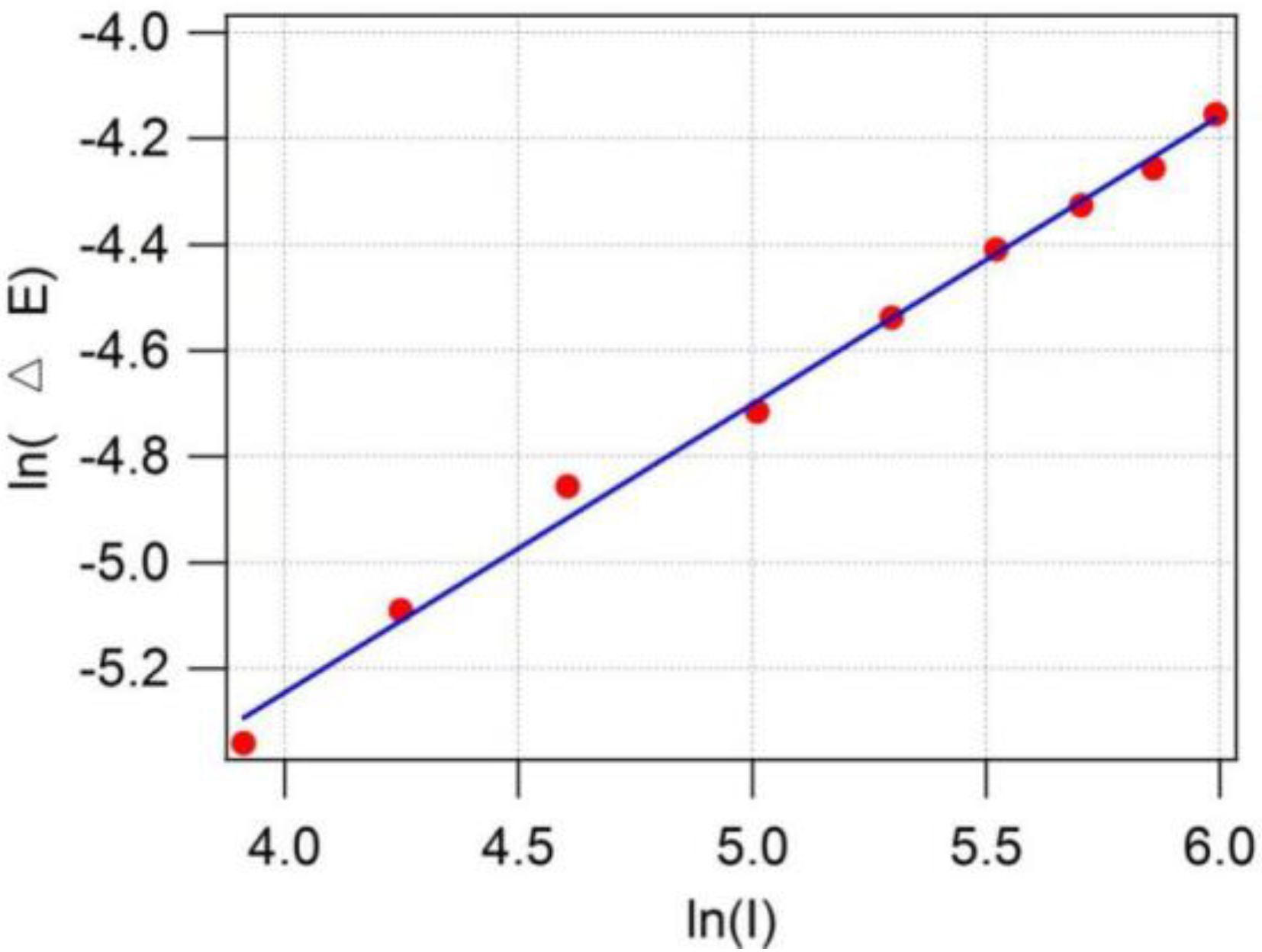
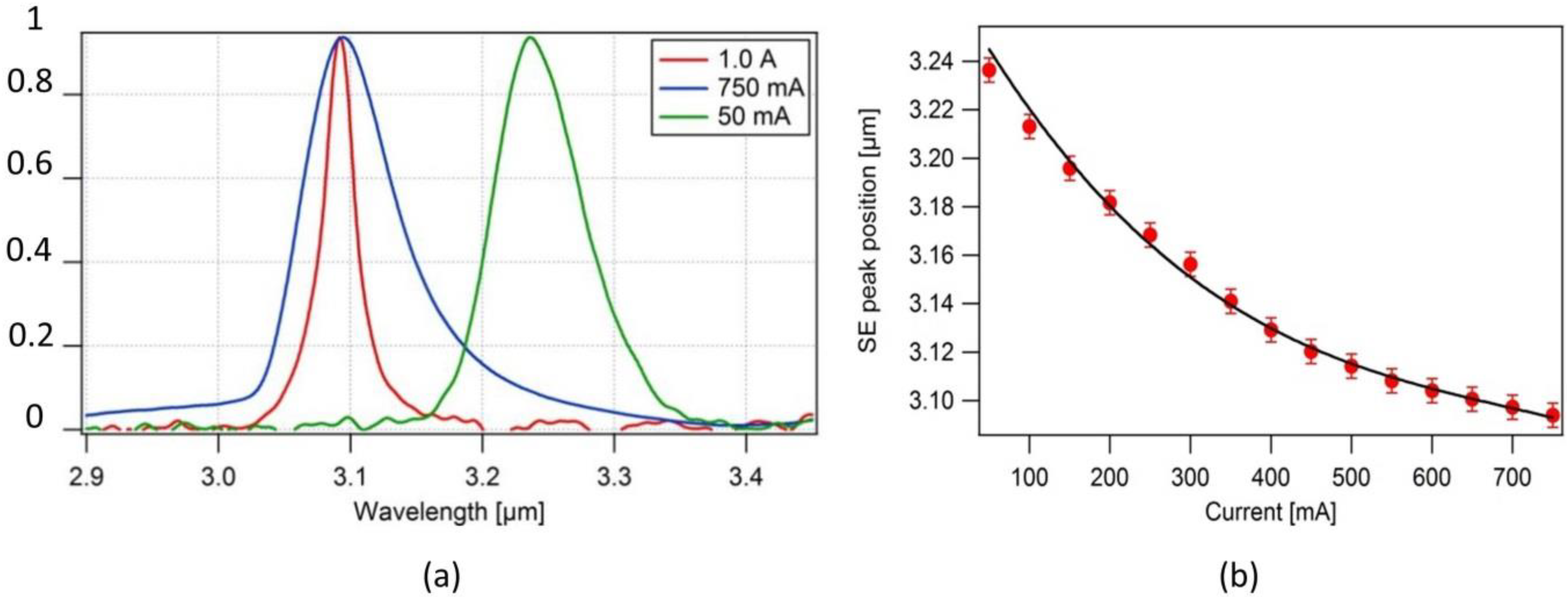
3.2. Spontaneous Emission

The spontaneous electro-luminescence (SE) emission spectra from the laser diodes were measured from the end facet when the injected current was below threshold. An interesting phenomenon was observed that with increasing current injection, there was a large blue shift of the SE peak position. In Figure 5a, the SE peaked at 3.236 µm at 50 mA and moved down to 3.094 µm at 750 mA, corresponding to an energy difference of about 18 meV, but without significant broadening. The above threshold spectrum envelope at 1.0 A is also shown in the low resolution spectra of Figure 5a, where the lasing peak lies very close to the peak of the SE spectrum at 750 mA.
Figure 5. (a) Comparison of the sub-threshold emission spectrum at 50 mA current injection (green curve) and at 750 mA current injection (blue curve) with the laser spectrum envelope just above threshold at 1.0 A current injection (red curve). The peak intensities of the three spectra have been normalized. (b) Below threshold spontaneous emission peak wavelength shift with increasing current from a laser diode measured at 4 K. The threshold current of this laser Ith = 950 mA.
Photonics 02 00414 g005
The SE peak position dependence on the injected current is shown in Figure 5b. In the lower current range the rate of the SE peak shift is greater than in the higher current range. Since there is only one quantized heavy hole state in our QDs, one possible reason to explain the SE peak shift is the band-bending effect caused by the electric field in type II structures. When the holes occupy the QDs, the electrons can be attracted closer to them, causing the conduction band to bend into a triangular shape, as illustrated in Figure 6a. Quantized electron states may occur in the triangular potential, resulting in higher recombination energy. Blue shifts caused by band-bending have already been reported from other kinds of type II QWs [21] and QDs [22]. The relation between the injected current and wavelength shift can be written as [21]:
Δ E B I 1 / 3
where ΔEB is the transition energy shift caused by band-bending, and I is the injected current.
Another possible reason that can cause a blue shift of the SE peak is the charging of QDs. In type II structures, since electrons and holes are spatially separated, the repulsive Coulomb force between carriers of the same type (the injected holes in our case) is much greater than the attractive Coulomb force between electrons and holes [23,24]. The strong interaction between the two holes in GHH state inside the QD can decrease the hole confinement energy, resulting in a blue shift of the SE peak. A single QD can be modelled as a cylindrical capacitor as sketched in Figure 6b. The relation between the transition energy shift arising from this charging effect and injected current can be obtained as:
Δ E C I 1 / 2
where ΔEC is the transition energy shift caused by charging, and I is the injected current.
Figure 6. (a) Illustration of the band-bending effects caused by the electric field in type II nanostructures. (b) Illustration of the simple capacitor model for a QD associated with charging effects.
Photonics 02 00414 g006
Comparing Equations (2) and (3), it is evident that the energy shifts caused by these two mechanisms have different dependence on the injected current. A logarithmic plot of the measured SE peak shift against the current is shown in Figure 7. The slope of the linear fit (blue line) in this plot was 0.53, which confirms that the QD charging effect is responsible for the blue shift of the SE peak.
Figure 7. Logarithmic plot of the SE peak shift (ΔE) at different injected currents (I). The blue line is a linear fit between ln(ΔE) and ln(I). The slope = 0.53.
Photonics 02 00414 g007

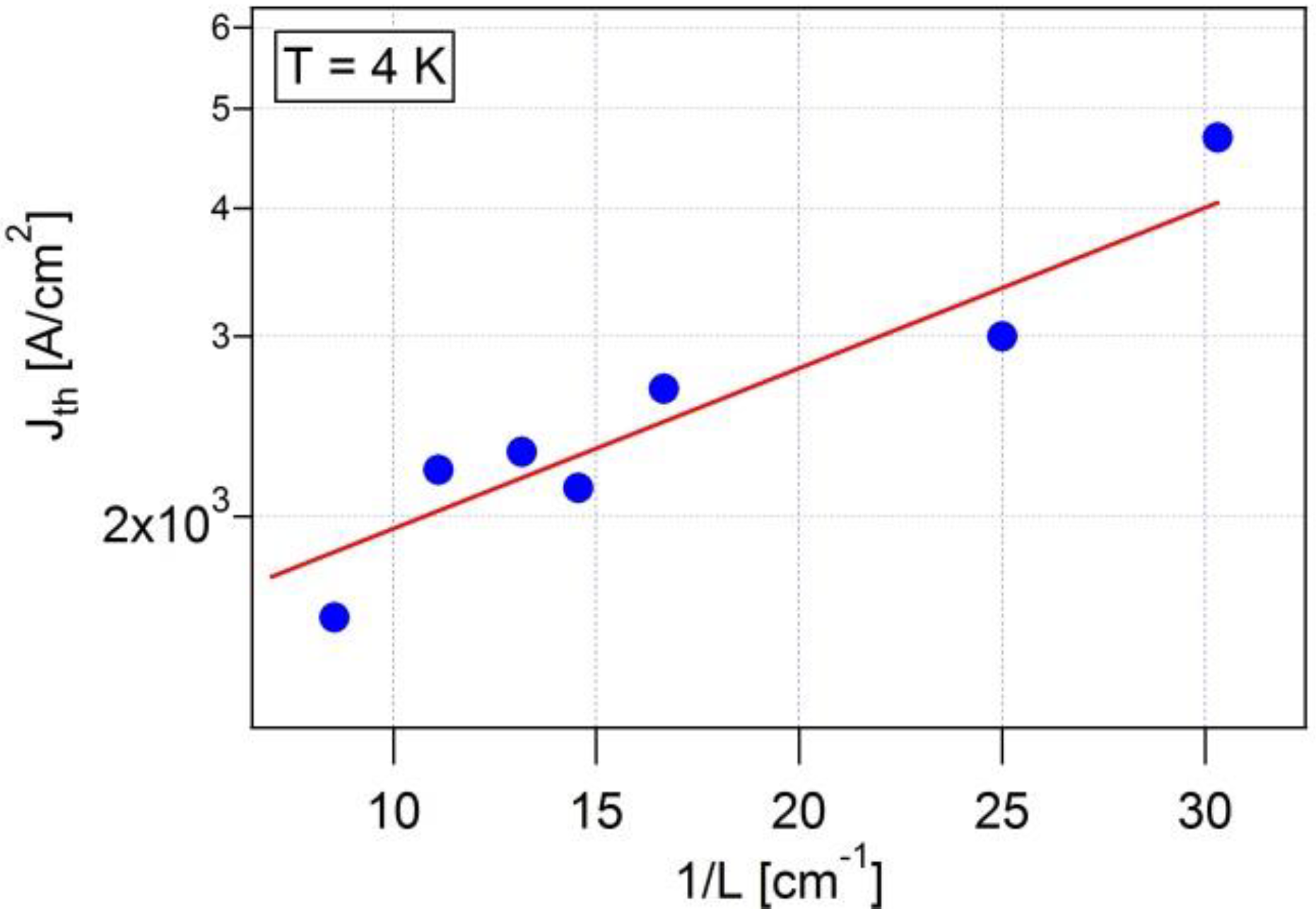
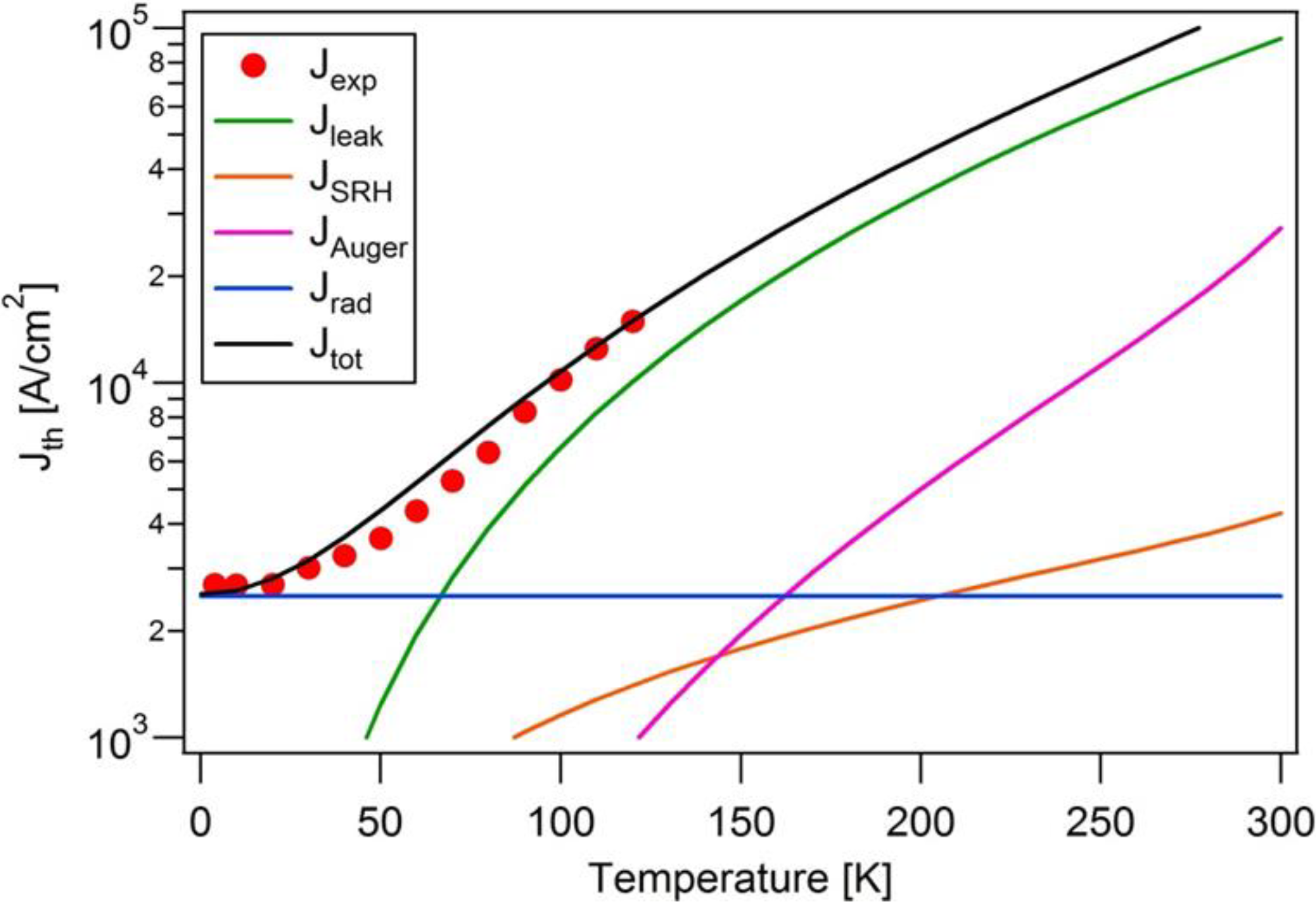
3.3. Non-Radiative current

With increasing temperature, the threshold current density Jth of the laser diodes increased rapidly. However, compared to previous reports the measured maximum working temperature (Tmax) was improved from 60 K to 120 K, because of improved waveguide design and cladding layer material quality. The relationship between Jth and temperature was plotted in Figure 8, where the characteristic temperature, T0 was estimated to be 101 K when the temperature was below 50 K. For the temperature range between 50 K and 120 K, the value of T0 dropped to 48 K. Possible contributions towards the increase of Jth and decrease of T0 include: the leakage current, Auger recombination and Shockley-Read-Hall (SRH) recombination. The total current density Jtot can be expressed as [25]:
J t o t ( T ) = J l e a k + J r a d + J S H R + J A u g e r = J l e a k + J r a d + e d e f f ( A n + C n 3 )
where Jleak, Jrad, JSRH and JAuger are the leakage current, radiative current, SRH current and Auger current, respectively. The terms An and Cn3 represent contributions from SRH and Auger recombination, where n is the threshold carrier density and deff is the effective width of the active region. The relation between temperature and Jleak was taken from [26]. In ideal QD lasers, Jrad should be temperature independent [6,27]. The calculated JSRH, JAuger and Jleak were plotted in Figure 8, where we have used representative values of the respective coefficients taken from the literature [26,28]. The Jtot (black curve) was then fitted to the experimental data Jexp by adjusting the constant value of Jrad.
Figure 8. Measured threshold current density (red dots) of the In(As)Sb QD laser at different temperatures. Calculated Jleak (green curve), JSRH (orange curve), JAuger (pink curve), Jrad (blue line) and Jtot (black curve) are also presented.
Photonics 02 00414 g008
It is evident that for T < 40 K, the contributions from all three non-radiative mechanisms were negligible compared with the experimental data (Jexp), thus the high Jth in the low T region can only be attributed to radiative recombination. The Jrad was fixed at 2.5 kA/cm2 to make a reasonable fit between Jtot and Jexp. This plot also implies that Jleak is the dominant non-radiative component above 50 K. In fact, according to this calculation, at 120 K only 17% of the total current contributed towards radiative recombination, while leakage current consumed 67% of the total current. Within Jleak, the hole leakage was the dominating factor, since there was no valence band offset between the waveguide and n-cladding. The threshold current density at 4 K is rather high and requires explanation. According to Figure 8, the main contribution to the threshold current at this temperature is radiative. Because there is a distribution of QD size and composition, only a small fraction of QDs achieve threshold at the same injection level, and a large part of the radiative current is essentially wasted. Figure 4 confirms that QD of different sizes give coherent emission at different injection levels, with the larger QD being the first to reach threshold. We can speculate that only ~1%–10% of the QD are lasing together at each temperature.

4. Conclusions

We investigated the gain and characteristic temperature dependence of type II In(As)Sb/InAs QDs for use in mid-infrared laser diodes. The devices emitted at around 3.1 µm and operated up to 120 K. The transition energy dependences on QD size and composition were calculated. The charging effect in the QDs was identified as the main reason for the blue shift in the spontaneous electro-luminescence. Different non-radiative recombination mechanisms were compared, and it was found that the leakage current was the major factor for the increase of Jth with temperature, though the Jrad needed to obtain lasing threshold was also quite high. In order to improve the Tmax and reduce Jth, the Jleak should be effectively suppressed, probably by inserting a hole blocking layer in the laser structure. The Jrad also needs to be reduced, which can only be achieved by increasing the modal gain of the QDs and carefully controlling the size distribution of the QDs.

Acknowledgments

This work was supported by the European Marie Curie Initial Training Network PROPHET, Grant No. 264687. We are grateful to Min Yin and Jonathan Hayton for the LPE growth of the InAs0.61Sb0.13P0.26 cladding layers.

Author Contributions

Qiandong Zhuang and Qi Lu did the MBE growth of the laser structure. Qi Lu fabricated the laser diodes, characterized the devices, analyzed the performances and wrote the manuscript. Anthony Krier supervised the work and modified the article.

Conflict of Interest

The authors declare no conflict of interest.

References

  1. Krier, A.; Yin, M.; Smirnov, V.; Batty, P.; Carrington, P.J.; Solovev, V.; Sherstnev, V. The development of room temperature LEDs and lasers for the mid-infrared spectral range. Phys. Status Solidi(a) 2008, 205, 129–143. [Google Scholar] [CrossRef]
  2. Yin, Z.; Tang, X. A review of energy bandgap engineering in III–V semiconductor alloys for mid-infrared laser applications. Solid. State. Electron. 2007, 51, 6–15. [Google Scholar] [CrossRef]
  3. Range, W.; Hosoda, T.; Kipshidze, G.; Tsvid, G.; Shterengas, L.; Belenky, G. Type-I GaSb-based laser diodes operating in 3.1- to 3.3-um wavelength range. IEEE Photon. Technol. Lett. 2010, 22, 718–720. [Google Scholar] [CrossRef]
  4. Yao, Y.; Hoffman, A.J.; Gmachl, C.F. Mid-infrared quantum cascade lasers. Nat. Photonics 2012, 6, 432–439. [Google Scholar] [CrossRef]
  5. Vurgaftman, I.; Bewley, W.W.; Canedy, C.L.; Kim, C.S.; Kim, M.; Lindle, J.R.; Merritt, C.D.; Abell, J.; Meyer, J.R. Mid-IR type-II interband cascade lasers. IEEE J. Sel. Top. Quant. Electron. 2011, 17, 1435–1444. [Google Scholar] [CrossRef]
  6. Coleman, J.J.; Young, J.D.; Garg, A. Semiconductor quantum dot lasers: a tutorial. Semicond. Sci. Technol. 2011, 29, 499–510. [Google Scholar]
  7. Solov’ev, V.A.; Carrington, P.; Zhuang, Q.; Lai, K.T.; Haywood, S.K.; Ivanov, S.V.; Krier, A. InSb/InAs nanostructures grown by molecular beam epitaxy using Sb2 and As2 fluxes. In Proceedings of the 13th International Conference on Narrow Gap Semiconductors 2007, Guildford, UK, 8–12 July 2007; pp. 129–131.
  8. Carrington, P.J.; Solov’ev, V.A.; Zhuang, Q.; Krier, A.; Ivanov, S.V. Room temperature midinfrared electroluminescence from InSb/InAs quantum dot light emitting diodes. Appl. Phys. Lett. 2008, 93, 091101. [Google Scholar] [CrossRef]
  9. Carrington, P.J.; Solov’ev, V.A.; Zhuang, Q.; Ivanov, S.V.; Krier, A. InSb quantum dot LEDs grown by molecular beam epitaxy for mid-infrared applications. Microelectron. J. 2009, 40, 469–472. [Google Scholar] [CrossRef]
  10. Solov’ev, V.A.; Sedova, I.V.; Lyublinskaya, O.G.; Semenov, A.N.; Mel’tser, B.Y.; Sorokin, S.V.; Terent, Y.V.; Ivanov, S.V. Midinfrared injection-pumped laser based on a III–V/II–VI hybrid heterostructure with submonolayer InSb insets. Tech. Phys. Lett. 2005, 31, 235–237. [Google Scholar] [CrossRef]
  11. Yamaguchi, K.; Yujobo, K.; Kaizu, T. Stranski-Krastanov growth of InAs quantum dots with narrow size distribution. Jpn. J. Appl. Phys. 2000, 39, 1245–1248. [Google Scholar] [CrossRef]
  12. Wilk, A.; El Gazouli, M.; El Skouri, M.; Christol, P.; Grech, P. Type-II InAsSb/InAs strained quantum-well laser diodes emitting at 3.5 µm. Appl. Phys. Lett. 2000, 77, 2298. [Google Scholar] [CrossRef]
  13. Kirstaedter, N.; Schmidt, O.G.; Ledentsov, N.N.; Bimberg, D.; Ustinov, V.M.; Egorov, A.Y.; Zhukov, A.E.; Maximov, M.V.; Kop’ev, P.S.; Alferov, Z.I. Gain and differential gain of single layer InAs/GaAs quantum dot injection lasers. Appl. Phys. Lett. 1996, 69, 1226. [Google Scholar] [CrossRef]
  14. Lelarge, F.; Rousseau, B.; Dagens, B.; Poingt, F.; Pommereau, F.; Accard, A. Room temperature continuous-wave operation of buried ridge stripe lasers using InAs-InP (100) quantum dots as active core. IEEE Photon. Technol. Lett. 2005, 17, 1369–1371. [Google Scholar] [CrossRef]
  15. Lu, Q.; Zhuang, Q.; Marshall, A.; Kesaria, M.; Beanland, R.; Krier, A. InSb quantum dots for the mid-infrared spectral range grown on GaAs substrates using metamorphic InAs buffer layers. Semicond. Sci. Technol. 2014, 29, 075011. [Google Scholar] [CrossRef]
  16. Yeap, G.H.; Rybchenko, S.I.; Itskevich, I.E.; Haywood, S.K. Type-II InAsxSb1−x/InAs quantum dots for midinfrared applications: Effect of morphology and composition on electronic and optical properties. Phys. Rev. B 2009, 79, 075305. [Google Scholar] [CrossRef]
  17. Lu, Q.; Zhuang, Q.; Hayton, J.; Yin, M.; Krier, A. Gain and tuning characteristics of mid-infrared InSb quantum dot diode lasers. Appl. Phys. Lett. 2014, 105, 031115. [Google Scholar] [CrossRef]
  18. Joullié, A.; Christol, P. GaSb-based mid-infrared 2–5 μm laser diodes. CR Phys. 2003, 4, 621–637. [Google Scholar] [CrossRef]
  19. Janssens, K.L.; Partoens, B.; Peeters, F.M. Magnetoexcitons in planar type-II quantum dots in perpendicular magnetic field. Phys. Rev. B 2001, 64, 155324. [Google Scholar] [CrossRef]
  20. Lyublinskaya, O.G.; Solov’ev, V.A.; Semenov, A.N.; Meltser, B.Y.; Terent’ev, Y.V.; Prokopova, L.A.; Toropov, A.A.; Sitnikova, A.A.; Rykhova, O.V.; Ivanov, S.V.; et al. Temperature-dependent photoluminescence from type-II InSb/InAs quantum dots. J. Appl. Phys. 2006, 99, 093517. [Google Scholar] [CrossRef]
  21. Ledentsov, N.N.; Bohrer, J.; Beer, M.; Heinrichsdorff, F.; Grundmann, M.; Bimberg, D. Radiative states in type-II GaSb/GaAs quantum wells. Phys. Rev. B 1995, 52, 58–66. [Google Scholar] [CrossRef]
  22. Sun, C.; Wang, G.; Bowers, J.E.; Brar, B.; Blank, H. Optical investigations of the dynamic behavior of GaSb/GaAs quantum dots. Appl. Phys. Lett. 1996, 68, 1543–1545. [Google Scholar] [CrossRef]
  23. Gradkowski, K.; Pavarelli, N.; Ochalski, T.J.; Williams, D.P.; Tatebayashi, J.; Huyet, G.; O’Reilly, E.P.; Huffaker, D.L. Complex emission dynamics of type-II GaSb/GaAs quantum dots. Appl. Phys. Lett. 2009, 95, 061102. [Google Scholar] [CrossRef]
  24. Tatebayashi, J.; Khoshakhlagh, A.; Huang, S.H.; Balakrishnan, G.; Dawson, L.R.; Huffaker, D.L.; Bussian, D.A.; Htoon, H.; Klimov, V. Lasing characteristics of GaSb/GaAs self-assembled quantum dots embedded in an InGaAs quantum well. Appl. Phys. Lett. 2007, 90, 261115. [Google Scholar] [CrossRef]
  25. Choulis, S.A.; Andreev, A.; Merrick, M.; Adams, A.R.; Murdin, B.N.; Krier, A.; Sherstnev, V.V. High-pressure measurements of mid-infrared electroluminescence from InAs light-emitting diodes at 3.3 μm. Appl. Phys. Lett. 2003, 82, 1149. [Google Scholar] [CrossRef] [Green Version]
  26. Mani, H. Realization and study of a double hetero-structure InAsSb/InAsSbP laser emitting beyond 3 micrometer. Ph.D. thesis, Université des sciences et techniques de Montpellier 2, Montpellier, France, 1989. [Google Scholar]
  27. Fathpour, S.; Mi, Z.; Bhattacharya, P.; Kovsh, A.R.; Mikhrin, S.S.; Krestnikov, I.L.; Kozhukhov, A.V.; Ledentsov, N.N. The role of Auger recombination in the temperature-dependent output characteristics (T0 = ∞) of p-doped 1.3 μm quantum dot lasers. Appl. Phys. Lett. 2004, 85, 5164–5166. [Google Scholar] [CrossRef]
  28. Meyer, J.R.; Felix, C.L.; Bewley, W.W.; Vurgaftman, I.; Aifer, E.H.; Olafsen, L.J.; Lindle, J.R.; Hoffman, C.A.; Yang, M.-J.; Bennett, B.R.; et al. Auger coefficients in type-II InAs/Ga1-xInxSb quantum wells. Appl. Phys. Lett. 1998, 73, 2857–2859. [Google Scholar] [CrossRef]

