1. Introduction
Low-dimensional materials, leveraging quantum confinement effects, surface-dominated behaviors, and atomic-level tunability, have systematically outperformed conventional bulk materials in infrared detection. Tellurium (Te), as a one-dimensional van der Waals material, features a crystal structure composed of helical monatomic chains stacked along the c-axis, with strong covalent bonding within each chain and weak van der Waals interactions between chains [
1,
2,
3]. This unique helical architecture enables a room-temperature carrier mobility of up to 1000 cm
2/V·s [
4], significantly surpassing that of conventional two-dimensional semiconductors such as MoS
2 and MoSe
2 [
5,
6,
7]. Such exceptional charge transport properties dramatically enhance the response speed and signal transmission efficiency of infrared photodetectors, serving as a fundamental enabler for high-speed, high-sensitivity infrared detection [
8,
9,
10,
11,
12,
13]. By tuning the bandgap within the range of 0.35–1.04 eV, Te-based photodetectors enable continuous spectral response across the visible-to-mid-infrared regime, overcoming the inherent spectral limitation of conventional materials that are confined to single-wavelength detection. The anisotropy of the material in both optical and electrical aspects has also been investigated [
14,
15], which has significantly facilitated its application in polarization-sensitive detection [
16,
17,
18]. With the rapid advancement of material synthesis and processing technologies, research on Te has transitioned from laboratory-scale single-crystal micro- and nanostructures to wafer-scale [
19,
20], flexible [
21,
22], and CMOS-compatible thin-film platforms [
23,
24].
To further enhance the performance of these devices based on low-dimensional materials, substantial efforts have been directed toward two primary strategies: the construction of van der Waals heterostructures [
25,
26,
27] and the integration of metasurfaces [
28,
29,
30]. The latter approach not only leverages resonant geometries to amplify optical absorption within targeted spectral bands, thereby significantly boosting photocurrent response, but also enables precise modulation of the local electromagnetic field–detector coupling [
31,
32,
33]. This tunable interaction empowers the detector to simultaneously sense multidimensional optical information, including polarization, phase, wavelength, angle of incidence, and orbital angular momentum [
34,
35,
36]. Consequently, the fusion of metasurfaces with photodetectors has emerged as a pivotal frontier in optoelectronics, catalyzing a wave of innovative designs that transcend conventional detection paradigms. The inherently limited optical absorption of graphene severely constrains its efficacy in photodetector applications. To address this limitation, Attarabad et al. developed a graphene-based photodetector integrated with a plasmonic metasurface composed of omega-shaped optical nanoantennas [
37]. This architecture dramatically enhances light–matter coupling between incident radiation and the graphene active layer, resulting in a substantial boost in photonic absorption. By precisely tuning the geometric parameters of the metasurface, a broadband and tunable absorption peak was engineered at the 1550 nm telecommunications wavelength, elevating the graphene absorption to 66%, a near-threefold improvement over conventional graphene-only devices. In 2022, Nikola developed a colloidal quantum dot (QD)-based metasurface-enhanced photodetector that achieves a high responsivity of up to 8000 A/W across the 1550 nm wavelength range, while maintaining full compatibility with standard CMOS circuitry [
38]. The exceptional responsivity is attributed to the metasurface’s ability to enhance optical absorption by a factor of ten compared to conventional QD films of identical thickness, thereby enabling substantial optical gain. This design simultaneously overcomes the intrinsic absorption limitations of ultrathin QD layers and enables high-performance infrared detection in a monolithically integrable platform. The integration of nanoscale metasurfaces with photodetectors has substantially enhanced the performance of the devices, notably increased the photoresponsivity, broadened the spectral bandwidth, and enabled multifunctional detection.
In this study, the geometric parameters of a dual-C open-ring metallic metasurface were systematically investigated using the finite-difference time-domain (FDTD) method to regulate the light absorption characteristics at 4 μm and 6 μm, thereby optimizing the device performance model. Large-area, high-quality Te thin films were fabricated via magnetron sputtering followed by annealing, enabling the construction of a metasurface-enhanced Te-based mid-infrared photodetector. Ultimately, the metasurface-enhanced Te-based device achieved responsivities of 10.5 A/W and 13.7 A/W at 4 μm and 6 μm, respectively, representing enhancements of 3.6-fold and 3-fold compared to the initial Te thin-film device.
3. Results and Discussion
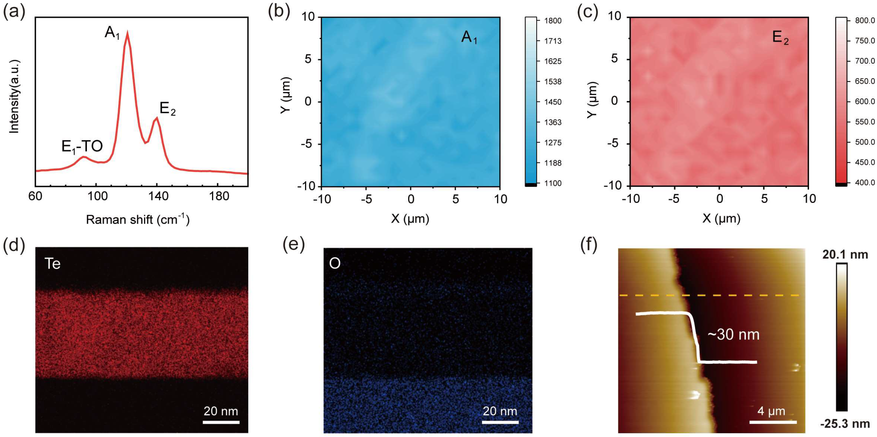
Te films were fabricated by magnetron sputtering followed by an annealing treatment. Raman spectroscopy was utilized to evaluate the crystalline quality and compositional uniformity of as-prepared films. As illustrated in
Figure 1a, the Te film exhibits three dominant Raman peaks at 91.5, 120.6, and 140.1 cm
−1, which correspond to the intra-chain shear bending (E
1), inter-chain longitudinal expansion (A
1), and intra-chain symmetric stretch (E
2), respectively [
39]. The Raman mapping results presented in
Figure 1b,c demonstrate spatially uniform intensity distribution of the A
1 and E
2 modes across the 20 × 20 μm
2 scan, thus verifying the excellent structural homogeneity of the Te thin film.
As shown in
Figure 1d,e, energy-dispersive spectrometer (EDS) analysis of the cross-section prepared by focused ion beam (FIB) reveals a homogeneous distribution of Te with negligible oxygen contamination. This confirms that the magnetron-sputtered Te film exhibits both excellent compositional uniformity and ultra-high purity. Atomic force microscopy (AFM) imaging (
Figure 1f) confirms that the Te film has a uniform thickness of 30 nm with minimal topographical variation, verifying a flat, homogeneous surface. The scanning electron microscopy (SEM) image presented in
Figure S1 demonstrates a uniform surface morphology of the Te film. Meanwhile, high-resolution transmission electron microscopy (HRTEM) characterization confirms a lattice fringe spacing of 0.38 nm, which corresponds to the (100) crystal plane of Te [
40]. Collectively, these structural and morphological characterizations conclusively confirm the successful synthesis of highly crystalline, phase-pure Te thin films.
For metallic nanostructures, tuning the surface plasmon resonance (SPR) wavelength is a result of the synergistic interplay of multiple physical parameters. The enhancement of the local electromagnetic field is heavily dependent on the geometric configuration of the nano-units, such as their size distribution, shape characteristics, and crystal-plane orientation, as well as the topological arrangement of the array and the coupling distance between adjacent units [
41,
42]. Subsequently, the key structural parameters are investigated to optimize the optical absorption characteristics of the designed plasmonic structure.
Figure S2 illustrates the schematic configuration of the single-period unit cell in the simulation software (Ansys Lumerical 2020 R2.4). The device structure, from top to bottom, comprises a Au metasurface, a Te film, an Al
2O
3 layer, a Au back reflector, a SiO
2 insulating layer, and a Si substrate. The 20 nm thick Au back reflector recouples unabsorbed incident light back into the semiconductor active region, extending the effective optical path length within the absorption layer. This not only boosts the system’s incident light absorption efficiency but also enables broadband absorption. With its high resistivity and dielectric strength, Al
2O
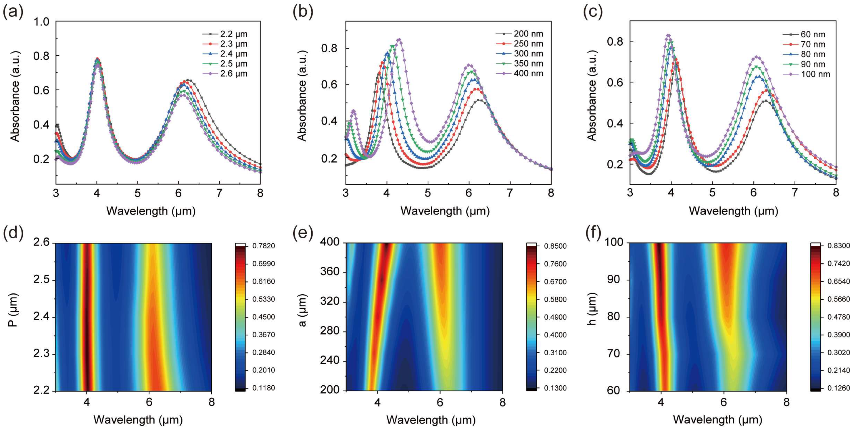
3 acts as an ideal insulating spacer layer. It serves dual roles: not only as an isolation layer but also as the spacer for the resonant cavity. By precisely tuning the phase relationship between its thickness and the incident wavelength, a standing-wave field distribution is formed within the dielectric layer, confining electromagnetic field energy primarily at the interface of the Te absorption layer. During the simulation, with all other conditions kept constant, the period P was swept from 2.2 to 2.6 μm. The corresponding absorption spectra of the structure at this time are presented in
Figure 2a. Under the initial condition where P is 2.2 μm, resonant peaks with absorptance values of 0.76 and 0.68 appear at 4.04 μm and 6.22 μm, respectively. As the period P increases to 2.6 μm, the resonant peaks shift to 4.01 μm and 6.06 μm, and the corresponding absorptance values are 0.74 and 0.57, respectively. As depicted in
Figure 2d, increasing P induces only a minor blue shift in the peak near 4 μm, while the absorption intensity remains largely unchanged. In contrast, the peak at 6 μm exhibits a significant blue shift accompanied by a reduction in light absorption intensity. As the lattice period P increases, the near-field coupling between adjacent structural units gradually weakens, which leads to progressive decoupling of the lattice modes and a corresponding blue shift in their intrinsic resonant frequency. Concurrently, the modified lattice diffraction conditions alter the phase-matching condition, triggering modal mismatch, enhanced radiation loss into free space, and a corresponding reduction in optical absorption intensity. In the period- and wavelength-dependent spectral response, the full width at half maximum of the short-wavelength resonance peak remains largely unchanged as the lattice period P increases, whereas that of the long-wavelength resonance peak progressively narrows. The quality factor (Q) of the short-wavelength peak is predominantly determined by the intrinsic and non-radiative losses inherent to the metallic material. Owing to the highly localized nature of the localized SPR mode, electromagnetic coupling between adjacent nanostructures remains weak. As a result, the radiative loss and hence the total damping rate exhibit minimal variation with P. Even when P increases, the localized mode’s near-field decays exponentially with interparticle distance, but the coupling strength remains negligible compared to intrinsic losses. Consequently, radiative loss exhibits minimal variation with lattice period P, resulting in stable linewidth behavior. In contrast, the long-wavelength resonance arises from the interplay of lattice-mode excitation and Fano interference, making its Q factor strongly sensitive to P. Here, the lattice mode involves coherent radiative coupling among periodic scatterers. As P increases, the near-field coupling between neighboring unit cells diminishes, which reduces the radiative damping of the lattice mode. This decrease in radiative loss leads to a higher Q factor and corresponding spectral narrowing. More specifically, for a smaller P, strong near-field interactions enhance radiative damping, broadening the Fano resonance and lowering Q. As P grows, the system approaches the weak-coupling regime, where the lattice mode becomes less lossy, and the Q factor increases approximately as Q~P
α (with α > 0 depending on the exact geometry). This trend is further corroborated by coupled-mode theory: the decay rate due to radiation scales with the interparticle coupling strength, which decays with increasing period. Consequently, the long-wavelength peak’s FWHM narrows monotonically with P, in clear contrast to the short-wavelength case.
The linewidth (
) of metallic metasurfaces is a critical factor governing LSPR mode. Narrow-linewidth structures, such as nanogaps or subwavelength metallic wires, exhibit enhanced LSPR excitation and stronger optical field confinement, thereby significantly boosting light absorption efficiency [
43]. To systematically investigate how linewidth
affects the absorption performance of the metasurface structure, all other geometric and material parameters were kept constant while
was varied parametrically from 200 nm to 400 nm. The corresponding absorption spectra are shown in
Figure 2b. As
increases from 200 nm to 400 nm, the short-wavelength resonance peak red-shifts from 3.79 μm to 4.30 μm, and peak absorption increases from 0.66 to 0.85 accordingly. Concurrently, the long-wavelength resonance peak blue-shifts from 6.22 μm to 5.98 μm, with peak absorption increasing from 0.52 to 0.70. As depicted in
Figure 2e, increasing the linewidth induces opposing shifts in the resonant peaks of the metal surface plasmon polaritons: The resonance peak at 4 μm red-shifts, while the corresponding light absorption intensity rises. Meanwhile, the resonance peak at 6 μm undergoes a blue shift, accompanied by a reduction in light absorption intensity. The energy dissipation of localized surface plasmons primarily stems from two mechanisms: ohmic losses within the metallic material and radiative losses. As the linewidth increases, the volume of the metallic nanostructure expands, which elevates the probability of collisions between free electrons and both lattice vibrations (phonons) and structural defects, leading to a significant increase in ohmic loss. This enhanced dissipation shortens the lifetime of the LSP resonance, which is experimentally observed as spectral broadening. Moreover, increasing the linewidth moderately strengthens the near-field coupling between adjacent structures, introducing additional radiative damping. As a result, the Q factor decreases, which further promotes the broadening of resonant peaks.
In the device architecture, the thickness of the Al
2O
3 insulating layer dictates the optical path difference within the resonant cavity. Resonance is achieved when the layer thickness satisfies the phase-matching condition relative to the incident light wavelength. This in turn optimizes the interfacial electric field distribution, enhancing interference-induced light absorption within a targeted spectral band.
Figure 2c presents the absorption spectra of the metasurface structures as the thickness h is systematically varied from 60 nm to 100 nm, with all other geometric parameters remaining constant. As h increases, both resonant absorption peaks exhibit a blue shift: The short-wavelength peak transitions from 4.12 μm to 3.95 μm, while the peak absorption coefficient rises from 0.69 to 0.83, indicating enhanced light–matter coupling efficiency under increased layer thickness. Similarly, the long-wavelength peak blue-shifts from 6.30 μm to 6.06 μm, with its corresponding absorption magnitude rising from 0.51 to 0.72. Notably, a thicker Al
2O
3 spacer layer weakens the near-field coupling between the metallic metasurface and the underlying cavity mode, which likely contributes to the observed trade-off between spectral shift and absorption enhancement. Consequently, the long-wavelength resonance peak, which is initially dominated by the lattice resonance mode, undergoes a modal transition to the LSPR mode. This modal shift reduces the equivalent inductance of the metasurface structure and elevates the resonance frequency, ultimately inducing a distinct blue shift in the absorption peak. Moreover, increasing the thickness h of the Al
2O
3 dielectric layer enhances electromagnetic field confinement within the dielectric medium, which suppresses radiative energy leakage into free space and promotes energy dissipation through metallic ohmic loss and dielectric loss, thus improving the overall absorption efficiency. Concurrently, the expanded effective volume of the metal–dielectric hybrid structure elevates the probability of electron–lattice and electron–defect scattering events, intensifying ohmic loss in the metallic components and shortening the plasmon resonance lifetime—a phenomenon evidenced by the broadening of the resonance peaks. Furthermore, a thicker Al
2O
3 layer weakens electromagnetic field localization at the metal surface, attenuating near-field coupling between adjacent meta-atoms; this results in spatial delocalization of the field distribution, reduced localized energy concentration, and additional spectral broadening of the absorption peaks.
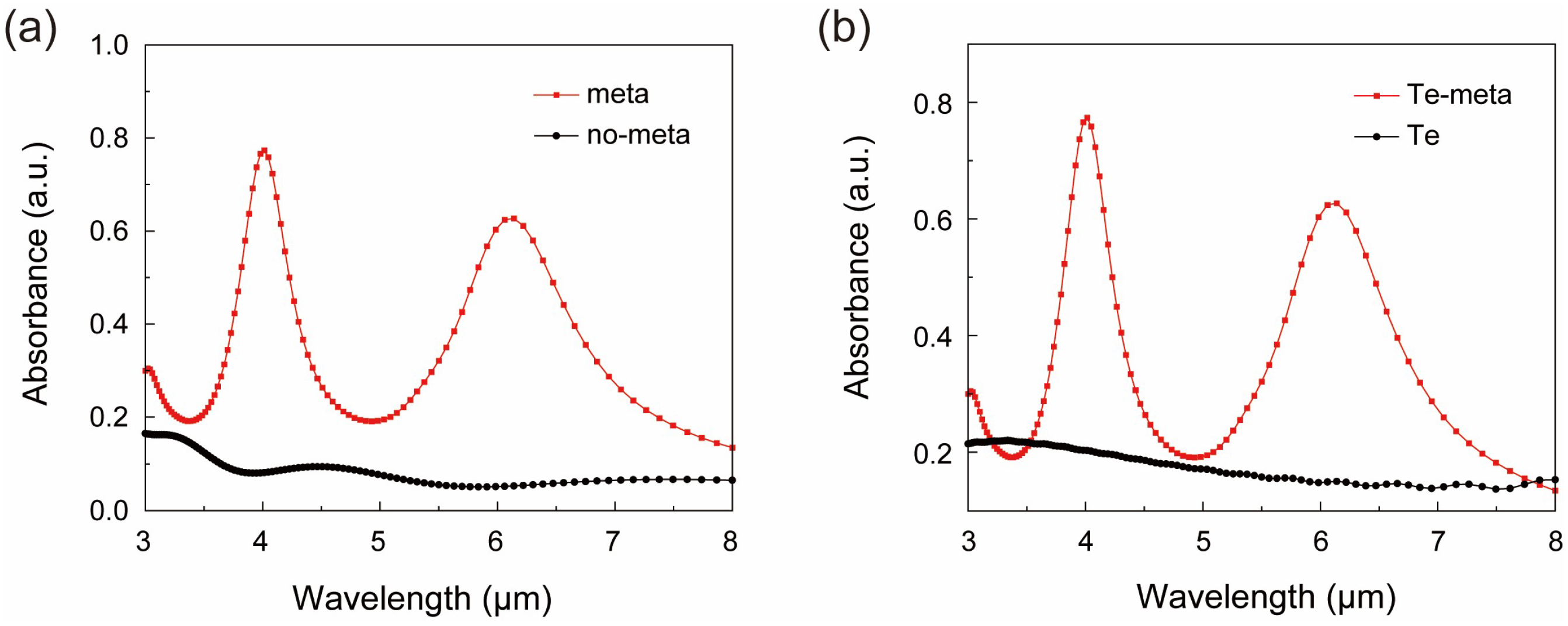
A comprehensive parametric sweep was conducted to identify the optimal resonant wavelengths, where the impacts of all structural parameters on resonance positions and corresponding absorption intensities were systematically evaluated. These wavelengths correspond to near-unity absorption, as evidenced by the spectral response in
Figure 3. Following the implementation of the tailored metasurface structure, the absorption spectrum exhibited distinct and significant alterations, as depicted in
Figure 3a. The absorption peaks are attributed to the excitation of LSPR induced by the periodic arrangement of the metasurface structure. When the incident wavelength matches the resonant wavelength of the structure, the incident light field is strongly localized and amplified, thereby triggering pronounced resonant absorption at these specific wavelengths. The absorption valleys arise from the suppression of Bragg scattering. When the wavelength of incident light approaches the Bragg wavelength matching the structure period, the light undergoes scattering or reflection, giving rise to distinct valleys in the absorption spectrum. In contrast, the metallic double-C open-ring structure, which supports LSPR, exhibits two prominent absorption peaks. The short-wavelength resonant peak is centered at 4 μm with an absorption rate of 0.79, while the long-wavelength resonant peak is located at 6 μm with an absorption rate of 0.65. The light absorption performance of the structure has been significantly enhanced, with absorption intensities at both 4 μm and 6 μm increasing by approximately 8-fold compared to the reference structure. Additionally, we investigated the variation in light absorption performance of the standalone Te film, as depicted in
Figure 3b. Compared with this baseline, our designed metasurface-enhanced structure boosts the light absorption of the Te film by a factor of four at both 4 μm and 6 μm wavelengths, highlighting the significant plasmonic enhancement effect of the metasurface configuration.
Next, we analyze the electric field distribution characteristics at wavelengths of 4 μm and 6 μm, both with and without the metasurface structure.
Figure S4a,b present the electric field intensity distribution in the xy-plane on the Te surface without the metasurface structure. The overall field intensity remains extremely low, exhibiting negligible spatial variation and no observable local field enhancement.
Figure S4c displays the xy-plane electric field distribution at the interface between the Te film and the metallic metasurface under 4 μm wavelength illumination. The doubly symmetric configuration of the paired C-shaped open-ring resonators enables the excitation of well-defined electromagnetic eigenmodes. Under illumination, LSPR is strongly excited within the nanogap between the two rings. Furthermore, near-field coupling between their resonant modes leads to significant electric field enhancement in the inter-ring region.
Figure S4d shows the corresponding xy-plane electric field distribution under 6 μm wavelength illumination. At this longer wavelength, the structural symmetry and geometric discontinuities, particularly at the ring openings, induce higher-order multipolar resonances, including magnetic dipole modes. Concurrently, the nanogap acts as a capacitive element, while the curved metallic segments serve as inductive elements, collectively forming an LC-type resonant circuit. This configuration results in intense electric field confinement at the ring openings. Driven by electromagnetic boundary conditions, the collective oscillation of conduction electrons at the metal–dielectric interface gives rise to a pronounced “hot spot”, analogous to those observed in conventional plasmonic nanostructures. Consistent with this behavior, the surface current density is markedly elevated at the openings, further reinforcing local electric field enhancement.
As depicted in
Figure S5a,c, the vertically oriented, centrally concentrated electric field profiles at Z ≈ 350–450 nm directly correspond to the field enhancement at the double-ring gap, where the metal–dielectric–metal cavity resonance and geometric edge effects synergistically localize the normal component of the electric field. As depicted in
Figure S5b,d, the dual-peak field distributions at X ≈ ±300 nm (4 μm) and X ≈ ±800 nm (6 μm) arise from symmetry breaking at the opening, where lateral charge accumulation generates asymmetric, extended hot spots along the long axis, thereby enabling pronounced field confinement at subwavelength scales. In this configuration, gold supports robust surface plasmon resonances under vertical illumination, wherein collective oscillations of free electrons at the metal–dielectric interface dramatically amplify the normal electric field component—particularly at mid-infrared wavelengths. The gold back-reflection layer, in conjunction with the Al
2O
3 dielectric spacer, forms a resonant cavity that sustains standing-wave interference, constructively enhancing the vertical field at cavity interfaces with resonant tuning dictated by layer thickness. According to Maxwell’s boundary conditions, the normal electric field diverges at sharp metallic edges due to charge accumulation, a phenomenon that is maximized at the double-ring gap and opening, which serve as subwavelength geometric singularities. These three mechanisms—surface plasmon excitation, cavity standing-wave amplification, and geometric field focusing—collectively elevate the vertical electric field by over two orders of magnitude at target wavelengths, enabling efficient carrier generation in the underlying Te layer.
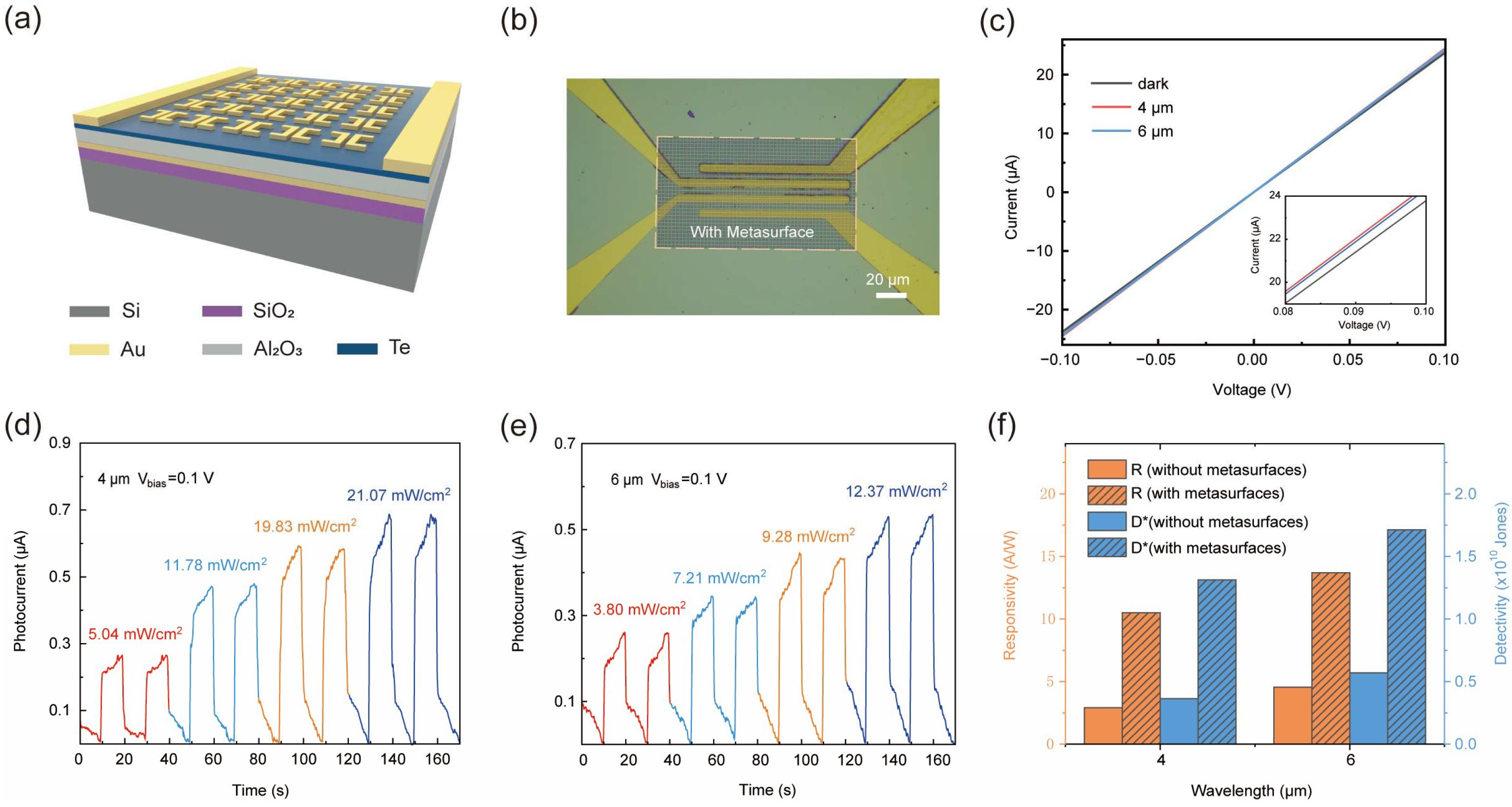
Figure 4a shows the metasurface-enhanced schematic diagram of a Te thin-film photodetector.
Figure 4b and
Figure S6 present the optical images of the device and the morphology of the metasurface structure. In the fabricated finger electrode device, the spacing between the electrodes is 5 μm and the electrode length is 100 μm. Approximately 84 double-C-shaped ring structures are arranged between the electrodes. As depicted in
Figure S7, we carried out FTIR tests on the Te thin-film devices featuring metasurface structures. In the wavelength range of 3–8 μm, two distinct absorption peaks were observed, situated at 4.2 μm and 6.2 μm, respectively, with absorption intensities of 0.58 and 0.51. Both peak positions experienced a red shift, and the absorption intensity decreased. This phenomenon may be attributed to the deviation between the optical structure and the design outcome during device processing.
Figure 4c shows the I–V characteristic measurement of the device, displaying a dark current of 23.9 μA at a bias of 0.1 V. In the enlarged view, the device exhibits clear photocurrent responses when excited by 4 μm and 6 μm lasers. The strictly linear behavior exhibited by both the dark-state and illuminated I–V curves provides definitive evidence of an ideal ohmic contact formed at the electrode–Te film interface. This linearity confirms that carrier transport across the interface is unimpeded by energy barriers, with current responding proportionally to applied bias under both dark and photoexcited conditions. The device’s photocurrent under 4 μm laser excitation is shown in
Figure 4d, increasing from 0.265 μA to 0.685 μA as the optical power density rises from 5.04 mW/cm
2 to 21.07 mW/cm
2.
Figure 4e presents the photocurrent response of the device under 6 μm laser excitation as a function of optical power density, yielding a net photocurrent of 0.534 μA at 12.37 mW/cm
2.
Figure S8 directly compares the performance of the initial Te thin-film device with the metasurface-enhanced counterpart, illustrating the impact of the designed metasurface structure. At 4 μm and 6 μm wavelengths, metasurfaces enhance the photocurrent of Te thin-film photodetectors by factors of 3.6 and 3.0, increasing from 0.191 μA and 0.177 μA to 0.685 μA and 0.534 μA, respectively. The designed metasurface structure in this work excites strong localized plasmonic resonances at 4 μm and 6 μm wavelengths, significantly enhancing the near-field intensity of incident light and increasing the light absorption of the Te thin film by eight times, thereby greatly improving the conversion efficiency of photons to electron–hole pairs. The band structure of Te is highly matched with mid-infrared photon energies, enabling the enhanced localized optical field to efficiently excite intrinsic carriers, while its high carrier mobility ensures rapid transport of photogenerated carriers. Band bending and a Schottky barrier formed at the interface between the metasurface and the Te film effectively separate photogenerated electrons and holes, suppress recombination losses, and enable directional injection of majority carriers into the electrodes. This mechanism allows the metasurface-enhanced Te thin-film device to achieve highly efficient mid-infrared photodetection. The dark current noise density of the Te thin-film photodetector is presented in
Figure S9. The current noise spectral density of the device is 1 × 10
−23 A
2/Hz at high frequencies, where white noise dominates, and increases to 1 × 10
−22 A
2/Hz at low frequencies, dominated by 1/f noise. As illustrated in
Figure 4f, the responsivity (R) and detectivity (D*) of Te thin-film photodetectors are markedly enhanced by the metal metasurface across the near-to-mid-infrared spectral range, as revealed by comparative measurements under varying laser excitation. Under 808 nm laser excitation, the R and D* of the Te thin-film photodetector are enhanced from 15.9 A/W and 1.99 × 10
10 Jones (without metasurface) to 60.5 A/W and 7.56 × 10
10 Jones (with metasurface), representing a 3.8-fold improvement attributable to the metasurface architecture. Under other near-infrared wavelengths, the R and D* of the device are improved by factors of 2.2 (1064 nm), 2.5 (1342 nm), and 2.1 (1550 nm), respectively. Under 4 μm excitation, the R and D* of the device reach 10.5 A/W and 1.31 × 10
10 Jones, representing a 3.6-fold enhancement relative to the pristine Te film. At 6 μm, these values increase to 13.7 A/W and 1.71 × 10
10 Jones, corresponding to a 3-fold improvement.