
Article

Photo–Hall Effect Characteristics of InAs/GaAs Quantum Dot Photoconductors with Sub-Bandgap Photoexcitation


1
Office for Academic and Industrial Innovations (Oacis), Kobe University, 1-1 Rokkodai, Nada, Kobe 657-8501, Hyogo, Japan
2
Department of Electrical Engineering and Computer Science, National Institute of Technology, Matsue College, 14-4 Nishi-Ikumacho, Matsue 690-8518, Shimane, Japan
3
College of Industrial Technology, Nihon University, 1-2-1 Izumi-cho, Narashino 275-8575, Chiba, Japan
4
Graduate School of Engineering, Kobe University, 1-1 Rokkodai, Nada, Kobe 657-8501, Hyogo, Japan
5
Quantum Future Creative Device Development Center, The University of Electro-Communications, 1-5-1 Chofugaoka, Chofu 181-8585, Tokyo, Japan
*
Author to whom correspondence should be addressed.
Photonics 2026, 13(1), 59; https://doi.org/10.3390/photonics13010059
Submission received: 20 November 2025 / Revised: 19 December 2025 / Accepted: 6 January 2026 / Published: 8 January 2026
(This article belongs to the Section Optoelectronics and Optical Materials)

Abstract

The photoconductive properties of an InAs/GaAs quantum dot (QD) superlattice have been characterized using photo–Hall measurements under sub-bandgap illumination. The multi-stacked InAs/GaAs QD structure was grown using molecular beam epitaxy and photo–Hall effect measurements were performed under illumination using light-emitting diodes with three different emission wavelengths: 940 nm, 1300 nm, and 1550 nm. The results have shown that the sign reversal occurs in the Hall coefficient (RH) as the illumination wavelength changes: RH is negative at 940 nm and 1300 nm, and positive at 1550 nm. The photocurrent at 940 nm illumination is ascribed to the electron hole pair generation in QDs, whereas the photocurrent at 1550 nm is dominated by the hole current generated through the midgap states in the structure. A simplified rate equation model involving two-step photoexcitation through the midgap states has revealed that the dominant photocarriers and the Hall coefficient can change depending on the photoexcitation power. The steady-state photocurrent behavior including the observed sign reversal in the Hall coefficient has been interpreted by the proposed model.

1. Introduction

Currently, III-V compound semiconductor quantum dots (QDs) such as InAs/GaAs QDs are widely used in a variety of optoelectronic devices including lasers [1], light-emitting diodes [2], infrared intersub-band transition detectors [3], semiconductor optical amplifiers (SOAs) [4], intermediate band solar cells [5], and quantum information devices [6]. Although most of those devices are constructed with vertical heterojunction structures containing QD layers, lateral QD structures are used for photoconductive sensors and photoconductive antenna (PCA) devices for Terahertz (THz) wave generation and detection [7,8,9]. Recently, InAs/GaAs QD structures have been used for PCAs to respond to the growing needs of PCAs that can operate under 1550 nm wavelength photoexcitation using low-cost telecom lasers [10,11]. Those GaAs-based QDs are suitable for THz PCA applications because they exhibit very fast photocurrent relaxation under ultrafast pulse excitation due to the photocarrier lifetime shortening of QDs [9] as well as low dark current due to the large-bandgap GaAs used as the current transport material [12]. We have reported basic THz wave generation using undoped InAs/GaAs QD [11] and Er-doped InAs/InGaAs QD [10] structures under 1550 nm wavelength photoexcitation.
In designing and preparing lateral photoconductive materials for operation at the wavelength in the sub-bandgap region, not only should the properties of QD structures but also the properties of midgap states incorporated in the materials be properly known. The characterization of photoconductive materials is often performed by using photocurrent spectroscopy [13] and photovoltage measurement [14] and detailed properties of the deep levels are studied using thermally stimulated current (TSC) spectroscopy [15], deep-level transient spectroscopy (DLTS) [16], and photocurrent transient measurement [17]. Another technique useful for investigating those materials is photo–Hall effect measurement, which has been extensively used in recent studies on various semiconductors [18,19,20,21]. In our recent report, the basic photoconductive properties of InAs/GaAs QD superlattice structures have been studied using photo–Hall effect measurements [11]. It has been found that the Hall coefficient (RH) is negative at the photoexcitation wavelengths 940 nm and 1300 nm, but RH becomes positive when the wavelength increases to 1550 nm. Similar Hall coefficient sign reversal has been found in recent studies on other semiconductor materials such as CdMnTe [19] and CdZnTe [20] bulk crystals, both of which involve multiple deep levels, but there has been no detailed investigation on GaAs-based-QD-containing materials. The Hall coefficient sign reversal observed in our QD material indicated a change in the dominant carriers from electrons to holes with the increase in the photoexcitation wavelength, but details of the photoconduction mechanism have not been fully understood.
The main purpose of the present paper is to explore the basic mechanism of the wavelength-dependent photo–Hall effect in the InAs/GaAs QD material and elucidate the roles of the QDs and midgap states. In the following sections, we analyze the photo–Hall effect results in more detail by determining the densities of the photo-generated electrons and holes separately and by interpreting the Hall coefficient behavior on a basis of those data and a simplified rate equation model. The Hall coefficient sign reversal is reasonably understood in our model and the effects of QDs and midgap states are clarified.

2. Materials and Methods

The material structure was originally designed for enabling short carrier lifetimes by rapid capture into the QDs with the aim of being applied to photoconductive antenna devices for THz generation and detection. The QD composition and size should be adjusted for forming sufficiently deep states while maintaining the high material quality of both QDs and surrounding GaAs layers and not compromising the carrier transport properties in the GaAs-based transport layer. The QD sub-band wavelength of ~1200 nm has been selected in our case, for which the growth conditions have been well established. The materials used in our study are the same as those used in our earlier paper, and the details of the experimental procedures have been written there [11]. The essence of the materials and experimental methods is outlined in this section. A structure containing multi-stacked InAs/GaAs QD layers was grown on a semi-insulating (SI) GaAs (001) substrate using molecular beam epitaxy (MBE). A 150 nm-thick undoped GaAs buffer layer was deposited onto the substrate at 550 °C. A set of 20-period stacked QD/spacer pairs, consisting of self-assembled InAs QDs with a nominal thickness of 2.0 monolayers (ML) and a 50 nm-thick undoped GaAs spacer layer, was grown at 480 °C. The in-plane density of the QDs is approximately 1 × 1010 cm−2 [12]. Finally, a 30 nm-thick undoped GaAs layer was grown at a low temperature: 250 °C. The total thickness of the GaAs layers, which form the photocurrent transport layer, is 1180 nm. The grown wafer was subject to rapid thermal annealing at 400 °C for 10 min. Using this QD structure wafer, Hall bars with 400 μm length (in parallel with the [110] orientation) and 100 μm width were fabricated by mesa etching followed by Ti/Au electrode formation. QDs are made of InAs and their individual size is typically 20–30 nm in lateral base diameter and ~4 nm in height [22]. The vertical wave function coupling among stacked QD layers is negligible due to the thick GaAs spacer layers used in our structure, and the carrier transport properties in the GaAs-based photocurrent transport layer is considered not to be altered severely by the inclusion of QDs. In the present material structure, QDs are made of InAs and their individual size is typically 20–30 nm in lateral base diameter and 4 nm in height [22]. The vertical wave function coupling among stacked QD layers is negligible due to the thick GaAs spacer layers used in our structure, and the carrier transport properties in the GaAs-based photocurrent transport layer is considered not to be altered severely by the inclusion of QDs. The basic property of the fabricated Hall bar was evaluated using the standard Hall effect measurement. The dark sheet Hall coefficient was +8.05 × 1010 cm2/C indicating p-type conduction, the dark sheet resistivity was 167 MΩ/sq., the effective sheet carrier density was 7.75 × 10⁷/cm2, and the effective Hall mobility was 482 cm2/(Vs).
Photo–Hall measurements were performed under continuous wave infrared illumination at fixed power levels using light-emitting diodes (LEDs) with wavelengths of 940 nm (LED output power: 12 mW), 1300 nm (3.5 mW), and 1550 nm (4.0 mW). The LED was placed at the distance of approximately 3 mm apart from the Hall bar. For the photo–Hall measurements, a magnetic flux density of 3729 G was applied to the Hall bar in the Voigt configuration. For obtaining the Hall coefficient with precision, we applied the ac measurement scheme together with the double lock-in scheme [11,23], in which the electric field and magnetic field are modulated at different frequencies and the Hall voltage is evaluated from their product appearing at their difference frequency [11]. All the measurements were made at room temperature.

3. Results and Discussion

3.1. Photosensitivity Characteristics

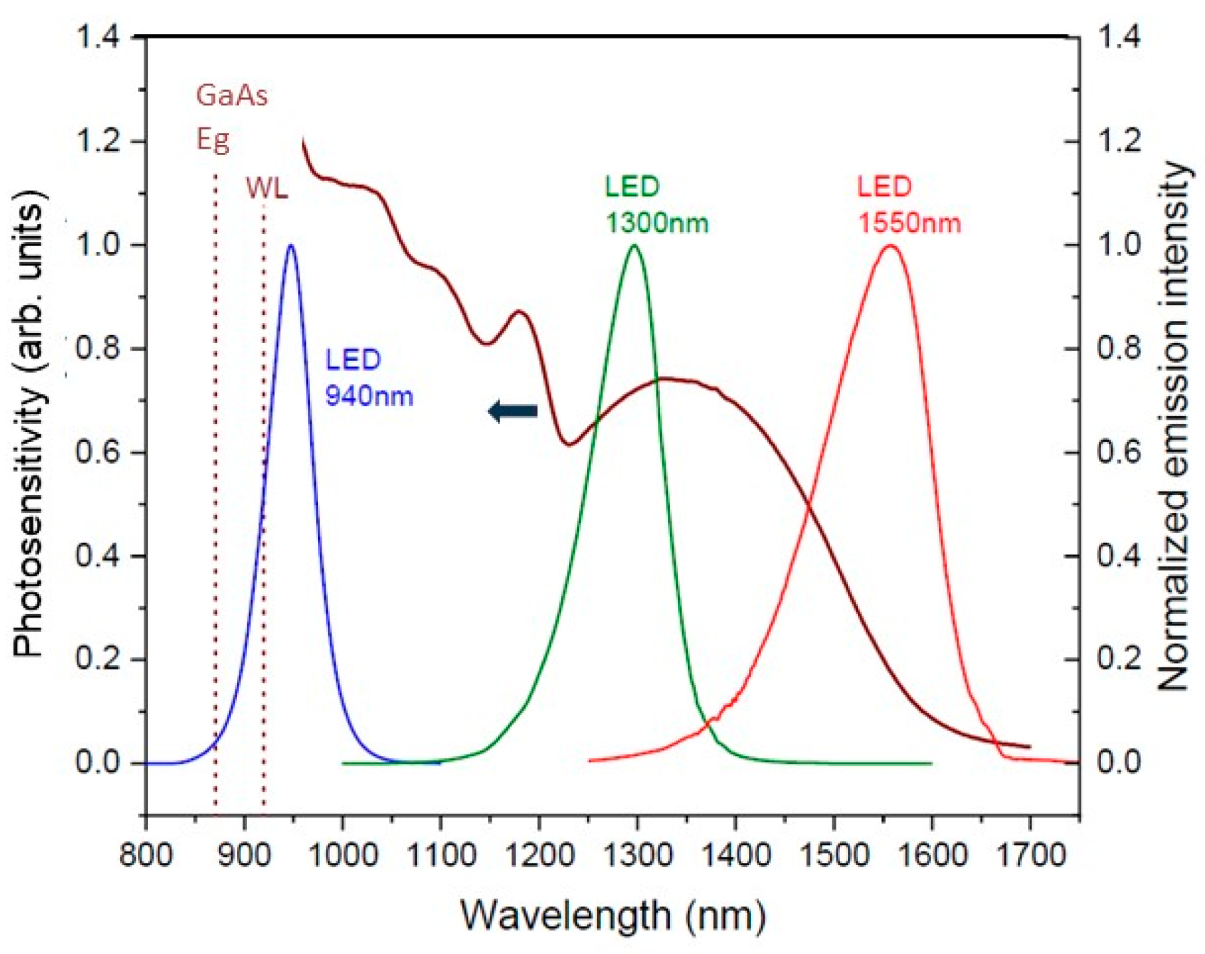
The photosensitivity spectra measured on the QD structure are shown in Figure 1, and the normalized emission spectra of the three LEDs used in the photo–Hall measurements are included for reference. The measured photosensitivity spectrum indicates several peaks including a couple of shoulders at 1031 nm, 1101 nm, and 1182 nm, and a broadened peak around 1345 nm. The observed photocurrent shoulders are attributed to the excited and ground state transitions in the QD with the 1182 nm (1.05 eV) wavelength corresponding to the ground state transition. The broad peak extending over ~1250–1600 nm (0.78–0.99 eV) would be ascribed to midgap states involved either in the GaAs transport layer or at the interface of or inside the QDs. The broadening might have been induced by the strain at the dot–spacer layer interface and/or enhanced by the interaction with interfacial states. Thus in the present material the 940 nm LED can excite QDs directly, and the 1550 nm LED can excite midgap states only. In the case of 1300 nm excitation, both the QDs and midgap states can be partially excited.

3.2. Photo–Hall Effect Measurements

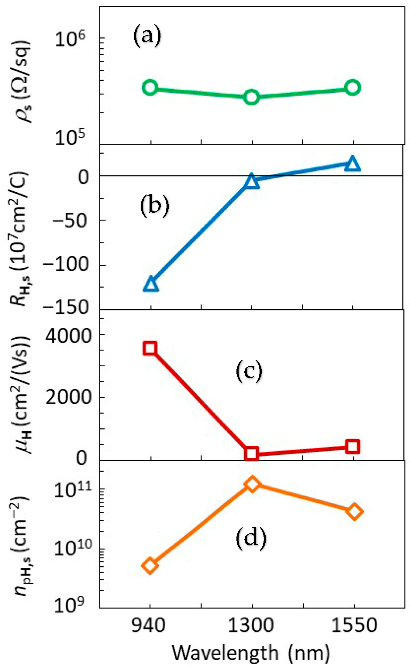
Figure 2 summarizes the result of the photo–Hall measurements including the sheet resistivity ρs, sheet Hall coefficient RH,s, Hall mobility μH = |RH,s|/ρs, and effective sheet carrier density npH,s = 1/(e|RH,s|), where e is the elementary charge [11]. The light intensity has been set at a level to give an approximately identical photoresistivity value for all wavelengths, as seen in Figure 2a. The Hall coefficient sign reversal occurs when the wavelength increases to 1550 nm. A negative Hall coefficient at shorter wavelengths indicates the dominant photo-generated carriers to be electrons, and this is consistent with the very large Hall mobility observed under 940 nm illumination. The Hall coefficient sign reversal at 1550 nm excitation indicates the dominance of the hole current.
To analyze details of the photocurrent transport, the densities of photo-generated electrons and holes need to be separately known. The resistivity (per unit volume) ρv = ρst, where t is the total thickness of GaAs transport layer (1180 nm), Hall coefficient RH,v = RH,st, electron and hole mobility μe and μh, and electron and hole densities n and p are correlated by the following basic equations:
ρ v = e p μ h + n μ e − 1 ,
R H , v = p μ h 2 − n μ e 2 e p μ h + n μ e 2 .
When the values of μe and μh are known, n and p can be determined from the following relations [17]:
n = μ h − R H , v / ρ v e ρ v μ e μ h + μ e ,
p = μ e + R H , v / ρ v e ρ v μ h μ h + μ e ,
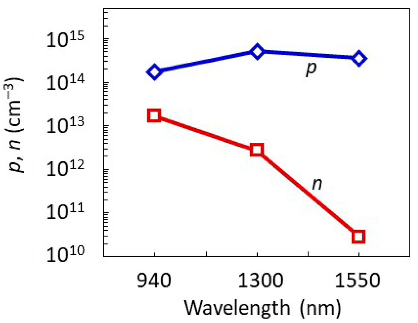
The defect density involved in MBE-grown GaAs materials varies in a wide range from <1015 cm−3 [24,25] to >1017 cm−3 [26,27] depending on the growth conditions. By taking into consideration our GaAs transport layer structure being composed of a combination of low-temperature-grown (LT-) GaAs, QD containing a spacer layer, and an undoped buffer layer, we assume 2 × 1016 cm−3 as an intermediate value in the following discussion. The mobility values for electrons and holes can be estimated by using the empirical relationship between the mobility and doping density as summarized by Sotoodeh [28] for a variety of growth methods and dopants. The mobility values expected at the doping density of 2 × 1016 cm−3 are ~5900 cm2/(Vs) for electrons and ~340 cm2/(Vs) for holes. The electron and hole densities evaluated from Equations (3) and (4) using those mobility values are shown in Figure 3, and all the parameters determined in the photo–Hall measurements are summarized in Table 1. It is noted that the hole mobility of 440 cm2/(Vs) has been used for the case of 1550 nm excitation to avoid an unreasonable (negative) value for n.
As has been described above, the considerably high density of electrons, comparable to that of holes, achieved at 940 nm photoexcitation results in a large negative Hall coefficient owing to the very high electron mobility, whereas the extremely low density of electrons at 1550 nm photoexcitation makes holes the dominant carriers and results in a Hall coefficient sign reversal. Under 940 nm photoexcitation, photocarriers are generated by the direct excitation of QDs. Under 1550 nm photoexcitation, the roles of QDs and midgap states in the carrier generation and transport are not clearly seen and further analyses are described below.

3.3. Band Structure Model and Rate Equation Analysis

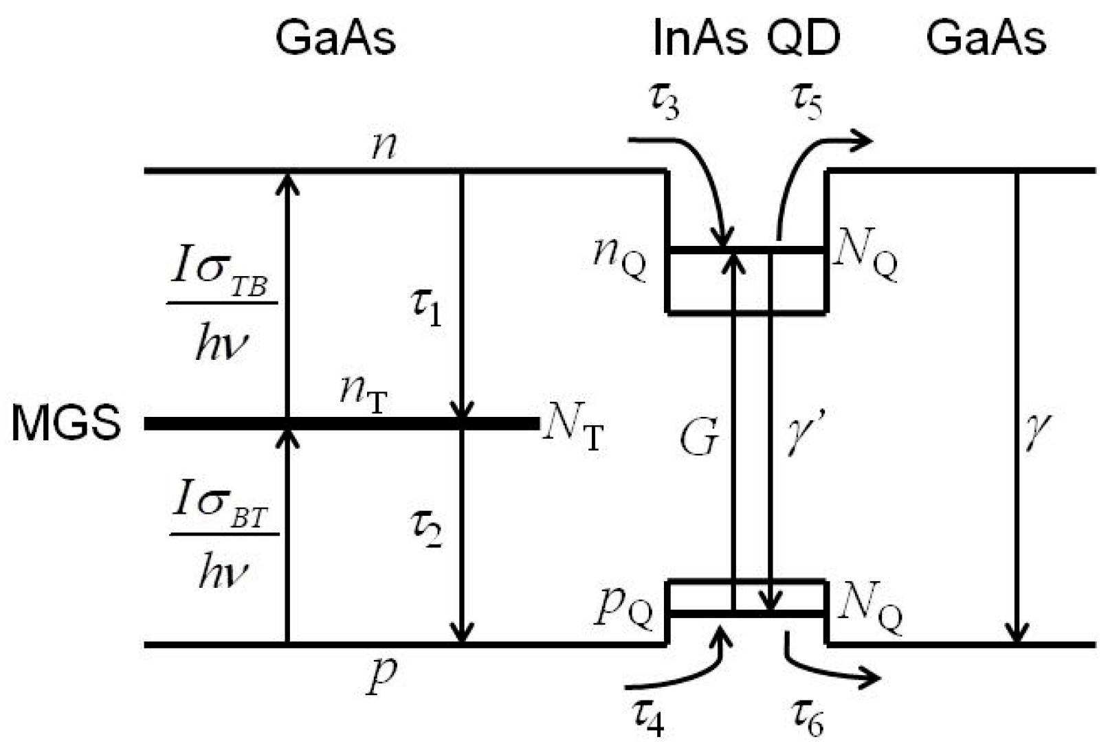
In this subsection, we discuss the photocarrier generation and transport by using a simplified band structure model and rate equation analysis with a particular focus on the photoexcitation at 940 nm and 1550 nm. Figure 4 shows a band structure model of the InAs/GaAs QD structure containing midgap states (MGSs). Under the photoexcitation of QDs, electron hole pairs are generated with the generation rate G in QDs and they contribute to the photocurrent flowing through the wetting layer and GaAs transport layer with the electron and hole densities n and p. The total state densities in the QD are defined as NQ in both conduction and valence bands, and the net electron and hole densities existing within the QDs are defined as nQ and pQ. τ3 and τ5 indicate time constants for electron capture from the conduction band into the QD state and for electron emission from the QD state to conduction band, respectively. Similarly, the hole capture and emission time constants from and to the valence band are defined as τ4 and τ6, respectively. For the photoexcitation at the wavelength much longer than the QD transition wavelength, we assume the two-step optical transition through the midgap states [29,30,31,32]. In this condition, the electron and hole generation rates are expressed by IσTB/hν and IσBT/hν, where σTB and σBT are the electron and hole photoexcitation cross sections, respectively, I is the photoexcitation power density, h is the Planck constant, and ν is the optical frequency. τ1 and τ2 are time constants for electrons to be trapped from the conduction band to the midgap state and the time constant for holes to be trapped from the valence band to the midgap state, respectively. The total density of the midgap states is defined as NT, in which nT is occupied by electrons. γ and γ’ are the recombination rates in the GaAs transport layer and QDs, respectively. To simplify the model, instead of introducing upper states in the GaAs conduction band [29,30,31,32], the time constants and capture cross sections are defined as the ones which involve the possible effects of upper valley states in the GaAs conduction band as well as the effects of excited sub-band states in the QDs.
In the following analysis, we focus on the low-power excitation regime in which our photo–Hall measurement has been made. A rate equation analysis for the excitation wavelength shorter than the QD sub-band wavelength has been reported by Golovynskyi [13]. Under low excitation conditions, it has been shown that ρv and RH,v show linear dependences on the generation rate G. Then it has also been shown that the electron and hole densities in the transport layer are expressed by n = τ3G and p = τ4G [13]. This result is useful for estimating the electron and hole capture time constants in QDs. Using the values of n and p evaluated under 940 nm photoexcitation as shown in Table 1, the ratio of τ4/τ3 is determined to be 10.4 independent of the photoexcitation intensity.
Under 1550 nm photoexcitation, the photocarrier generation is caused primarily by the midgap states. The basic rate equations for the overall photocurrent can be expressed, in the GaAs transport layer, by
d n d t = I σ T B h ν n T − n τ 1 − n τ 3 1 − n Q N Q + n Q τ 5 ,
d p d t = I σ B T h ν N T − n T − p τ 2 − p τ 4 1 − p Q N Q + p Q τ 6 ,
and in QDs, by
d n Q d t = n τ 3 − n Q τ 5 ,
d p Q d t = p τ 4 − p Q τ 6 .
In the present model for low photoexcitation intensity, the carrier recombination in both the transport layer and QDs are neglected. The charge neutrality condition in the transport layer is written by assuming midgap states with a hole trap nature as follows [33]:
n + n T + n Q = p + p Q .
For steady-state conditions, by equating the time derivatives of Equations (5)–(9) to be zero, we have the following relations:
n = I σ T B h ν τ 1 n T ,
p = I σ B T h ν τ 2 N T − n T ,
n T = I σ B T h ν τ 2 1 + τ 6 τ 4 1 + I σ T B h ν τ 1 1 + τ 5 τ 3 + I σ B T h ν τ 2 1 + τ 6 τ 4 N T ,
n Q = τ 5 τ 3 n ,
p Q = τ 6 τ 4 p
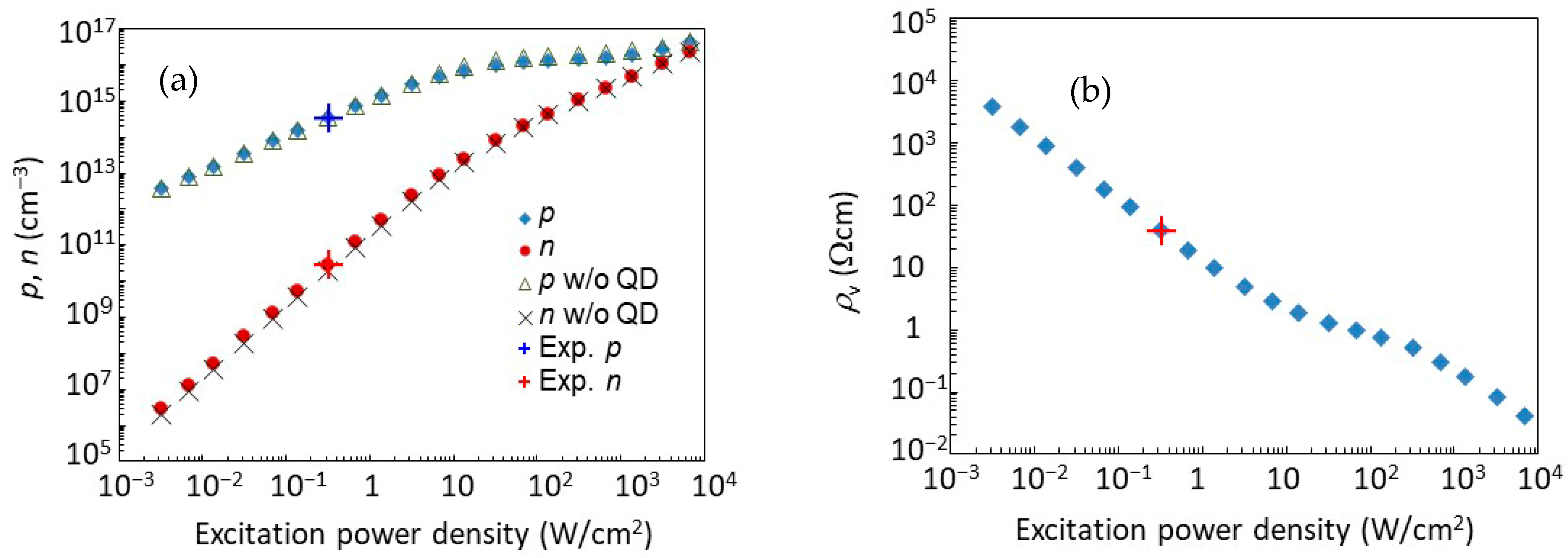
For understanding the behavior of these carrier densities, we have calculated the photoexcitation power density dependence of each density. The electron and hole capture cross sections of the midgap states are varied for fitting the calculated values of n and p with their corresponding experimental values, as shown in Table 1. The electron and hole time constants for capture by the midgap states are basically proportional to the reciprocal of their available destination state densities [34,35], and can be regarded as constant as long as the nT/NT value is not too close to unity or zero. In our steady-state calculation, we have assumed constant values as the long-term time constants for electrons and holes, τ1 = 7.1 ns and τ2 = 91 ns, to simplify the calculation. These values have been taken by referring to the range of recombination lifetimes for electrons and holes as reported on epitaxial GaAs layers [36,37,38]. Other parameter values necessary for the calculation have been taken from the literature: τ3 = 0.5 ps and τ4 = 5 ps [39] (being consistent with τ4/τ3 = ~10 as estimated from the 940 nm excitation case as described above), τ5 = 0.5 ps and τ6 = 2.5 ps [40,41]. The electron and hole state density NQ has been assumed to be 3.4 × 1016 cm−3 by taking account of not only the ground states but excited states in the QDs which have the actual QD density of 1.7 × 1015 cm−3 as determined from the atomic force microscope evaluation [12]. The obtained results of the dependences of various parameters as functions of the photoexcitation power density are displayed in Figure 5. In this calculation the capture cross section values have been assumed as σTB = 3.0 × 10⁻¹⁵ cm2 and σBT = 8.0 × 10⁻¹⁴ cm2. The hole capture cross section is larger than that for electrons as hole trap nature is considered. Similar cross section values have been reported on various deep levels including electron and hole traps in GaAs-based materials [16,42,43,44]. In Figure 5, the cross symbol in each figure indicates the experimental data obtained at the photoexcitation power density of 0.32 W/cm2.
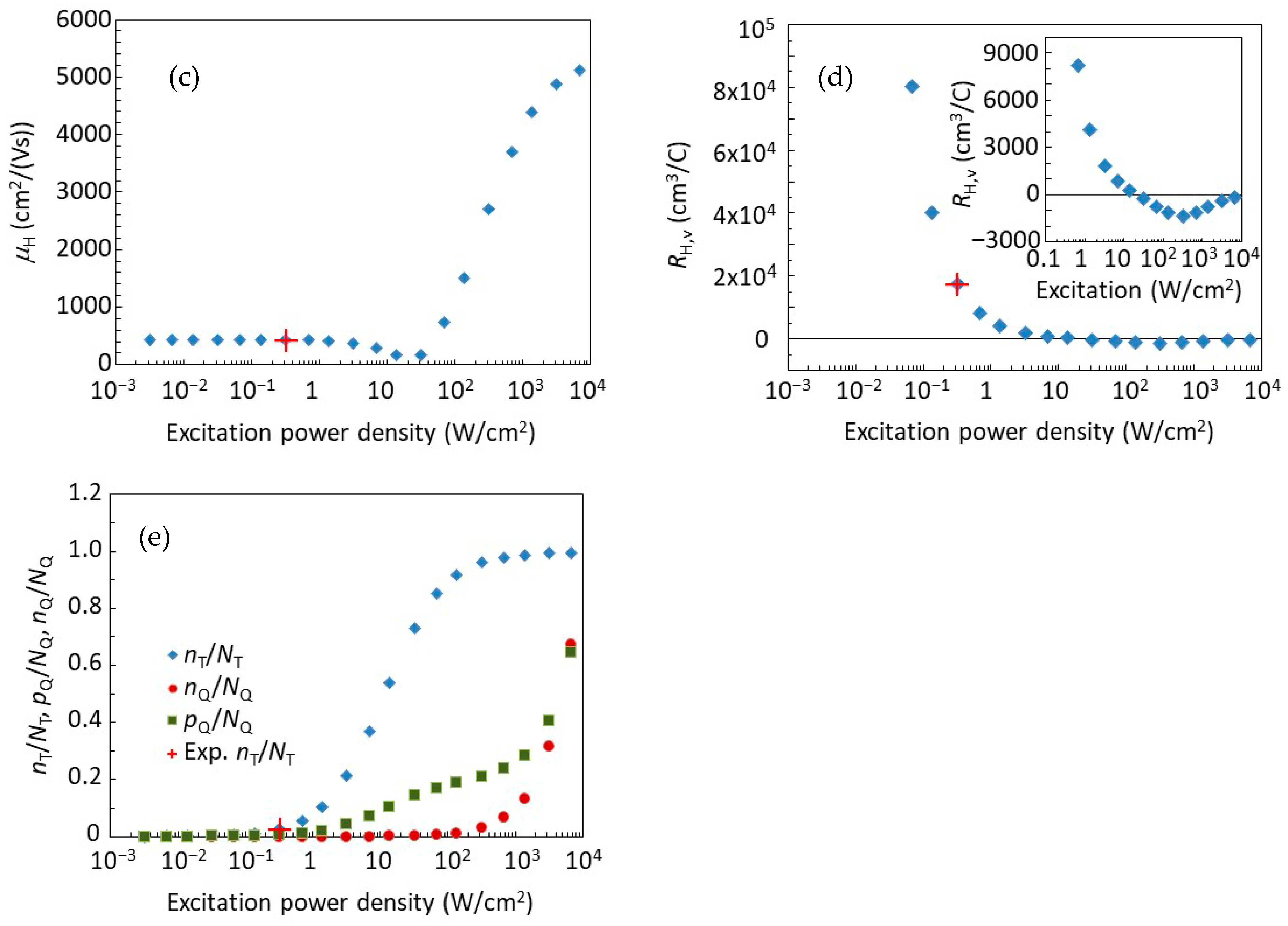
As shown in Figure 5a, the hole density increases linearly with the photoexcitation power density, whereas the electron density starts from a much smaller level but increases super-linearly with an exponent of ~3/2, and they look to eventually merge in a higher excitation region. The hole density saturation shown in the high excitation region is consistent with the midgap states becoming occupied as indicated by the increase in nT/NT in Figure 5e. In the transition region around the 10 W/cm2 excitation power density, an inflection occurs in the photoresistivity as well as in the Hall mobility and a sign change occurs in the Hall coefficient, as shown in Figure 5b–d. Thus, the Hall coefficient sign reversal found in our experiment is interpreted to be the interplay between the excitation intensity and carrier densities. Although the matching between the calculation and experiment has been performed only at a single excitation power density in this study, all the material parameters, as shown in Figure 5, have been consistently determined using the present model. This provides reasonable support to the viability of the proposed model and interpretation. In Figure 5a, the carrier densities calculated for the case without QDs are also plotted, but they show no significant difference from those with QDs. It is also seen in Figure 5e that carriers being trapped in QDs are negligibly small even in the high excitation region in our experiment. In the steady-state condition under the 1550 nm photoexcitation, the photocurrent generation and transport are governed by the midgap states. The situation may drastically change under the ultrafast laser pulse excitation usually adopted in PCA operation, where the lifetime-shortening effect caused by the QDs [9,12] plays a significant role in determining the photocurrent transient. More detail of this effect is subject to further research including the proper solution of the full rate equation and the precise measurement of the photocurrent transient.

4. Conclusions

An InAs/GaAs-QD-containing lateral photoconductor material has been analyzed using photo–Hall effect measurements under photoexcitation at different wavelengths. The Hall coefficient sign reversal has been found between 940 nm and 1550 nm. A simplified band structure and rate equation model, which involves two-step photoionization through the midgap state, have been used to discuss the mechanism of carrier generation and transport. Under QD excitation at 940 nm, the photo-generated carrier densities are linearly dependent on the excitation intensity, and the Hall coefficient is determined by the electrons. In contrast, under the midgap state excitation at 1550 nm, the photo-generated holes have orders of magnitude larger density than that for electrons, resulting in the Hall coefficient sign reversal. Although QDs show no explicit influence on the steady-state photocurrent, their effect on the photocarrier lifetime is suggested to impact the photocurrent transient and THz generation/detection properties. Through the present analysis, the roles of QDs and midgap states in photocurrent behavior have been substantially understood.

Author Contributions

Conceptualization, O.W.; methodology, O.W.; formal analysis, O.W.; investigation, O.W., Y.M., T.K. (Takahiro Kitada), and Y.H.; resources, Y.M., T.K. (Takahiro Kitada), T.K. (Toshiyuki Kaizu), and T.K. (Takashi Kita); writing—original draft preparation, O.W.; writing—review and editing, all authors; supervision, O.W.; funding acquisition, O.W., Y.M., and T.K. (Takahiro Kitada). All authors have read and agreed to the published version of the manuscript.

Funding

This work was funded in part by the Grants-in-Aid for Scientific Research (KAKENHI, Nos. 19K04532, 22K04218 and 23K25804) from the Japan Society for the Promotion of Science (JSPS).

Data Availability Statement

The raw data supporting the conclusions of this article will be made available by the authors on reasonable request.

Conflicts of Interest

The authors declare no conflicts of interest.

References

  1. Ledentsov, N.N.; Grundmann, M.; Heinrichsdorff, F.; Bimberg, D.; Ustinov, V.M.; Zhukov, A.E.; Maximov, M.V.; Alferov, Z.I.; Lott, J.A. Quantum-Dot Heterostructure Lasers. IEEE J. Sel. Top. Quantum Electron. 2000, 6, 439–451. [Google Scholar] [CrossRef] [Scilit]
  2. Ozaki, N.; Takeuchi, K.; Hino, Y.; Nakatani, Y.; Yasuda, T.; Ohkouchi, S.; Watanabe, E.; Ohsato, H.; Ikeda, N.; Sugimoto, Y.; et al. Integration of Emission-wavelength-controlled InAs Quantum Dots for Ultra broadband Near-infrared Light Source. Nanomater. Nanotechnol. 2014, 4, 26. [Google Scholar] [CrossRef] [Scilit]
  3. Kochman, B.; Stiff-Roberts, A.D.; Chakrabarti, S.; Phillips, J.D.; Krishna, S.; Singh, J.; Bhattacharya, P. Absorption, Carrier Lifetime, and Gain in InAs–GaAs Quantum-Dot Infrared Photodetectors. IEEE J. Quantum Electron. 2003, 39, 459–467. [Google Scholar] [CrossRef]
  4. Akiyama, T.; Sugawara, M.; Arakawa, Y. Quantum-dot semiconductor optical amplifiers. Proc. IEEE 2007, 95, 1757–1766. [Google Scholar] [CrossRef] [Scilit]
  5. Okada, Y.; Ekins-Daukes, N.J.; Kita, T.; Tamaki, R.; Yoshida, M.; Pusch, A.; Hess, O.; Phillips, C.C.; Farrell, D.J.; Yoshida, K.; et al. Intermediate band solar cells: Recent progress and future directions. Appl. Phys. Rev. 2015, 2, 021302. [Google Scholar] [CrossRef] [Scilit]
  6. Holmes, M.J.; Choi, K.; Kako, S.; Arita, M.; Arakawa, Y. Room-Temperature Triggered Single Photon Emission from a III Nitride Site-Controlled Nanowire Quantum Dot. Nano Lett. 2014, 14, 982–986. [Google Scholar] [CrossRef] [Scilit]
  7. Leyman, R.R.; Gorodetsky, A.; Bazieva, N.; Molis, G.; Krotkus, A.; Clarke, E.; Rafailov, E.U. Quantum dot materials for terahertz generation applications. Laser Photonics Rev. 2016, 10, 772–779. [Google Scholar] [CrossRef] [Scilit]
  8. Gorodetsky, A.; Lavrukhin, D.V.; Ponomarev, D.S.; Smirnov, S.V.; Yadav, A.; Khabibullin, R.A.; Rafailov, E.U. Enhanced THz generation from interdigitated quantum dot based photoconductive antenna operating in a quasi-ballistic regime. IEEE J. Select Top. Quantum Electron. 2023, 29, 8500505. [Google Scholar] [CrossRef] [Scilit]
  9. Gorodetsky, A.; Bazieva, N.; Rafailov, E.U. Pump dependent carrier lifetimes in InAs/GaAs quantum dot photoconductive terahertz antenna structures. J. Appl. Phys. 2019, 125, 151606. [Google Scholar] [CrossRef] [Scilit]
  10. Minami, Y.; Abe, H.; Lu, X.-M.; Kumagai, N.; Kitada, T. Terahertz wave emission with 1.5 μm pump from photoconductive antenna using stacked Er-doped-InAs quantum dot layers with ultrafast carrier relaxation. J. Appl. Phys. 2023, 134, 143101. [Google Scholar] [CrossRef] [Scilit]
  11. Minami, Y.; Simmen, A.; Kitada, T.; Harada, Y.; Kaizu, T.; Kojima, O.; Kita, T.; Wada, O. Photo-Hall effect characterization and terahertz wave generation with 1550 nm excitation in InAs/GaAs quantum dot superlattice based photoconductive antenna. J. Appl. Phys. 2025, 137, 213102. [Google Scholar] [CrossRef] [Scilit]
  12. Kaizu, T.; Kojima, O.; Minami, Y.; Kitada, T.; Harada, Y.; Kita, T.; Wada, O. Lateral photoconductivity of InAs/GaAs quantum dots for 1.5 μm-wavelength excitation photoconductive terahertz antenna devices. Jpn. J. Appl. Phys. 2024, 63, 082002. [Google Scholar] [CrossRef] [Scilit]
  13. Golovynskyi, S.L.; Dacenko, O.I.; Kondratenko, S.V.; Lavoryk, S.R.; Mazur, Y.I.; Wang, Z.M.; Ware, M.E.; Tarasov, G.G.; Salamo, G.J. Intensity-dependent nonlinearity of the lateral photoconductivity in InGaAs/GaAs dot-chain structures. J. Appl. Phys. 2016, 119, 184303. [Google Scholar] [CrossRef] [Scilit]
  14. Golovynskyi, S.; Seravalli, L.; Datsenko, O.; Kozak, O.; Kondratenko, S.V.; Trevisi, G.; Frigeri, P.; Gombia, E.; Lavoryk, S.R.; Golovynska, I.; et al. Bipolar effects in photovoltage of metamorphic InAs/InGaAs/GaAs quantum dot heterostructures: Characterization and design solutions for light-sensitive devices. Nanoscale Res. Lett. 2017, 12, 559. [Google Scholar] [CrossRef] [Scilit]
  15. Golovynskyi, S.; Datsenko, O.I.; Seravalli, L.; Trevisi, G.; Frigeri, P.; Babichuk, I.S.; Golovynska, I.; Li, B.; Qu, J. Defect influence on in-plane photocurrent of InAs/InGaAs quantum dot array: Long-term electron trapping and Coulomb screening. Nanotechnology 2019, 30, 305701. [Google Scholar] [CrossRef] [Scilit] [PubMed]
  16. Fregolent, M.; Buffolo, M.; De Santi, C.; Hasegawa, S.; Matsumura, J.; Nishinaka, H.; Yoshimoto, M.; Meneghesso, G.; Zanoni, E.; Meneghini, M. Deep levels and carrier capture kinetics in n-GaAsBi alloys investigated by deep level transient spectroscopy. J. Phys. D Appl. Phys. 2021, 54, 345109. [Google Scholar] [CrossRef] [Scilit]
  17. Kondratenko, S.V.; Iliash, S.A.; Vakulenko, O.V.; Mazur, Y.I.; Benamara, M.; Marega, E., Jr.; Salamo, G.J. Photoconductivity relaxation mechanisms of InGaAs/GaAs quantum dot chain structures. Nanoscale Res. Lett. 2017, 12, 183. [Google Scholar] [CrossRef] [Scilit]
  18. Bube, R.H. Photoelectronic Properties of Semiconductors; Cambridge University Press: Cambridge, UK, 1992; pp. 124–134. ISBN 9780521406819. [Google Scholar]
  19. Musiienko, A.; Grill, R.; Moravec, P.; Fochuk, P.; Vasylchenko, I.; Elhadidy, H.; Šedivý, L. Photo-Hall-Effect Spectroscopy with Enhanced Illumination in p-Cd1−xMnxTe Showing Negative Differential Photoconductivity. Phys. Rev. Appl. 2018, 10, 014019. [Google Scholar] [CrossRef] [Scilit]
  20. Musiienko, A.; Grill, R.; Hlídek, P.; Moravec, P.; Belas, E.; Zázvorka, J.; Korcsmáros, G.; Franc, J.; Vasylchenko, I. Deep levels in high resistive CdTe and CdZnTe explored by photo-Hall effect and photoluminescence spectroscopy. Semicond. Sci. Technol. 2017, 32, 015002. [Google Scholar] [CrossRef] [Scilit]
  21. Musiienko, A.; Yang, F.; Gries, T.W.; Frasca, C.; Friedrich, D.; Al-Ashouri, A.; Sağlamkaya, E.; Lang, F.; Kojda, D.; Huang, Y.-T.; et al. Resolving electron and hole transport properties in semiconductor materials by constant light-induced magneto transport. Nat. Commun. 2024, 15, 316. [Google Scholar] [CrossRef] [Scilit]
  22. Kaizu, T.; Tajiri, Y.; Kita, T. Wide-wavelength-range control of photoluminescence polarization in closely stacked InAs/GaAs quantum dots. J. Appl. Phys. 2019, 125, 234304. [Google Scholar] [CrossRef] [Scilit]
  23. Goree, J. Double lock-in detection for recovering weak coherent radio frequency signals. Rev. Sci. Instrum. 1985, 56, 1662–1664. [Google Scholar] [CrossRef] [Scilit]
  24. Lin, S.W.; Balocco, C.; Missous, M.; Peaker, A.R.; Song, A.M. Coexistence of deep levels with optically active InAs quantum dots. Phys. Rev. B 2005, 72, 165302. [Google Scholar] [CrossRef] [Scilit]
  25. Asano, T.; Fang, Z.; Madhukar, A. Deep levels in GaAs(001)/InAs/InGaAs/GaAs self-assembled quantum dot structures and their effect on quantum dot devices. J. Appl. Phys. 2010, 107, 073111. [Google Scholar] [CrossRef] [Scilit]
  26. Chan, M.H.; So, S.K.; Chan, K.T.; Kellert, F.G. Defect density measurements of low temperature grown molecular beam epitaxial GaAs by photothermal deflection spectroscopy. Appl. Phys. Lett. 1995, 67, 834–836. [Google Scholar] [CrossRef] [Scilit]
  27. Lin, G.R.; Liu, T.A.; Pan, C.L. Correlation between defect concentration and carrier lifetime of GaAs grown by molecular beam epitaxy at different temperatures. Jpn. J. Appl. Phys. 2001, 40, 6239–6242. [Google Scholar] [CrossRef] [Scilit]
  28. Sotoodeh, M.; Khalid, A.H.; Rezazadeh, A.A. Empirical low-field mobility model for III–V compounds applicable in device simulation. J. Appl. Phys. 2000, 87, 2890–2900. [Google Scholar] [CrossRef] [Scilit]
  29. Benjamin, S.D.; Loka, H.S.; Othonos, A.; Smith, P.W.E. Ultrafast dynamics of nonlinear absorption in low-temperature-grown GaAs. Appl. Phys. Lett. 1996, 68, 2544–2546. [Google Scholar] [CrossRef] [Scilit]
  30. Tani, M.; Lee, K.S.; Zhang, X.-C. Detection of terahertz radiation with low-temperature-grown GaAs-based photoconductive antenna using 1.55 µm probe. Appl. Phys. Lett. 2000, 77, 1396–1398. [Google Scholar] [CrossRef] [Scilit]
  31. Lee, C.K.; Yang, C.S.; Lin, S.H.; Huang, S.H.; Wada, O.; Pan, C.L. Effects of two-photon absorption on terahertz radiation generated by femtosecond-laser excited photoconductive antennas. Opt. Express 2011, 19, 23689–23697. [Google Scholar] [CrossRef] [Scilit] [PubMed]
  32. Jooshesh, A.; Fesharaki, F.; Bahrami-Yekta, V.; Mahtab, M.; Tiedje, T.; Darcie, T.E.; Gordon, R. Plasmon-enhanced LT-GaAs/AlAs heterostructure photoconductive antennas for sub-bandgap terahertz generation. Opt. Express 2017, 25, 22140–22148. [Google Scholar] [CrossRef] [Scilit]
  33. Würfel, P. Physics of Solar Cells: From Basic Principles to Advanced Concepts, 2nd ed.; Wiley-VCH: Weinheim, Germany, 2009; pp. 74–90. ISBN 978-3-527-40857-3. [Google Scholar]
  34. Gregory, I.S.; Tey, C.M.; Cullis, A.G.; Evans, M.J.; Beere, H.E.; Farrer, I. Two-trap model for carrier lifetime and resistivity behavior in partially annealed GaAs grown at low temperature. Phys. Rev. B 2006, 73, 195201. [Google Scholar] [CrossRef] [Scilit]
  35. Moazzami, K.; Murphy, T.E.; Phillips, J.D.; Cheung, M.C.-K.; Cartwright, A.N. Sub-bandgap photoconductivity in ZnO epilayers and extraction of trap density spectra. Semicond. Sci. Technol. 2006, 21, 717–723. [Google Scholar] [CrossRef] [Scilit]
  36. Niemeyer, M.; Kleinschmidt, P.; Lackner, D.; Walker, A.W.; Mundt, L.E.; Timm, C.; Lang, R.; Hannappel, T. Measurement of the non-radiative minority recombination lifetime and the effective radiative recombination coefficient in GaAs. AIP Adva. 2019, 9, 045034. [Google Scholar] [CrossRef] [Scilit]
  37. Andre, C.L.; Boeckl, J.J.; Wilt, D.M.; Pitera, A.J.; Lee, M.L.; Fitzgerald, E.A.; Keyes, B.M.; Ringel, S.A. Impact of dislocations on minority carrier electron and hole lifetimes in GaAs grown on metamorphic SiGe substrates. Appl. Phys. Lett. 2004, 84, 3447–3449. [Google Scholar] [CrossRef] [Scilit]
  38. Hooft, G.T.; van Opdorp, C.; Veenvliet, H.; Vink, A.T. Minority carrier lifetime and luminescence in MOVPE-grown (Al,Ga)As epilayers and DH lasers. J. Cryst. Growth 1981, 55, 173–182. [Google Scholar] [CrossRef] [Scilit]
  39. Yarotski, D.A.; Averitt, R.D.; Negre, N.; Crooker, S.A.; Taylor, A.J.; Donati, G.P.; Stintz, A.; Lester, L.F.; Malloy, K.J. Ultrafast carrier-relaxation dynamics in self-assembled InAs/GaAs quantum dots. J. Opt. Soc. Am. B 2002, 19, 1480–1484. [Google Scholar] [CrossRef] [Scilit]
  40. Geller, M.; Marent, A.; Stock, E.; Bimberg, D.; Zubkov, V.I.; Shulgunova, I.S.; Solomonov, A.V. Hole capture into self-organized InGaAs quantum dots. Appl. Phys. Lett. 2006, 89, 232105. [Google Scholar] [CrossRef] [Scilit]
  41. Kapteyn, C.M.A.; Lion, M.; Heitz, R.; Bimberg, D.; Brunkov, P.N.; Volovik, B.V.; Konnikov, S.G.; Kovsh, A.R.; Ustinov, V.M. Hole and electron emission from InAs quantum dots. Appl. Phys. Lett. 2000, 76, 1573–1575. [Google Scholar] [CrossRef] [Scilit]
  42. Ortiz, V.; Nagle, J.; Lampin, J.-F.; Péronne, E.; Alexandrou, A. Low-temperature-grown GaAs: Modeling of transient reflectivity experiments. J. Appl. Phys. 2007, 102, 043515. [Google Scholar] [CrossRef] [Scilit]
  43. Cavallini, A.; Fraboni, B.; Capotondi, F.; Sorba, L.; Biasiol, G. Deep levels in MBE grown AlGaAs/GaAs heterostructures. Microelectron. Eng. 2004, 73–74, 954–959. [Google Scholar] [CrossRef]
  44. Mitonneau, A.; Mircea, A.; Martin, G.M.; Pons, D. Electron and hole capture cross-sections at deep centers in gallium arsenide. Rev. Phys. Appl. 1979, 14, 853–861. [Google Scholar] [CrossRef] [Scilit]
Figure 1. Photosensitivity spectra measured on a Hall bar with the bias voltage of 3.6 V along the channel length of 400 μm. Normalized emission spectra of three LEDs used for the photo–Hall effect measurements are shown.
Photonics 13 00059 g001
Figure 2. (a) The sheet resistivity ρs, (b) sheet Hall coefficient RH,s, (c) Hall mobility μH, (d) sheet carrier density npH,s deduced from the photo–Hall measurement are shown for three different photoexcitation wavelengths.
Photonics 13 00059 g002
Figure 3. The electron and hole densities n and p determined from the photo–Hall effect measurements are shown for three different photoexcitation wavelengths.
Photonics 13 00059 g003
Figure 4. Band structure model used in the rate equation analysis.
Photonics 13 00059 g004
Figure 5. Calculated results of the photoexcitation power density dependence of (a) n and p, (b) ρv, (c) μH, (d) RH,v, (e) nT/NT, nQ/NQ, and pQ/NQ. The experimental plot of each parameter is indicated by a cross symbol.
Photonics 13 00059 g005aPhotonics 13 00059 g005b
Table 1. Summary of the photoexcitation wavelength, resistivity, and effective mobility determined from the photo–Hall measurements, and electron and hole mobility values used for carrier density determination as well as the resultant photo-generated hole and electron densities.
λ
(nm)
ρv
(Ωcm)
RH,v
(cm3/C)
μH
(cm2/(Vs))
μe
(cm2/(Vs))
μh
(cm2/(Vs))
n
(cm−3)
p
(cm−3)
94039.8−1.42 × 105355059003401.66 × 10131.73 × 1014
130032.3−6.03 × 10318759003402.76 × 10125.20 × 1014
155039.81.72 × 10443359004402.84 × 10103.56 × 1014
Disclaimer/Publisher’s Note: The statements, opinions and data contained in all publications are solely those of the individual author(s) and contributor(s) and not of MDPI and/or the editor(s). MDPI and/or the editor(s) disclaim responsibility for any injury to people or property resulting from any ideas, methods, instructions or products referred to in the content.