Communication

An Ultra-Compact InP 1310/1550 nm Wavelength Division (De)multiplexer Based on Channel-Shaped MMI Coupler

1
State Key Laboratory of Optoelectronic Materials and Devices, Institute of Semiconductors, Chinese Academy of Sciences, Beijing 100083, China
2
Center of Materials Science and Optoelectronics Engineering, University of Chinese Academy of Sciences, Beijing 100083, China
3
Beijing Key Laboratory of Low Dimensional Semiconductor Materials and Devices, Beijing 100083, China
*
Author to whom correspondence should be addressed.
Photonics 2025, 12(9), 922; https://doi.org/10.3390/photonics12090922
Submission received: 11 July 2025 / Revised: 10 September 2025 / Accepted: 15 September 2025 / Published: 16 September 2025
(This article belongs to the Section Optical Communication and Network)

Abstract

An ultra-compact 1310/1550 nm wavelength division (de)multiplexer based on a channel-shaped multimode interference structure was proposed and fabricated on an InP platform. The device has been simulated and optimized with a low insertion loss of 0.1 dB at 1310 nm wavelength and 0.33 dB at 1550 nm wavelength. The device features a notably compact footprint with an MMI region just 48 μm in length. Measurements revealed extinction ratios of 7.1 dB at 1310 nm and 5.9 dB at 1550 nm, accompanied by insertion losses of 7.07 dB and 3.03 dB for these wavelengths.

1. Introduction

Wavelength division multiplexing and demultiplexing (WDM) technology has become a cornerstone of contemporary optical communication infrastructure. As the demand for high-speed data transmission increases, particularly with the advent of 5G technology and the growing need for cloud computing and data center interconnects, WDM systems are essential for enhancing bandwidth and capacity [1,2]. The wavelengths of 1310 nm and 1550 nm are commonly employed in fiber-to-the-home (FTTH) networks, long distance transmissions, metro networks [3], passive optical networks, and multi-gas sensing areas [4]. It follows that 1310/1550 nm wavelength multiplexer and demultiplexers are indispensable components in such multiwavelength systems.
A variety of structures have been proposed for implementing WDM functions including directional couplers [5,6], arrayed waveguide gratings (AWGs) [7,8,9,10,11], etched-diffraction gratings (EDGs) [12], micro-ring resonators (MRRs) [13,14,15], asymmetric Mach–Zehnder interferometers (MZIs) [16], and multimode interference (MMI) couplers [17,18]. Among them, AWGs are susceptible to polarization and temperature variations, while EDGs require precise fabrication to ensure great grating facets. MRRs encounter difficulties in achieving uniform channel spacing as a result of fabrication deviation [7]. MMI structures stand out because of their high fabrication tolerance and low insertion loss [3,19,20]. However, when implementing a WDM function that supports both 1310 nm and 1550 nm wavelengths, the MMI typically exhibits a very large footprint [21].
Currently, MMI-based WDM structures have been realized on thin-film lithium niobate (TFLN) [22], silicon-on-insulator (SOI) [17,23] and indium phosphide (InP) platforms [3]. SOI platforms are favored for their high-contrast refractive index and compatibility with the complementary metal–oxide–semiconductor (CMOS) process [21,24]. However, the integration of silicon-based devices with III-V semiconductor lasers presents challenges in terms of complexity and cost. Compared to silicon platforms, InP platforms offer the advantage of monolithically integrating active and passive devices on a single wafer. However, conventional InP-based MMI structures are typically larger due to smaller refractive index differences. Developing new MMI structures on InP platforms to reduce the device size is of significant importance for the advancement of InP-based photonic integrated circuits.
In this paper, we demonstrate a novel compact channel-shaped MMI structure, which could enhance light confinement along the two sides of the multimode interference region. This design enables the effective combination and separation of different wavelengths, reducing the overall length of the WDM device. The performance of the proposed device is stimulated and demonstrated, showing an ultra-compact footprint with an MMI region just 48 μm in length.

2. Design and Simulation

For an MMI, the input mode pattern repeats itself at a distance of 3 L π , where L π is defined as the beat length:
L π   =   π β 0     β 1 4 n r W e 2 3 λ 0
where β 0 and β 1 denote the propagation constants of the fundamental and first-order modes, respectively. When two wavelengths (e.g., 1310 nm and 1550 nm) are introduced through a shared input port, the MMI region’s length needs to meet the following requirements to ensure their separation at different output ports:
L mmi   =   m 3 L π   1310   =   n ( 3 L π   1550 )
where m and n are integers of opposite parity (one even and one odd). This parity requirement is critical because it ensures that the two wavelengths form distinct images at the output port: the wavelength corresponding to the even integer forms a direct image, while the other forms a mirrored image. This is necessary to achieve the spatial separation of the two wavelengths at a specific position. To reduce the length of the device, a channel-shaped MMI structure was proposed in [25], which only supports the interference of the fundamental and first-order modes. Figure 1a,b show the sectional diagrams of the device and the cross-section of the channel-shaped waveguide. In our design, the channel thickness matches that of the core InGaAsP layer to relax fabrication tolerance, differing from the structure reported in [25].
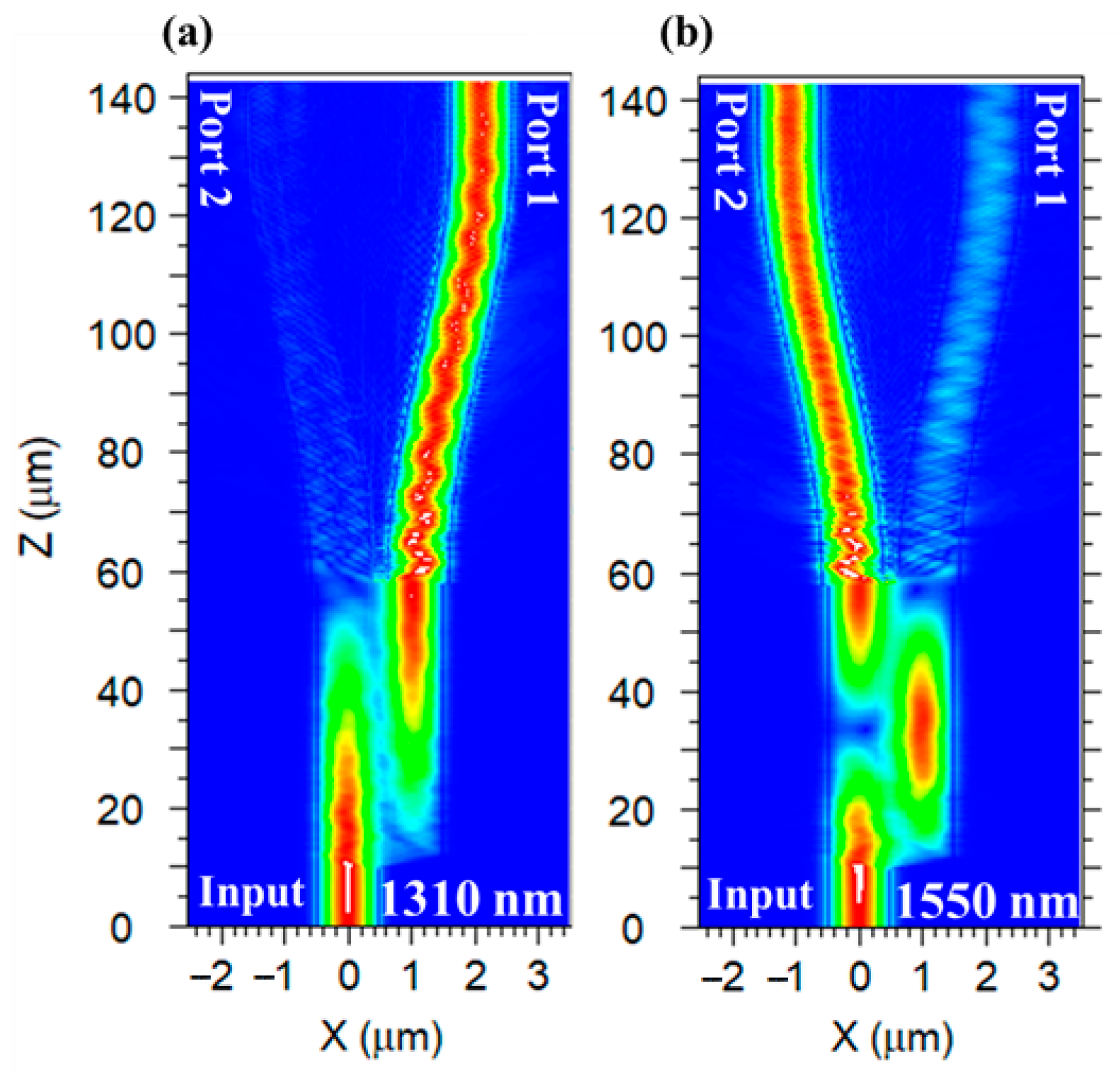
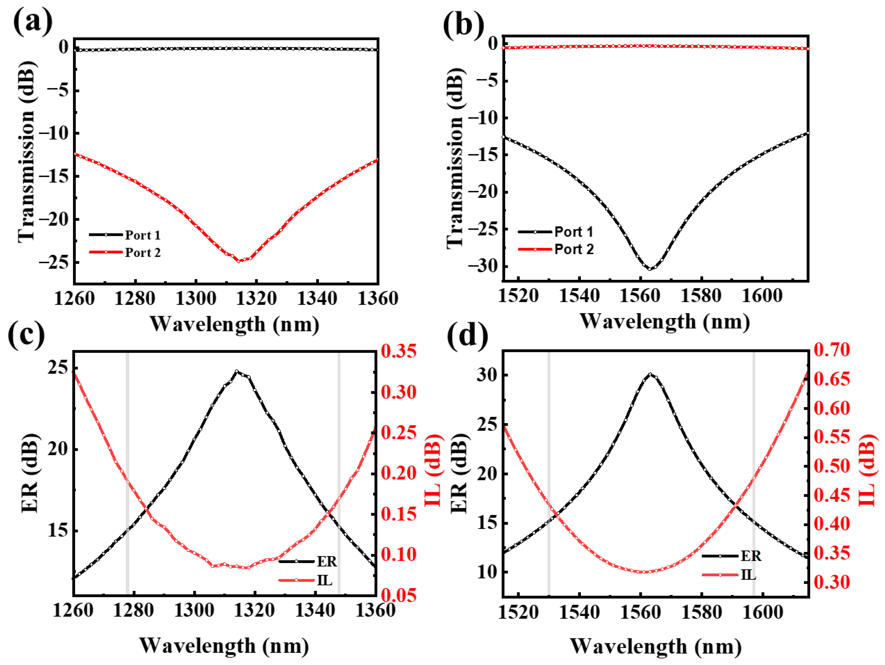
Figure 1a,b present the sectional diagrams of the device and the cross-section of the channel-shaped waveguide, respectively. In our design, the channel thickness matches that of the core InGaAsP layer to relax fabrication tolerance, differing from the structure reported in Ref. [22]. The presence of the channel provides two interference sections that confine the light in a narrow area along the direction of propagation, reducing the number of supported modes. The three-dimensional beam propagation method (3D-BPM) is used to simulate the effect of the performance of the device. We simulated different parameters, including the length of the MMI section, the width of MMI, and the channel width to achieve optimal performance. The fabrication tolerances of these parameters are illustrated in Figure 2a–f. A deviation of ±5 μm in the MMI length leads to a deterioration of the extinction ratio by over 10 dB. It can be concluded from Figure 2b,e that the MMI width tolerance needs to be kept within a range of ±100 nm to ensure a stable performance. Additionally, the channel width should be controlled within the range of 370–440 nm, as this interval is critical for achieving better device performance. Eventually, the device parameters are optimized with L m m i   =   48   μ m ,   W m m i   =   2   μ m ,   and   W s l o t   =   400   nm . Figure 3 demonstrates the successful propagation and separation of 1310 nm and 1550 nm wavelengths through the optimized structure, with each wavelength channeled to its designated output port (Port 1 and Port 2, respectively). The transmission spectra as a function of wavelength are shown in Figure 4a,b, with a designed center wavelength of 1310 nm and 1550 nm, respectively. Figure 4c,d illustrate the ER and IL performance at different wavelengths. It can be observed that with the wavelength range extending from 1278 nm to 1346 nm, the results show an extinction ratio (ER) exceeding 15 dB and insertion loss (IL) below 0.2 dB. Additionally, for the 1530–1597 nm range, the ER remains above 15 dB while the IL stays below 0.5 dB.

3. Fabrication and Measurement

The device is fabricated on the InP platform by using a two-step, low-pressure metal–organic chemical vapor deposition (MOCVD) process. In the first MOCVD process, a 600 nm InGaAsP core layer is deposited on the InP wafer. The photoluminescence wavelength of this layer is 1.2 μm. Then, a 400 nm channel is patterned on the InGaAsP layer using electron beam lithography, followed by inductively coupled plasma (ICP) dry etching. The second MOCVD process then deposits a 1 μm InP cladding layer over the entire structure. The deep ridge waveguide structure was completed using standard contact lithography and ICP etching processes. The scanning electron microscope (SEM) images of the cross-section and top view of the MMI section are shown in Figure 5. Figure 5a shows that the width of the waveguide is 2.039 μm, which is consistent with the design value. Figure 5b reveals that the effective length of the MMI section is actually extended by approximately 10 μm. This extension resulted from the merging of the two output channels, which began at the junction of the S-bend and the MMI section.
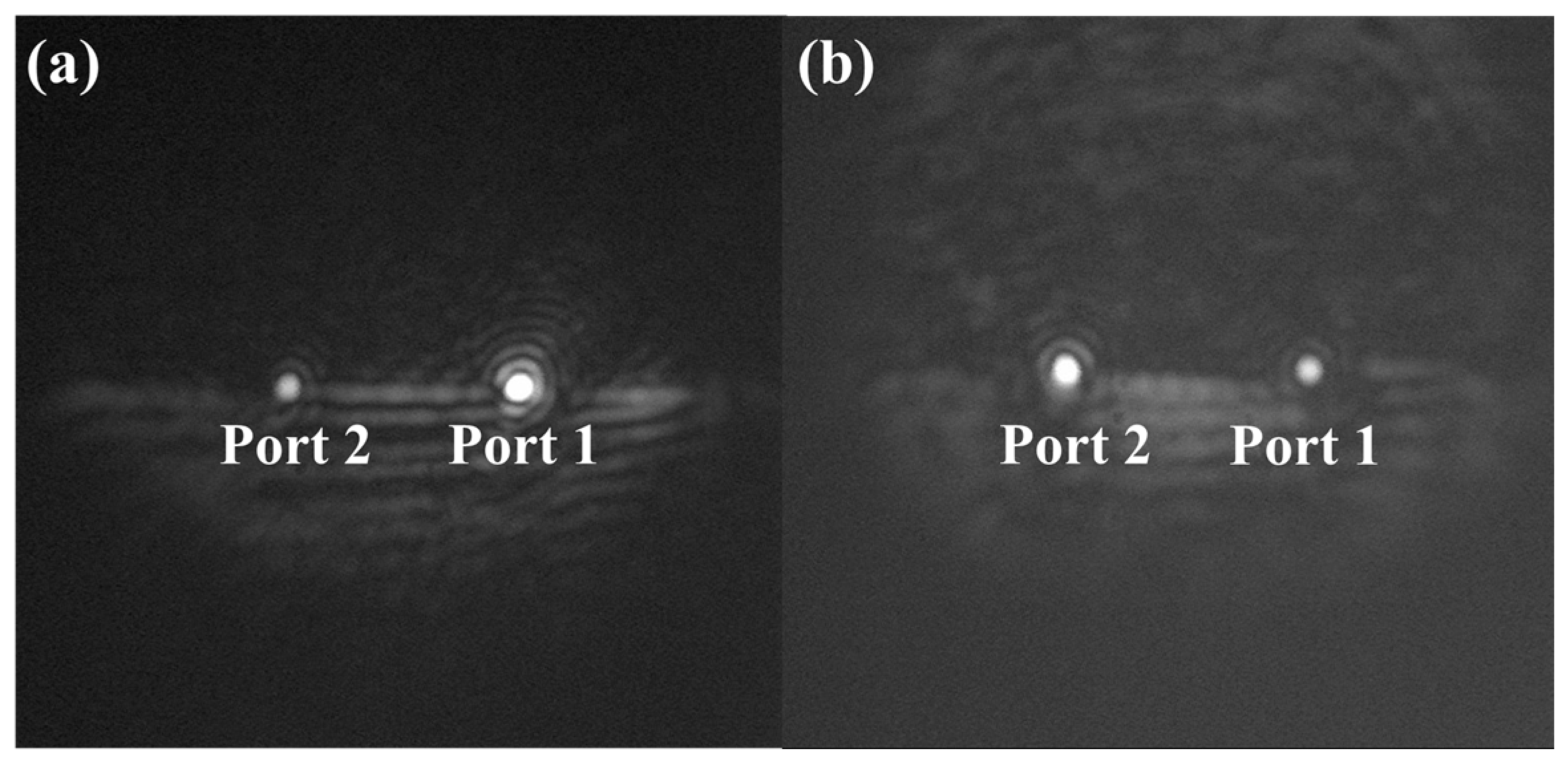
The performance of the device was characterized by using Original band (O-band) and Conventional band (C-band) light provided by two tunable single-mode lasers. Input light was coupled into the device through a tapered fiber, with the polarization adjusted using a polarization controller. Output light was collected by an objective lens and subsequently split by a beam splitter, with 98% directed to a Ge photodetector for detection and the remainder imaged by a charge-coupled device (CCD) camera. Figure 6a,b present the spatial distribution of the output with an input wavelength of 1310 nm and 1550 nm, respectively. The images demonstrate wavelength-dependent routing: 1310 nm light primarily exits through Port 1, while 1550 nm light predominantly emerges from Port 2. A minor portion of light appears at the opposite port due to manufacturing imperfections, which slightly degrades the device’s extinction ratio.
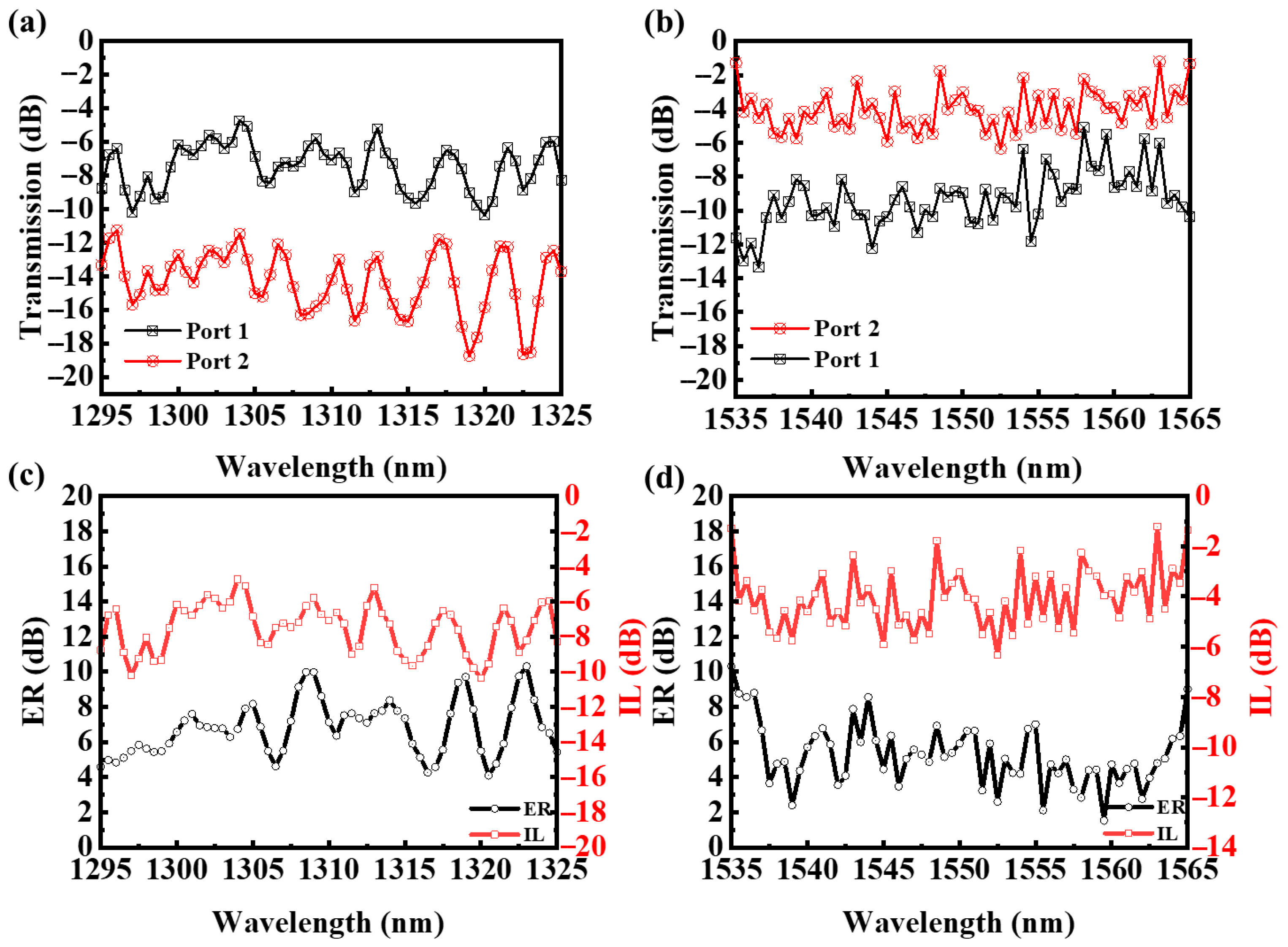
The ER and IL performances of the device were evaluated and shown in Figure 7a–d when illuminated using O-band and C-band lasers, respectively. The transmission curves of the device are wavelength-dependent oscillations, which are caused by the presence of the Fabry–Perot Cavity. All measurements were normalized to a reference straight waveguide of equal length. Experimental results demonstrate an ER of 7.1 dB and IL of 7.07 dB at 1310 nm, while at 1550 nm, the ER measured 5.9 dB with an IL of 3.03 dB. Notably, the device maintains an ER > 6.3 dB across 1307.5–1315 nm. Similarly, in the 1546.5–1551 nm range, the ER exceeds 4.8 dB relative to the 1550 nm reference. The device performance is not as good as predicted from the simulation, which may stem from fabrication imperfections. As illustrated in Figure 5b, the actual MMI length exhibits a significant deviation from the design value, attributable to unresolved branching connections at the MMI region due to lithography resolution limitations. This fabrication imperfection accounts for the discrepancy between the simulated and experimentally measured performance. Specifically, SEM measurements confirm that the fabricated MMI section reached approximately 58 μm—compared to the designed 48 μm—with the additional region corresponding to the unresolved branches. As shown in Figure 2, this length deviation can result in a ∼10 dB reduction in ER and a 1–2 dB increase in IL.
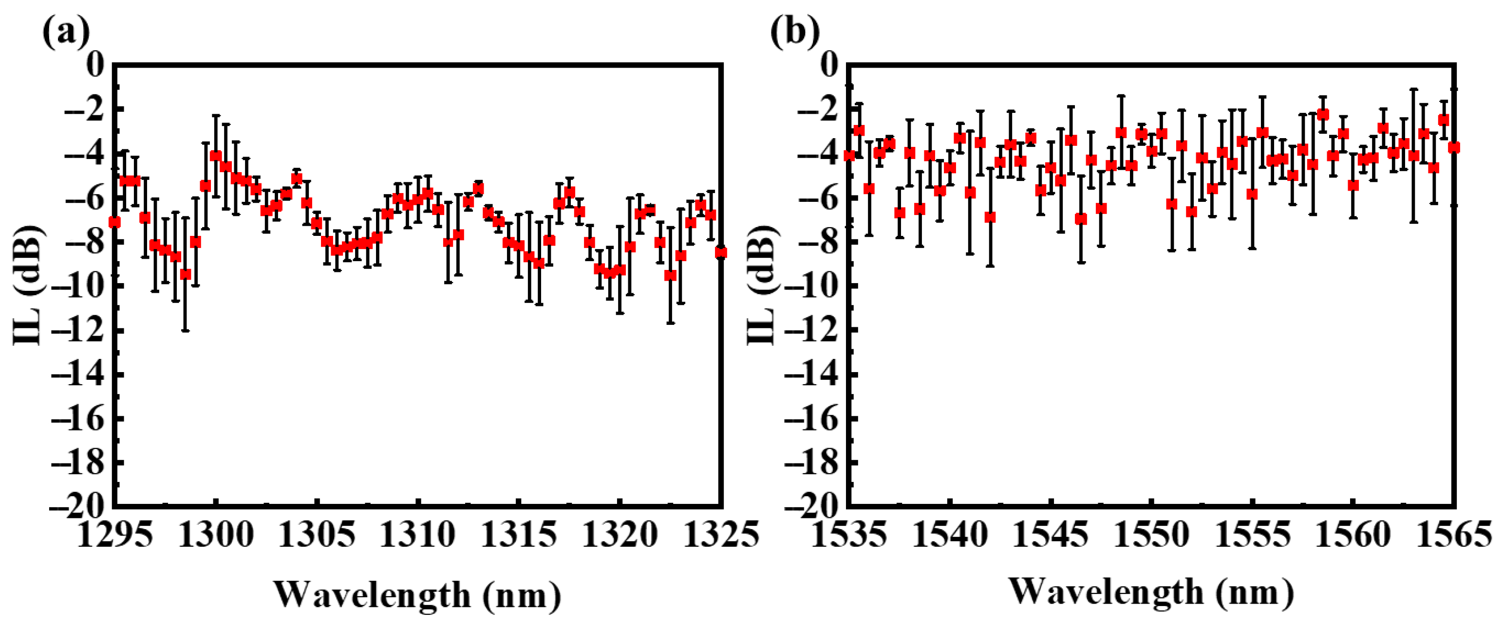
We also note that deviations in the ER from the designed value can affect IL measurements when evaluating loss in a two-port device. A lower ER results in greater excess loss, leading to a higher measured loss compared to single-port device measurements. The correlation between IL and ER, as shown in Figure 7c,d, demonstrates that when the ER deteriorates, the IL also increases. To further verify the impact of ER on IL, multiple devices were evaluated, as illustrated in Figure 8. The overall performance of the tested devices exhibits a similar correlation between IL and ER. Despite these fabrication imperfections, the device’s transmission characteristics remain qualitatively consistent with our wavelength division (de)multiplexer design. We anticipate an improved performance in both IL and ER once the fabrication precision issues are addressed.

4. Discussion

We compared the performance of this device with that of other MMI-based structures across different material platforms in Table 1. Compared with the traditional MMI structure reported in Ref. [3], the length of the MMI section in our design has been significantly reduced. Although the test results are inferior to the simulation results, we have verified the feasibility of this structure. In subsequent work, fabrication-induced deviation is expected to be mitigated by employing electron beam lithography (EBL), which offers significantly higher patterning precision and can better control the critical dimensions at the junction of the S-bend and MMI section, thereby avoiding the unintended extension of the MMI length.

5. Conclusions

In conclusion, we present a novel compact 1310/1550 nm wavelength division (de)multiplexer based on channel-shaped MMI structures. The proposed design features a significantly shorter MMI coupler length compared to conventional structures, while successfully achieving wavelength division multiplexing functionality. Experimental results confirm the structure’s feasibility, showing extinction ratios of 7.1 dB and 5.9 dB with insertion losses of 7.07 dB and 3.03 dB at 1310 nm and 1550 nm, respectively. In future work, we will optimize the simulation design, improve process precision, and further reduce the device size, which will facilitate the monolithic integration of the device with lasers. More importantly, this design can be extended to fabricate wavelength division multiplexers spanning the O-S-L bands, holding promising potential for applications in 50G PON systems.

Author Contributions

Conceptualization, F.G.; methodology, F.G.; software, F.G.; validation, F.G. and D.L.; formal analysis, W.Y.; investigation, W.Y.; resources, D.L.; data curation, W.Y. and M.Z.; writing—original draft preparation, W.Y.; writing—review and editing, D.L. and W.Y.; visualization, W.Y.; supervision, D.L. and F.G.; funding acquisition, D.L. All authors have read and agreed to the published version of the manuscript.

Funding

The work is supported by National Natural Science Foundation of China (61975197); the Self-Deployed Project of State Key Laboratory of Optoelectronic Materials and Devices (2023E375010001GF).

Institutional Review Board Statement

Not applicable.

Informed Consent Statement

Not applicable.

Data Availability Statement

Data is contained within the article.

Conflicts of Interest

The authors declare no conflicts of interest.

References

  1. Effenberger, F.J.; Zhang, D. WDM-PON for 5G Wireless Fronthaul. IEEE Wirel. Commun. 2022, 29, 94–99. [Google Scholar] [CrossRef]
  2. Skubic, B.; Bottari, G.; Öhlén, P.; Cavaliere, F. The Role of DWDM for 5G Transport. In Proceedings of the 2014 The European Conference on Optical Communication (ECOC), Cannes, France, 21–25 September 2014; pp. 1–3. [Google Scholar]
  3. Chack, D.; Kumar, V.; Raghuwanshi, S.K. Design and Performance Analysis of InP/InGaAsP-MMI Based 1310/1550 nm Wavelength Division Demultiplexer with Tapered Waveguide Geometry. Opto-Electron. Rev. 2015, 23, 271–277. [Google Scholar] [CrossRef]
  4. Thottoli, A.; Biagi, G.; Vorobev, A.S.; Giglio, M.; Magno, G.; O’Faolain, L.; Grande, M. Highly Efficient and Selective Integrated Directional Couplers for Multigas Sensing Applications. Sci. Rep. 2023, 13, 22720. [Google Scholar] [CrossRef]
  5. Chen, J. A Broadband Wavelength Demultiplexer Assisted by SWG-Based Directional Couplers. Optik 2020, 202, 163602. [Google Scholar] [CrossRef]
  6. Nikbakht, H.; Khoshmehr, M.T.; van Someren, B.; Teichrib, D.; Hammer, M.; Förstner, J.; Akca, B.I. Asymmetric, Non-Uniform 3-dB Directional Coupler with 300-Nm Bandwidth and a Small Footprint. Opt. Lett. 2023, 48, 207–210. [Google Scholar] [CrossRef]
  7. Chen, S.; Fu, X.; Wang, J.; Shi, Y.; He, S.; Dai, D. Compact Dense Wavelength-Division (De)Multiplexer Utilizing a Bidirectional Arrayed-Waveguide Grating Integrated with a Mach–Zehnder Interferometer. J. Light. Technol. 2015, 33, 2279–2285. [Google Scholar] [CrossRef]
  8. Wang, J.; Sheng, Z.; Li, L.; Pang, A.; Wu, A.; Li, W.; Wang, X.; Zou, S.; Qi, M.; Gan, F. Low-Loss and Low-Crosstalk 8 × 8 Silicon Nanowire AWG Routers Fabricated with CMOS Technology. Opt. Express 2014, 22, 9395–9403. [Google Scholar] [CrossRef]
  9. Zheng, Y.; Wu, X.; Jiang, L.; Wu, Y.; Duan, J. Design of 4-Channel AWG Multiplexer/Demultiplexer for CWDM System. Optik 2020, 201, 163513. [Google Scholar] [CrossRef]
  10. Li, S.; Zhang, J.; Wang, L.; You, J.; Wang, Y.; Yin, X.; Chen, J.; Sun, B.; An, J.; Wu, Y. The O-Band 20-Channel 800 GHz Arrayed Waveguide Grating Based on Silica Platform for 1 Tb/s or Higher-Speed Communication System. Opt. Laser Technol. 2022, 156, 108475. [Google Scholar] [CrossRef]
  11. Tu, H.; Zhang, Y.; Li, G.; Dai, X.; Wu, Y.; Zhang, Y.; Li, H.; Lu, Q.; Lu, M.; Guo, W. 100-Channel Arrayed Waveguide Grating Based on Thin Film Lithium Niobate on Insulator (LNOI). J. Light. Technol. 2024, 42, 4519–4524. [Google Scholar] [CrossRef]
  12. Song, J.; Zhu, N.; He, J.-J.; He, S. Etched Diffraction Grating Demultiplexers with Large Free-Spectral Range and Large Grating Facets. IEEE Photonics Technol. Lett. 2006, 18, 2695–2697. [Google Scholar] [CrossRef]
  13. Seifouri, M.; Fallahi, V.; Olyaee, S. Ultra-High-Q Optical Filter Based on Photonic Crystal Ring Resonator. Photon. Netw. Commun. 2018, 35, 225–230. [Google Scholar] [CrossRef]
  14. Neto, J.V.S.; Carvalho, W.O.F.; Mejía-Salazar, J.R. Magnetically Tunable Micro-Ring Resonators for Massive Magneto-Optical Modulation in Dense Wavelength Division Multiplexing Systems. Sensors 2022, 22, 8163. [Google Scholar] [CrossRef]
  15. Liu, D.; He, J.; Xiang, Y.; Xu, Y.; Dai, D. High-Performance Silicon Photonic Filters Based on All-Passive Tenth-Order Adiabatic Elliptical-Microrings. APL Photonics 2022, 7, 051303. [Google Scholar] [CrossRef]
  16. Cheung, S.S.; Tan, M.R.T. Silicon Nitride (Si3N4) (De-)Multiplexers for 1 mm CWDM Optical Interconnects. J. Light. Technol. 2020, 38, 3404–3413. [Google Scholar] [CrossRef]
  17. Zeng, G.; Yin, Y.; Ding, Y.; Yang, J.; Yan, J.; Sun, X.; Zhang, D. Temperature-Insensitive and Fabrication-Tolerant Coarse Wavelength Division (de)Multiplexing on a Silica Platform Using an Angled Multimode Interferometer. Opt. Express 2023, 31, 21161–21171. [Google Scholar] [CrossRef]
  18. Wang, F.; Xu, X.; Sun, C.; Zhao, J. Ultracompact 1310/1550 Nm Wavelength Demultiplexer Based on Subwavelength Grating-Assisted Multimode Interference Coupler. Opt. Eng. 2021, 60, 087104. [Google Scholar] [CrossRef]
  19. Khalilzadeh, H.; Bahrami, A.; Badri Ghavifekr, H. MMI-Based All-Optical Four-Channel Wavelength Division Demultiplexer. Photon. Netw. Commun. 2018, 36, 217–223. [Google Scholar] [CrossRef]
  20. Wei, S.; Jian, W.; Zhao, L.; Zhang, R.; Qiu, J.; Yin, Z.; Tian, Y. A Novel InP-Based 1.31/1.55 mm Wavelength Demultiplexer with Side-Port Multimode Interference Coupler. In Proceedings of the 2014 Conference on Lasers and Electro-Optics (CLEO)—Laser Science to Photonic Applications, San Jose, CA, USA, 8–13 June 2014; pp. 1–2. [Google Scholar]
  21. Zhang, J.; Xu, L.; Mao, D.; Xing, Z.; D’Mello, Y.; Jacques, M.; Wang, Y.; Lessard, S.; Plant, D.V. High-Extinction-Ratio and Compact 1310/1550 Nm Wavelength Diplexer on SOI Platform Based on an SWG-Structured Two-Mode Interference Coupler. IEEE Photonics J. 2022, 14, 1–6. [Google Scholar] [CrossRef]
  22. Chen, G.; Ruan, Z.; Wang, Z.; Huang, P.; Guo, C.; Dai, D.; Chen, K.; Liu, L. Four-Channel CWDM Device on a Thin-Film Lithium Niobate Platform Using an Angled Multimode Interferometer Structure. Photon. Res. 2021, 10, 01000008. [Google Scholar] [CrossRef]
  23. Shi, Y.; Chen, J.; Xu, H. Silicon-Based on-Chip Diplexing/Triplexing Technologies and Devices. Sci. China Inf. Sci. 2018, 61, 080402. [Google Scholar] [CrossRef]
  24. Chen, Y.; Wu, S.; Zhang, J.; Zhu, M.; Xiao, J. Compact Silicon-Based Polarization-Independent 1.55/2 mm Wavelength Diplexer Based on a Multimode Interference Coupler with Multiple Shallow Grooves. Opt. Laser Technol. 2022, 153, 108290. [Google Scholar] [CrossRef]
  25. Guo, F.; Lu, D.; Song, H.; Niu, Y.; Zhou, D.; Zhao, L. A Compact Triplexer Based on InP/InGaAsP-MMI Coupler with Channel-Shaped Core Layer for 50G PON. Photonics 2024, 11, 232. [Google Scholar] [CrossRef]
  26. Xu, L.; Wang, Y.; Mao, D.; El-Fiky, E.; Xing, Z.; Kumar, A.; Saber, M.G.; Jacques, M.; Plant, D.V. Broadband 1310/1550  nm Wavelength Demultiplexer Based on a Multimode Interference Coupler with Tapered Internal Photonic Crystal for the Silicon-on-Insulator Platform. Opt. Lett. 2019, 44, 1770–1773. [Google Scholar] [CrossRef] [PubMed]
  27. Wang, M.; Zhang, Z.; Xin, Y.; Fang, J.; Liu, T.; Sun, X.; Wu, Y.; Zhang, D. Compact Silica Dual-Band Wavelength Demultiplexer Based on Asymmetric-Defined Multimode Interference Coupler. Opt. Express 2025, 33, 3957–3969. [Google Scholar] [CrossRef]
Figure 1. (a) Section diagram of channel-shaped MMI device. (b) Cross-section of the channel-shaped waveguide.
Photonics 12 00922 g001
Figure 2. Fabrication tolerances at wavelengths of 1310 nm (ac) and 1550 nm (df), specifically regarding (a,d) the length of MMI, (b,e) the width of MMI, and (c,f) the width of the channel.
Photonics 12 00922 g002
Figure 3. Simulated propagations of wavelengths at (a) 1310 nm and (b) 1550 nm, where 1310 nm is the wavelength outputs from Port 1 and 1550 nm wavelength outputs from Port 2.
Photonics 12 00922 g003
Figure 4. Simulated transmission spectrum as a function of wavelength with a designed center wavelength of (a) 1310 nm and (b) 1550 nm and the corresponding (c,d) ER and IL performance, respectively.
Photonics 12 00922 g004
Figure 5. SEM images of the (a) cross-section image and (b) top view of the full device including input ports and output ports.
Photonics 12 00922 g005
Figure 6. The mode patterns obtained from Port 1 and Port 2 when illuminated at wavelengths of (a) 1310 nm and (b) 1550 nm.
Photonics 12 00922 g006
Figure 7. The transmission curves of Port 1 and Port 2 in the (a) O-band and (b) C-band, and the correspondingly calculated IL and ER performance of the device in the (c) O-band and (d) C-band.
Photonics 12 00922 g007
Figure 8. The error bar of IL as a function of wavelength in the (a) O-band and (b) C-band, calculated from three devices.
Photonics 12 00922 g008
Table 1. Comparative performance of MMI-based WDM device on diverse material platforms.
PlatformStructureIL (dB)
1310 nm/1550 nm
ER (dB)
1310 nm/1550 nm
Length (μm)MethodRef.
SOIMMI3.85/0.7232.6/16.4108.5Experiment[26]
SOIMMI0.315.2/16.834.5Simulation[18]
SilicaMMI1.43/0.8524.92/26.564000Experiment[27]
InPMMI0.25519.487240Simulation[3]
InPMMI/20/15298.5Experiment[20]
InPMMI0.1/0.3323.8/23.0248SimulationThis work
InPMMI7.07/3.037.1/5.948ExperimentThis work
Disclaimer/Publisher’s Note: The statements, opinions and data contained in all publications are solely those of the individual author(s) and contributor(s) and not of MDPI and/or the editor(s). MDPI and/or the editor(s) disclaim responsibility for any injury to people or property resulting from any ideas, methods, instructions or products referred to in the content.