Article

Measurement of Enhanced Inversion Factor of InGaAs-Based Well-Island Composite Structure by Photoluminescence Spectra from Dual Facets

1
School of Electronic Information Engineering, Wuxi University, Wuxi 214105, China
2
Jiangsu Province Engineering Research Center of Photonic Devices and System Integration for Communication Sensing Convergence, Wuxi University, Wuxi 214105, China
*
Author to whom correspondence should be addressed.
Photonics 2025, 12(9), 834; https://doi.org/10.3390/photonics12090834
Submission received: 23 July 2025 / Revised: 10 August 2025 / Accepted: 19 August 2025 / Published: 22 August 2025

Abstract

The inversion factor is an important physical parameter for assessing and revealing the performance of semiconductor lasers, providing insights into the carrier-injected band-filling effect and radiation characteristics. In this paper, the carrier inversion factor (Pf) is measured to elucidate the luminescence mechanism of an InGaAs-based well-island composite (WIC) structure, formed by the self-assembly migration of indium atoms and exhibiting excellent spectral properties. Pf is obtained by collecting the amplified photoluminescence (PL) spectra from dual facets of the device, with carrier concentrations ranging from 9.0 × 10¹⁷ to 9.4 × 1017 cm−3. Compared with classical InGaAs/GaAs quantum well structures under the same operating conditions, the inversion level in the WIC structure can be as high as 2.2. Simulation results reveal enhanced quasi-Fermi-level separation and broadened spectral bandwidth. The research is of great significance in the development of new types of quantum-confined lasers with wide spectral output.

1. Introduction

Due to their outstanding optoelectronic properties, InGaAs/GaAs semiconductor lasers adopting the classical quantum well (QW) structure as the active region have been widely applied in fields such as communications, optical sensing, medical devices, etc. [1,2,3,4,5]. Particularly for the special InGaAs-based well-island composite (WIC) structure that has emerged in recent years, it exhibits excellent optical characteristics, demonstrating significant application potential in the field of novel optoelectronic devices. Specifically, this structure enables the realization of polarization-independent semiconductor optical amplifiers (SOAs) by providing nearly identical TE and TM modal gains. It is achieved through a hybrid strain state blending HH1/LH1 contributions, further enhanced by surface morphology effects that reduce optical transition sensitivity to crystal orientation [6]. Moreover, dual-wavelength lasing on a single chip is achieved owing to the distinctive step-like band structure, which allows for independent carrier recombination in discrete active regions [6,7]. The stability of the WIC structure has been confirmed by photoluminescence (PL) spectra as well as the stable dual-wavelength lasing. The special WIC structure arises from the Indium-rich cluster (IRC) effect during the growth of the highly strained InGaAs/GaAs material system. The IRC formation mechanism is primarily driven by the migration of indium atoms along the growth direction of InGaAs materials, resulting from the significant lattice mismatch ratio and sufficient strain accumulation. The strain-induced migration of indium atoms results in the atomic accumulation and the formation of three-dimensional (3D) nanoclusters, specifically, IRCs on the material surface [8,9,10]. Consequently, the migration of indium atoms leads to the reduction of indium contents in the corresponding InGaAs regions, resulting in the coexistence of normal and indium-reduced InxGa1−xAs regions within a single InGaAs active region. The mechanism triggers the formation of a unique energy band structure, characterized by the enhanced inversion factor and the broadened spectra with dual peaks, distinguishing it from the classical QW structure. The carrier inversion factor, Pf, serves as a significant physical parameter for analyzing the carried-injected band-filling effect and Fermi-Dirac inversion distribution, offering valuable insights into the emission characteristics of WIC nanostructures. However, current studies on carrier inversion factors and carrier distribution properties mainly focus on the classical QW structure rather than the special WIC nanostructure [11,12,13,14,15,16]. Furthermore, several drawbacks are associated with the methods involved in such studies, such as the introduction of segmented electrodes and non-uniformity of the carrier distribution within each section, caused by carrier diffusion between segments. This increases the complexity of measurement methods and the inaccuracy of experimental results. This paper investigates the carrier inversion factor by collecting amplified PL spectra from the dual facets of the device to further reveal the luminescence mechanism of the broadened spectra with dual peaks. This study presents the first measurements and analysis of Pf in the special WIC structure.
In this paper, a special WIC nanostructure is obtained according to the strain-induced migration of indium atoms. Then, the experimental setup and theoretical framework for measuring the carrier inversion factor Pf of the WIC structure are established by collecting the PL spectra from the dual facets. Based on the PL spectra from the WIC structure derived by an 808 nm fiber-coupled semiconductor laser as the excitation source, the carrier inversion factor with different carrier densities of 9.0 × 10¹⁷, 9.2 × 10¹⁷, and 9.4 × 1017 cm−3 is obtained. Finally, the luminescence mechanism and band-filling level of the WIC nanostructure are further elucidated through comparative analysis of the Pf and energy band structure of classical QW structures. The results not only reveal the broadened gain characteristics of the WIC structure but also provide an important theoretical foundation for optimizing the design of next-generation semiconductor lasers.

2. Experimental Methods

2.1. The Preparation of InxGa1−xAs-Based WIC Nanostructure

Extensive studies on indium-rich clusters (IRCs) have demonstrated that indium atoms tend to migrate along the growth direction as a strain relaxation mechanism, driven by the considerable strain within InGaAs material. This migration acts to alleviate the accumulated strain energy inherent in highly mismatched heterostructures. Accordingly, the indium composition x and the thickness Lz of the InxGa1−xAs layer emerge as the primary parameters governing the formation and spatial distribution of IRCs, since they directly influence the extent of strain built-up within the active region [9,10]. Based on our previous studies [10], the suitable range for forming a stable WIC structure is an indium content of 0.15 ≤ x ≤ 0.2 and an active layer thickness of 8 ≤ Lz ≤ 12 nm. Therefore, the initial indium composition of x = 0.17 and a thickness of Lz = 10 nm are selected. The active region was designed with a material composition of In0.17Ga0.83As/GaAs/GaAsP0.08, where the initial indium content in the InxGa1−xAs layer was set to x = 0.17 to ensure a sufficient lattice mismatch. Additionally, the thickness of the InxGa1−xAs layer was engineered to be 10 nm, providing adequate strain accumulation to drive the migration of indium atoms and promote the formation of IRCs. When the InGaAs layer exceeds a critical thickness, the pronounced strain within the In0.17Ga0.83As material induces an upward migration of indium atoms, leading to the development of three-dimensional (3D) clusters on the surface of the InxGa1−xAs layer as a strain-relief mechanism. Within this system, a 2-nm-thick GaAs strain-compensating layer is strategically inserted between the In0.17Ga0.83As active layer and the 8-nm-thick GaAsP0.08 barrier layer. The GaAsP0.08 barrier serves to efficiently absorb the pump light and facilitate the generation and confinement of photoexcited carriers in the active region. The InxGa1−xAs-based well-island composite (WIC) nanostructure was epitaxially deposited on GaAs (001) substrates via metal-organic chemical vapor deposition (V/III ratio: 40, growth rate: 0.75 µm/h, reactor pressure: 100 mbar, and substrate temperature: 660 °C). Trimethylindium (TEIn), trimethylgallium (TMGa), and arsine (AsH3) were employed as source materials, with their flow rates precisely controlled at 600, 3000, and 180,000 μmol/h, respectively. Purified hydrogen gas (9N) was used as the carrier gas to ensure a clean growth environment. The elevated growth temperature was intentionally employed to enhance the surface diffusion length of indium atoms, thereby promoting the nucleation and growth of IRCs [17]. The corresponding WIC structure is illustrated in Figure 1a.
Initially, the growth mode of the In0.17Ga0.83As region follows an ideal two-dimensional (2D) pattern within several monomolecular layers due to minimal strain accumulation. The indium content of x = 0.17 remains fixed (Region Ⅰ in Figure 1b). However, as the thickness of the In0.17Ga0.83As layer exceeds a critical value, accumulated strain reaches a threshold, inducing the upward migration of indium atoms to release stress and generate an island-like appearance. Meanwhile, the migration of indium atoms leads to the reduction of indium contents in the corresponding In0.17Ga0.83As quantum well layer and formation of indium-reduced InxGa1−xAs region (Region Ⅱ in Figure 1b). The formation mechanism produces a distinctive WIC active region containing both areas with indium-normal In0.17Ga0.83As and indium-reduced InxGa1−xAs regions. Additionally, the three-dimensional morphology of the InGaAs surface is observed using an atomic force microscope (AFM). The measurement results, as shown in Figure 1c, indicate that the sizes and distribution of indium-rich clusters are generally random, which leads to significant lateral inhomogeneity in indium distribution [18]. The size of the IRCs can be evaluated as 50–200 nm in width and 2–8 nm in height, respectively. For simplicity, they can be roughly grouped into two size ranges: around 150 nm and 50 nm. The local indium content (x) in the InGaAs material decreases from the original x = 0.17 to two lower levels: x = 0.12 and 0.15 (Region Ⅱ in Figure 1b) [7]. This is because the degree of indium atom migration is gradually weakened with the gradual release of stress, and the indium content begins to recover.

2.2. Experimental Principle and PL Spectral Measurements

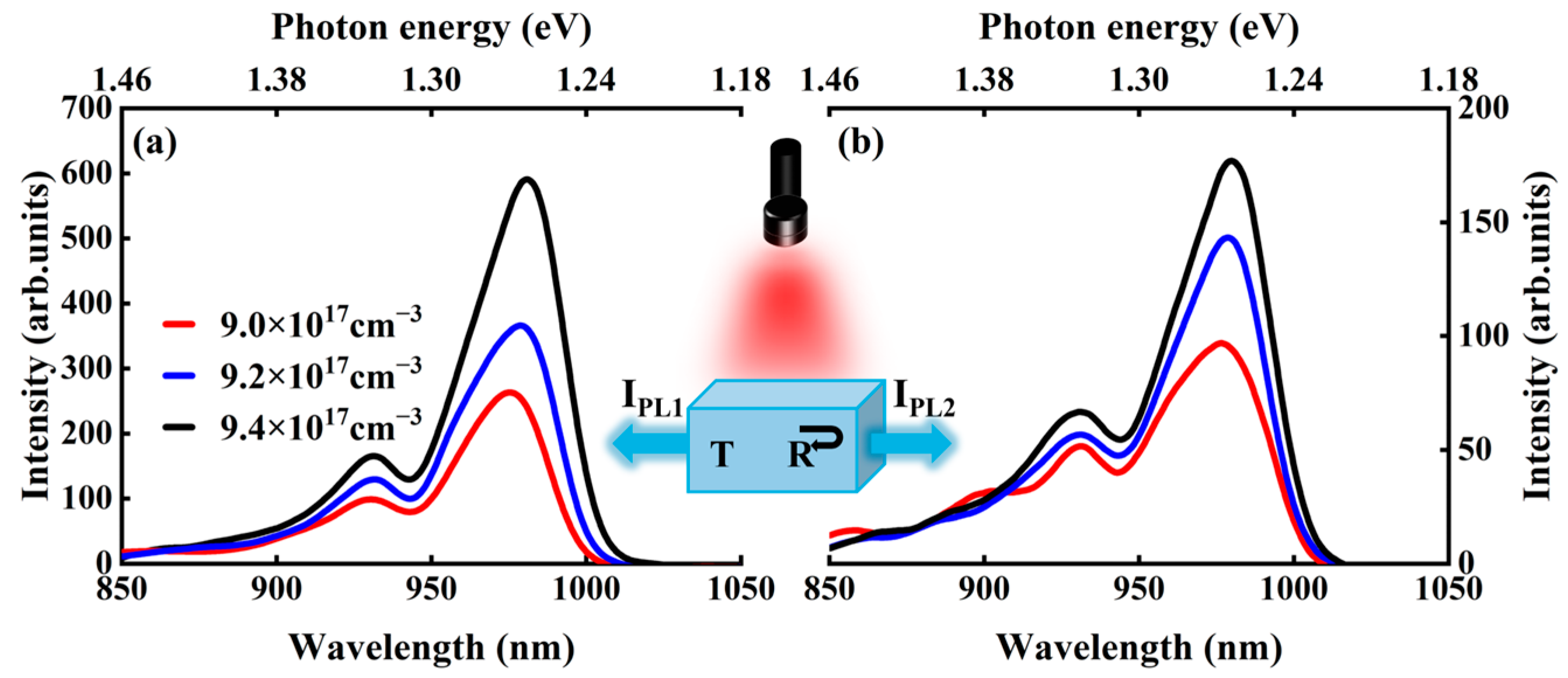
To measure and calculate the carrier inversion factor Pf of the InGaAs/GaAs WIC quantum-confined laser structure, we established an experimental setup to collect the photoluminescence (PL) spectra from the dual facets of the WIC sample, as illustrated in Figure 2. One facet of the sample was coated with an anti-reflectance coating (transmittance T = 99.99%) to eliminate intra-cavity light feedback, while the other facet remained uncoated, with a reflectance R. The epitaxial device was processed in an edge-emitting configuration with an area of 1.5 mm × 3 mm, which was optically pumped by an 808 nm fiber-coupled semiconductor laser with a pulse width of 20 ms (a product of Beijing Laserwave Optoelectronics Technology Co., Ltd. (Beijing, China), Model LWIRL808-40W-F). The PL spectra IPL1 (left) from the coated facet of the device and IPL2 (right) from the uncoated facet are collected by a spectrometer (Ocean Optics Inc. (Dunedin, FL, USA), model HR4000CG-UV-NIR), as shown in Figure 2, where the carrier densities are 9.0 × 10¹⁷ (red), 9.2 × 10¹⁷ (blue), and 9.4 × 10¹⁷ (black) cm−3. The carrier density N can be calculated from the pump power PP by using the following equation [19]:
P P = h ν N W L W A P ( A N + B N 2 + C N 3 ) η a b s
where ηabs is the absorption efficiency of the pump, hν is the photon energy of the 808 nm pumping laser. A, B, and C are the monomolecular, bimolecular, and Auger recombination coefficients. The above parameters for InGaAs material can be found in [19]. AP is the pump spot area, which is designed to be 36 mm2. NW and LW represent the number and thickness of the InGaAs layer, with values of 1 and 10 nm, respectively. The pump powers corresponding to the optically injected carrier densities of 9.0 × 10¹⁷, 9.2 × 10¹⁷, and 9.4 × 1017 cm−3 are 9.8, 10.3, and 10.7 W, respectively.
Unlike the single-peak spectra emitted from classical QW structures, the PL spectra exhibit obvious double-peak characteristics across various carrier densities. This distinctive feature arises from the indium-rich cluster (IRC) effect, which results in the coexistence of multiple active regions with different indium compositions. The multi-peak structure is attributed to emissions from normal and indium-reduced InxGa1−xAs regions. The indium-reduced InxGa1−xAs regions exhibit larger band gaps, forming high-energy localized quantum wells that greatly improve the limiting effect on the photo-generated carriers. This confinement effectively suppresses carrier escape, prolongs carrier lifetime, and significantly enhances radiative recombination efficiency in the short-wavelength region. This greatly improves the carrier inversion level. Additionally, Figure 2 shows that as the carrier concentration increases, the spectral peak (IPL1) shifts slightly from 1.274 to 1.267 eV, and IPL2 moves slightly from 1.272 to 1.268 eV. This shift arises from heat accumulation due to nonradiative recombination, resulting in bandgap shrinkage despite the implementation of a temperature control system [20].

2.3. Experimental Determination of Carrier Distribution

Different from previous experimental methods on carrier inversion factor in semiconductor lasers, this study investigates the carrier distribution properties in WIC structures by analyzing photoluminescence spectra collected from dual facets. According to the definition, the carrier inversion factor Pƒ can be determined as the ratio of modal gain G and spontaneous emission intensity Isp [11]. The value of Pƒ at a particular photon energy, Ehv, reflects the degree of inversion of the states at energies E1 and E2 corresponding to that photon energy (Ehv = E1 − E2) and can be expressed as follows:
P f ( E h v = E 1 E 2 ) = f 1 ( E 1 ) f 2 ( E 2 ) f 1 ( E 1 ) [ 1 f 2 ( E 2 ) ] = K G ( h v ) I s p ( h v )
where the factors f1(E1) and f2(E2) are the occupation probabilities of the upper and lower states, respectively, which participate in the transition at photon energy Ehv = E1 − E2. K denotes the proportional factor. When the energy state is completely occupied by carriers, the corresponding occupancy probability f = 1. Conversely, the occupancy probability f = 0 if the energy state is empty. The inversion factor tends to -∞ at high photon energy, where the upper state is empty and the lower state is full. Conversely, Pf approaches 1 at low photon energies when the system is fully inverted, such that the upper state is completely occupied (f1 = 1) and the lower state is completely empty (f2 = 0). A fully inverted semiconductor system is thus characterized by the inversion factor Pf approaching unity (Pf → 1). Fundamentally, when the carrier distribution is inverted, the occupation probability of the upper energy state E1 exceeds that of the lower energy state E2 (i.e., f1 > f2), resulting in a positive Pf. This population inversion condition is essential for enabling efficient stimulated emission within the material.
The modal gain G and spontaneous emission intensity Isp can be calculated according to the collected PL spectra using the equations [21]:
I P L 1 = I s p G ( e G L 1 ) ( R e G L + 1 )
I P L 2 = I s p G ( 1 R ) ( e G L 1 )
where IPL1 and IPL2 denote the PL intensities measured from the two lateral ends of the WIC sample. L is the distance of light transmitting through the sample in one pass. The facet reflectivity (R ≈ 30%) is mainly determined by the refractive index of the Al0.08–0.15GaAs waveguide layer, since the active layer thickness (10 nm) is much smaller than the waveguide layer thickness (2 μm). The facet reflectivity can be calculated using the following equation:
R = n A l x G a 1 - x A s - n a i r n A l x G a 1 - x A s + n a i r 2
where nair is the air refractive index (~1), and nAlxGa1−xAs represents the refractive index of the waveguide layer, ranging from 3.22 to 3.26. Based on Equation (5), the facet reflectivity is calculated to be R ≈ 0.3.
By combining Equations (3) and (4), the modal gain G can be derived as follows:
G = 1 L ln ( 1 R ) I P L 1 I P L 2 R × I P L 2
The spontaneous emission intensity, Isp can be expressed by substituting (6) into (4):
I s p = R I 2 P L 2 L [ ( 1 R ) 2 I P L 1 ( 1 R 2 ) I P L 2 ] ln ( 1 R ) I P L 1 I P L 2 R × I P L 2
Combining Equations (2), (6), and (7), the carrier inversion factor, Pf can be described as:
P f ( E h v ) = K ( 1 R ) 2 I P L 1 ( 1 R 2 ) I P L 2 R × I 2 P L 2
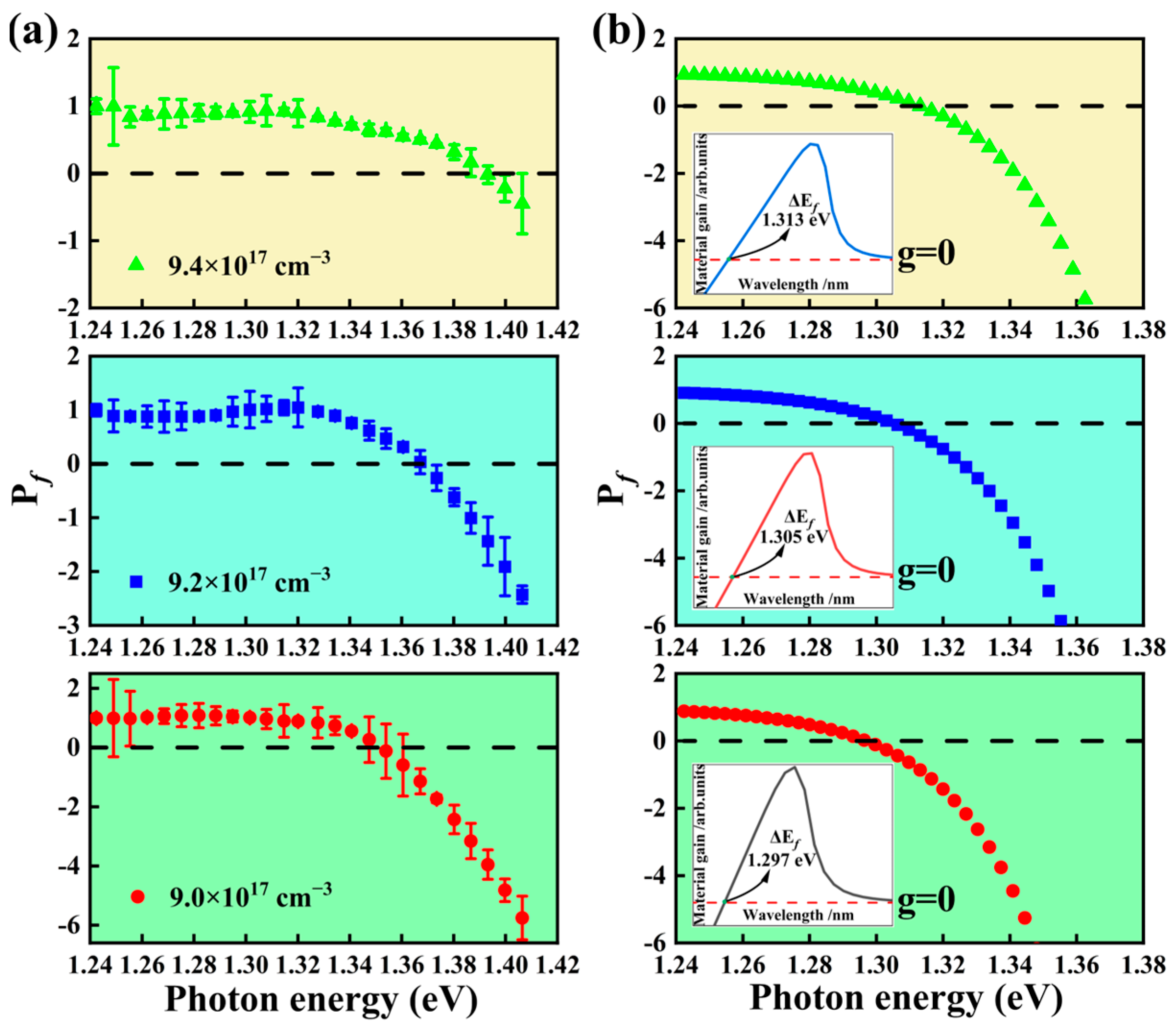
Thus, the carrier inversion factor Pf can be worked out using Equation (8) according to the PL spectra of IPL1 and IPL2 in Figure 2, which represent the intensity at each wavelength. The inversion factor of the WIC structure with the various carrier densities of 9.0 × 10¹⁷, 9.2 × 10¹⁷, and 9.4 × 1017 cm−3 is shown in Figure 3a, where the proportional factor K can be evaluated as about 0.016. The error of Pf at each photon energy was obtained by calculating the absolute difference between the original data and the Savitzky-Golay smoothed data (Polynomial Order: 2, Points of Window: 2 in Origin 2021 software).
To demonstrate the advantages of the WIC structure, the classical QW structure with no IRCs is established by PICS3D, with 10-nm-thick In0.17Ga0.83As material as the well layer, GaAs material as the strain compensation layer of 2 nm thickness, and GaAsP0.08 material with 8 nm thickness as the barrier material. The structural parameters are similar to the WIC structure. The inversion factor (Pf) can be expressed as follows [11]:
P f ( E h v ) = 1 exp E h v Δ E f K B T
where ΔEf is the quasi-Fermi level separation between electrons and holes, KB is the Boltzmann constant, and T is the temperature. The value of ΔEf was determined by simulated material gain spectra (illustration in Figure 3b) by identifying the photon energy at which the material gain g = 0 (transparency point). Therefore, the Pf of the classical QW structure is shown in Figure 3b under similar carrier densities with the corresponding ΔEf of 1.297 eV, 1.305 eV, and 1.313 eV.

3. Results and Discussion

According to (2), the inversion factor Pf depends solely on the occupation probabilities for the upper and lower states of the transition, f1(E1) and f2(E2), respectively. The necessary condition for stimulated emission in semiconductor materials is to achieve the inversion distribution of carriers. Therefore, the carrier’s degree of inversion will directly affect the spectral characteristics of semiconductor materials.
The experimental data for Pf in Figure 3a are unity at low photon energy, corresponding to complete population inversion (f1(E1) = 1, f2(E2) = 0). Regions exhibiting Pf > 0 correspond to the condition where f1(E1) > f2(E2), enabling efficient stimulated emission. Consequently, the energy separation Ehv = E1 − E2 matching the zero-crossing point (Pf = 0) fails to produce effective radiative recombination. This is because E1 and E2 cannot be effectively filled by electrons and holes. Therefore, the energy separation at Pf = 0 can be used to estimate the carrier-filling level. In Figure 3, when the carrier density increases from 9.0 × 10¹⁷ to 9.4 × 1017 cm−3 (4% increase), the band-filling level of the WIC structure increases from 1.352 to 1.392 eV (3.0% enhancement), while that of the classical QW structure increases from 1.297 to 1.313 eV (1.2% enhancement), indicating that WIC structure has higher carrier-filling capacity. Furthermore, compared to classical QW structures, the WIC structure can maintain Pf > 0 at the high-energy side, primarily due to the indium-reduced InGaAs regions, which exhibit the wide band gaps and create the localized high-energy quantum wells. It significantly enhances the probability of carriers occupying high-energy states, enabling effective carrier inversion at the high-energy side. To further investigate the carrier’s degree of inversion, the energy range of carrier inversion distribution (left vertical axis) with Pf > 0 between the special WIC structure and classical QW structure is presented in Figure 4a based on Figure 3. Specifically, the photon energy corresponding to Pf = 0 is first identified from Figure 3, followed by the photon energy 1.24 eV for Pf = 1. The difference between these two energy values is taken as the inversion range shown in Figure 4a. Besides, the ratio (right vertical axis) was also obtained by comparing the inversion ranges between the WIC and QW structures.
Figure 4a clearly shows that the inversion range (0.11, 0.13, and 0.15 eV) of the WIC structure (blue, experimental results) exhibits a broader value compared to that (0.05, 0.06, and 0.07 eV) of the classical QW structure (red, simulation results) under the carrier concentrations of 9.0 × 10¹⁷, 9.2 × 10¹⁷, and 9.4 × 1017 cm−3. The carrier’s degree of inversion in the WIC structure is up to 2.2 times larger than that of the classical QW structure. This indicates a significant increase in the probability of carriers occupying the upper state. Consequently, the WIC structure achieves higher carrier band-filling levels, which leads to the wide spectral bandwidth compared to classical quantum well (QW) structures. For a more comprehensive comparison, the simulated spectra from both WIC and QW structures are shown in Figure 4b. The WIC structure is established by COMSOL Multiphysics software (v6.1), with 4-nm-thick In0.17Ga0.83As, 4-nm-thick In0.12Ga0.88As, and 2-nm-thick In0.15Ga0.85As materials as the active layer, GaAs material as the strain compensation layer of 2 nm thickness, and GaAsP0.08 material with 8 nm thickness as the barrier material. For the QW structure, all layer parameters are identical to those of the WIC structure, except that the active layer consists of 10-nm-thick In0.17Ga0.83As. The results demonstrate that the classical 10-nm In0.17Ga0.83As QW exhibits a single spectral peak with a bandwidth of 42.8 nm, whereas the WIC structure shows two distinct peaks with a broadened bandwidth of 74.8 nm. The WIC structure exhibits higher spectral intensity in the short-wavelength region, indicating that carriers are easier to occupy high-energy levels, resulting in an enhanced Pf. This significantly enhances radiation recombination efficiency in the high-energy side, which is in agreement with our experimental results. This phenomenon is primarily attributed to the coexistence of normal and indium-reduced InxGa1−xAs regions, resulting from the strain-induced migration of indium atoms. The indium-reduced InxGa1−xAs regions, with larger band gaps, make it easier for carriers to occupy the high-energy levels, thereby increasing carrier inversion and band-filling levels, which can greatly expand the spectral bandwidth. To better demonstrate the WIC structure’s advantages in carrier inversion distribution and spectral characteristics, Figure 5 presents theoretically calculated energy band structures for both WIC and QW designs, simulated using COMSOL Multiphysics’ Semiconductor Module with a 2D steady-state drift-diffusion model that incorporates carrier transport, self-consistent potential distribution, and heterojunction boundary conditions. The migration of indium atoms induces nonuniform distributions of indium contents along both the growth and the horizontal directions. This complex distribution feature cannot be precisely represented in band diagrams. Therefore, Figure 5a presents a simplified band model, which simplifies a large number of discrete regions into three regions along the growth direction: In0.17Ga0.83As, In0.12Ga0.88As, and In0.15Ga0.85As to reveal the enhancement mechanism of the carrier inversion factor.
Figure 5a shows the WIC’s band structure with regions of three different band gaps, leading to the improved Fermi distributions of the carriers, which arise due to the IRC effect. Based on our previous study [22], the thicknesses can be evaluated as approximately 4 nm for normal In0.17Ga0.83As and 6 nm for indium-reduced InxGa1−xAs layers. In this paper, the thicknesses of InxGa1−xAs layers with x = 0.17, 0.12, and 0.15 are estimated to be 4, 4, and 2 nm, respectively. The band gap of In0.12Ga0.88As is greater than that of In0.15Ga0.85As, which is larger than that of In0.17Ga0.83As, resulting in step-like sub-bands. These indium-reduced regions exhibit larger band gaps, forming high-energy localized quantum wells. It is beneficial to limit the photo-generated carriers in upper energy states. It improves both the degree of inversion and carrier-injected band-filling ability at high-energy states and then emits high-energy photons to expand the spectral bandwidth. Additionally, the quasi-Fermi levels (Efn and Efp) of electrons and holes are also calculated, which serve as a significant physical parameter in characterizing the carrier-filling level and Fermi-Dirac inversion distribution [23,24,25]. It can be clearly observed that the quasi-Fermi-level separation ΔEf of the WIC structure (0.93 eV) can be as high as 1.09 times that of the classical QW structure (0.85 eV), reflecting the significant advantages of the WIC structure in carrier distribution and gain bandwidth. This implies that carriers are easily transitioned to high-energy states for radiative recombination, thereby improving the effective radiation level spacing and spectral bandwidth. These regions not only increase the probability of carriers occupying high-energy states but also increase the q-Fermi level separation, resulting in an enhanced inversion factor. The improved inversion factor promotes carrier recombination in high-energy states, resulting in a broadened gain bandwidth. The result is of great significance in the development of new types of quantum-confined lasers with wide spectral output. Despite demonstrating promising application potential, this structure remains in the fundamental research stage, requiring further development and rigorous evaluation of its performance under practical application conditions.

4. Conclusions

In this paper, a special InGaAs/GaAs well-island composite (WIC) nanostructure is obtained based on the indium-rich cluster effect during the growth of a highly strained InGaAs/GaAs material system. The inversion factor of the optically pumped InxGa1−xAs WIC structure is obtained according to the photoluminescence (PL) spectra collected from both ends of the WIC epitaxial device. The analysis of carrier distribution data reveals that the degree of inversion in the WIC structure can be up to 2.2 times higher than in classical QW structures over the same carrier concentration range of 9.0 × 10¹⁷ to 9.4 × 1017 cm−3. Additionally, the simulated spectra and band structure demonstrate that the WIC structure exhibits a higher quasi-Fermi-level separation and carrier-filling level. This suggests that carriers are more easily inverted into high-energy states, which in turn facilitates the emission of spectra with a broader bandwidth. The findings of this research are of significant importance for the development of next-generation quantum-confined lasers with wide spectral outputs.

Author Contributions

Conceptualization, X.G.; methodology, Z.C. and K.M.; software, R.W.; validation, Q.Y.; formal analysis, Z.J. and X.Q.; investigation, W.W.; resources, W.W.; data curation, H.L.; writing—original draft preparation, X.G.; writing—review and editing, J.W.; visualization, G.L.; supervision, Q.Y.; project administration, X.G.; funding acquisition, J.W. All authors have read and agreed to the published version of the manuscript.

Funding

This research was funded by the National Natural Science Foundation of China, grant number 62204172, the innovative Leading Talents in the Universities of Xishan Talents Program, grant number 2023xsyc002, the basic science (Natural science) research project of higher education in Jiangsu Province, grant number 22KJB140016, the Wuxi University research start-up fund for introduced talents, grant number 550221009, and the Wuxi “Taihu Light” Science and Technology Research Plan, grant number K20241049.

Institutional Review Board Statement

Not applicable.

Informed Consent Statement

Not applicable.

Data Availability Statement

The data underlying the results presented in this paper are not publicly available at this time; however, they may be obtained from the authors upon reasonable request.

Acknowledgments

The authors acknowledge the support of the School of Electronic Information Engineering, Wuxi University.

Conflicts of Interest

The authors declare no conflicts of interest.

Abbreviations

The following abbreviations are used in this manuscript:
WICwell-island composite
TEInTrimethylindium
TMGatrimethylgallium
SOAssemiconductor optical amplifiers
PLphotoluminescence
IRCIndium-rich cluster
QWquantum well
MOCVDmetal-organic chemical vapor deposition

References

  1. Rodrigues, L.N.; Scolfaro, D.; da Conceição, L.; Malachias, A.; Couto, O.D.D., Jr.; Iikawa, F.; Deneke, C. Rolled-Up Quantum Wells Composed of Nanolayered InGaAs/GaAs Heterostructures as Optical Materials for Quantum Information Technology. ACS Appl. Nano Mater. 2021, 4, 3140–3147. [Google Scholar] [CrossRef]
  2. Liu, H.; Wang, J.; Guo, D.; Shen, K.; Chen, B.; Wu, J. Design and fabrication of high performance InGaAs near infrared photodetector. Nanomaterials 2023, 13, 2895. [Google Scholar] [CrossRef] [PubMed]
  3. Zubov, F.; Maximov, M.; Kryzhanovskaya, N.; Moiseev, E.; Muretova, M.; Mozharov, A.; Kaluzhnyy, N.; Mintairov, S.; Kulagina, M.; Ledentsov, N.; et al. High speed data transmission using directly modulated microdisk lasers based on InGaAs/GaAs quantum well-dots. Opt. Lett. 2019, 44, 5442–5445. [Google Scholar] [CrossRef] [PubMed]
  4. Yu, H.; Wang, M.; Zhou, D.; Zhou, X.; Wang, P.; Liang, S.; Zhang, Y.; Pan, J.; Wang, W. A 1.6-μm widely tunable distributed Bragg reflector laser diode based on InGaAs/InGaAsP quantum-wells material. Opt. Commun. 2021, 497, 127201. [Google Scholar] [CrossRef]
  5. Kaur, P.; Buttar, A.S.; Raj, B. Analytical modeling and performance assessment of high performance split-gate dielectric modulated InGaAs GAA junctionless MOSFET biosensor. Micro Nanostruct. 2022, 171, 207395. [Google Scholar] [CrossRef]
  6. Zheng, M.; Yu, Q.; Li, X.; Tai, H.; Zhang, X.; Zhang, J.; Ning, Y.; Wu, J. Ultrabroadband and independent polarization of optical amplification with InGaAs-based indium-rich cluster quantum-confined structure. Appl. Phys. Lett. 2020, 116, 252106. [Google Scholar] [CrossRef]
  7. Yu, Q.; Zheng, M.; Tai, H.; Lu, W.; Shi, Y.; Yue, J.; Zhang, X.; Ning, Y.; Wu, J. Quantum Confined Indium-Rich Cluster Lasers with Polarized Dual-Wavelength Output. ACS Photonics 2019, 6, 1990–1995. [Google Scholar] [CrossRef]
  8. Schlenker, D.; Miyamoto, T.; Chen, Z.; Koyama, F.; Iga, K. Growth of highly strained GaInAs/GaAs quantum wells for 1.2 μm wavelength lasers. J. Cryst. Growth 2000, 209, 27–36. [Google Scholar] [CrossRef]
  9. Jasik, A.; Wnuk, A.; Wójcik-Jedlińska, A.; Jakieła, R.; Muszalski, J.; Strupiński, W.; Bugajski, M. The influence of the growth temperature and interruption time on the crystal quality of InGaAs/GaAs QW structures grown by MBE and MOCVD methods. J. Cryst. Growth 2008, 310, 2785–2792. [Google Scholar] [CrossRef]
  10. Yu, H.; Roberts, C.; Murray, R. Influence of indium segregation on the emission from InGaAs/GaAs quantum wells. Appl. Phys. Lett. 1995, 66, 2253. [Google Scholar] [CrossRef]
  11. Thomas, R.; Smowton, P.M.; Blood, P. Radiative recombination rate measurement by the optically pumped variable stripe length method. Opt. Express 2015, 23, 3308–3315. [Google Scholar] [CrossRef]
  12. Duffy, D.A.; Marko, I.P.; Fuchs, C.; Stolz, W.; Sweeney, S.J. The impact of band bending on the thermal behaviour of gain in type-II GaAs-based “W”-lasers. IEEE J. Sel. Top. Quantum Electron. 2024, 31, 1–10. [Google Scholar] [CrossRef]
  13. Thomson, J.D.; Smowton, P.M.; Blood, P.; Klem, J.F. Optical gain and spontaneous emission in GaAsSb–InGaAs Type-II “W” laser structures. IEEE J. Quantum Electron. 2007, 43, 607–613. [Google Scholar] [CrossRef]
  14. Egorov, S.V.; Petrov, A.G.; Baranov, A.N.; Zakhar’in, A.O.; Andrianov, A.V. On feasibility of population inversion between the quantum confinement levels in quantum wells under interband photoexcitation. J. Infrared Milli Terahz Waves 2021, 42, 986–1004. [Google Scholar] [CrossRef]
  15. Wenzel, H.; Kantner, M.; Radziunas, M.; Bandelow, U. Semiconductor Laser Linewidth Theory Revisited. Appl. Sci. 2021, 11, 6004. [Google Scholar] [CrossRef]
  16. Qiu, Y.-Q.; Lvr, Z.-R.; Wang, H.; Wang, H.-M.; Yang, X.-G.; Yang, T. Improved linewidth enhancement factor of 1.3-µm InAs/GaAs quantum dot lasers by direct Si doping. AIP Adv. 2021, 11, 055002. [Google Scholar] [CrossRef]
  17. Muraki, K.; Fukatsu, S.; Shiraki, Y.; Ito, R. Surface segregation of In atoms during molecular beam epitaxy and its influence on the energy levels in InGaAs/GaAs quantum wells. Appl. Phys. Lett. 1992, 61, 557–559. [Google Scholar] [CrossRef]
  18. Ruterana, P.; Singh, P.; Kret, S.; Cho, H.K.; Lee, H.J.; Suh, E.K.; Jurczak, G.; Maciejewski, G.; Dluzewski, P. Size and shape of In rich clusters and InGaN QWs at the nanometer scale. Phys. Status Solidi C 2005, 2, 2381–2384. [Google Scholar] [CrossRef]
  19. Kuznetsov, M.; Hakimi, F.; Sprague, R.; Mooradian, A. Design and characteristics of high-power (>0.5-W CW) diode-pumped vertical-external-cavity surface-emitting semiconductor lasers with circular TEM beams. IEEE J. Sel. Top. Quantum Electron. 1999, 5, 561–573. [Google Scholar] [CrossRef]
  20. Paul, S.; Roy, J.B.; Basu, P.K. Empirical expressions for the alloy composition and temperature dependence of the band gap and intrinsic carrier density in GaxIn1−xAs. J. Appl. Phys. 1991, 69, 827–829. [Google Scholar] [CrossRef]
  21. Ma, M.-L.; Wu, J.; Ning, Y.-Q.; Zhou, F.; Yang, M.; Zhang, X.; Zhang, J.; Shang, G.-Y. Measurement of gain characteristics of semiconductor lasers by amplified spontaneous emissions from dual facets. Opt. Express 2013, 21, 10335. [Google Scholar] [CrossRef]
  22. Kong, Y.; Ma, R.; Shen, B.; Yu, Q. Experimental Detection on Thickness Fluctuation of InxGa1-xAs-Based Indium-Rich Cluster Structure. IEEE Photonics J. 2022, 14, 1–4. [Google Scholar] [CrossRef]
  23. Lee, J.; Yeo, H.; Kim, Y.-H. Quasi-Fermi level splitting in nanoscale junctions from ab initio. Proc. Natl. Acad. Sci. USA 2020, 117, 10142–10148. [Google Scholar] [CrossRef] [PubMed]
  24. Wu, L. Accurate determination of quasi-Fermi-level separation of semiconductor lasers. Appl. Phys. Lett. 2000, 76, 964–966. [Google Scholar] [CrossRef]
  25. Li, D.; Feng, L.; Yang, W.; Yang, X.; Hu, X.; Wang, C. Redefinition the quasi-Fermi energy levels separation of electrons and holes inside and outside quantum wells of GaN based multi-quantum-well semiconductor laser diodes. J. Phys. D Appl. Phys. 2020, 53, 155104. [Google Scholar] [CrossRef]
Figure 1. Formation mechanism and morphology characterization of the InGaAs well-island composite nanostructure. (a) InGaAs well-island composite structure. (b) Formation mechanism of the WIC nanostructure. (c) AFM photographs of IRCs.
Photonics 12 00834 g001
Figure 2. Experimental setup and PL spectra measured from dual facets with the carrier densities of 9.0 × 10¹⁷, 9.2 × 10¹⁷, and 9.4 × 1017 cm−3. (a) The PL spectra IPL1 (left) measured from the coated facet. (b) The PL spectra IPL2 (right) measured from the uncoated facet.
Photonics 12 00834 g002
Figure 3. The carrier inversion factor Pf obtained from the WIC structure and the classical QW structure with the carrier concentrations of 9.0 × 10¹⁷~9.4 × 1017 cm−3 at 300 K, respectively. (a) The experimental result of the WIC structure. (b) The Pf and material gain of the classical QW structure simulated by PICS3D.
Photonics 12 00834 g003
Figure 4. Energy range of carrier inversion distribution and simulated spectra. (a) The inversion range and ratio of the WIC structure and the QW structure. (b) Simulated spectra from the WIC structure and the QW structure.
Photonics 12 00834 g004
Figure 5. Simulated energy band structures of the WIC structure and classical QW structure under the same conditions. (a) The InGaAs-based WIC structure. (b) The classical QW structure with a thickness of 10 nm.
Photonics 12 00834 g005
Disclaimer/Publisher’s Note: The statements, opinions and data contained in all publications are solely those of the individual author(s) and contributor(s) and not of MDPI and/or the editor(s). MDPI and/or the editor(s) disclaim responsibility for any injury to people or property resulting from any ideas, methods, instructions or products referred to in the content.