1. Introduction
The massive data transmission demands driven by the large-scale commercialization of 5G pose significant challenges to the transmission capacity of existing fiber-optic communication systems [
1,
2]. The Nyquist wavelength division multiplexing (WDM) system is a potential solution to enable large-capacity optical transmission. However, the orthogonal transmission rule limits the system from further improving spectral efficiency (SE), so it is still difficult for Nyquist WDM systems to meet the development needs for future high-SE and large-capacity optical transmission systems. Faster-than-Nyquist (FTN) technology compresses the signal spectrum through digital domain or electrical domain tight filtering, making the symbol rate greater than the channel spacing and introducing controlled inter-symbol-interference (ISI), which theoretically provides higher spectral efficiency compared to Nyquist [
3,
4].
In the FTN-WDM system with a high symbol rate and high modulation format, the code pattern of the high modulation format could significantly reduce the Euclidean distance. Moreover, FTN tight filtering will introduce serious ISI, which will make the system more sensitive to receiver (Rx) IQ imbalance impairments at the receiver, such as amplitude imbalance (Amp. Imb.), phase imbalance (Pha. Imb.), and timing misalignment (skew). Meanwhile, Rx IQ imbalance and ISI impairments will make the timing recovery algorithm need a greater convergence cost to establish the timing synchronization loop. Currently, mainstream Rx IQ imbalance compensation schemes are categorized into time domain and frequency domain. The conventional scheme in the time domain is the Gram–Schmidt orthogonalization procedure (GSOP) [
5]. However, the GSOP algorithm needs parallel computation in the actual system, so the computational complexity is relatively high. In [
6], the authors proposed that the blind time domain (BTD) 4 × 4 equalizer could effectively compensate for the Rx IQ imbalance, but this algorithm did not take into account the IQ crosstalk caused by dispersion compensation during long-distance transmission, resulting in a decline in the IQ imbalance compensation effect. In [
7], the authors proposed a combined chromatic dispersion (CD) compensation and BTD 4 × 2 equalization algorithm to achieve Rx IQ imbalance compensation under long-distance transmission. However, the aforementioned Rx IQ imbalance compensation schemes, which are implemented in the time domain, suffer from relatively high computational complexity. The frequency domain IQ imbalance compensation schemes reported in the literature are as follows. In [
8], the authors proposed the Rx IQ imbalance compensation of a blind frequency domain (BFD) 4 × 2 equalizer based on the constant modulus algorithm (CMA). In [
9], a frequency-domain widely linear 2 × 2 multiple-input multiple-output (MIMO) equalizer scheme was proposed. However, these equalization algorithms are not applicable to higher-order modulation formats [
10,
11]. In [
12], the authors proposed a 4 × 2 MIMO frequency domain equalizer based on the radius directed equalization (RDE) algorithm that could compensate for the Rx IQ imbalance impairment in coherent optical transmission systems with a high-order modulation format. However, due to the severe ISI impairment inherent in the FTN system, the compensation performance of the Rx IQ imbalance schemes reported in the aforementioned literature will deteriorate. On the other hand, in response to the problem of Rx IQ imbalance, this impairment makes it difficult for the timing recovery algorithm to work properly. In [
13], the authors propose a joint scheme of Rx IQ skew compensation and timing recovery in the frequency domain, which could effectively compensate for Rx IQ skew and sample clock offset (SCO). However, in the FTN system, it is inherently challenging to achieve timing recovery in the frequency domain, rendering this scheme impractical for the FTN system. In [
14], the authors propose the squared Gardner phase detector (SGPD) timing recovery algorithm, which could stably establish a timing synchronization loop in FTN systems and requires sampling only twice. In [
15], the authors proposed a pilot-based timing recovery algorithm with greater tolerance for differential group delay (DGD), Rx IQ imbalance, and other impairments. However, the above algorithm does not consider the problems of increased convergence cost required to establish the timing synchronization loop caused by IQ imbalance and ISI impairments.
In this paper, we propose a joint scheme of Rx IQ imbalance and timing recovery to solve the above problems. First, the proposed scheme employs a decision-directed least mean square (DDLMS) algorithm to perform preliminary ISI equalization, thereby mitigating the impact of severe ISI impairments induced by aggressive FTN filtering on the compensation of Rx IQ imbalance. Simultaneously, by embedding a two-stage Rx IQ imbalance compensation algorithm into the timing recovery feedback loop, the scheme equalizes part of the ISI and IQ imbalance impairments in the FTN signal, thereby reducing the convergence cost required for the timing recovery algorithm to establish stable timing synchronization.
2. Principle of the Proposed Scheme
To simplify the analytical model, consider the X-pol of the FTN 16-quadrature amplitude modulation (QAM) signal as an example. Under Rx IQ imbalance impairments, the received signal could be expressed as
Table 1 consolidates notations recurring across Equations (1) and (2).
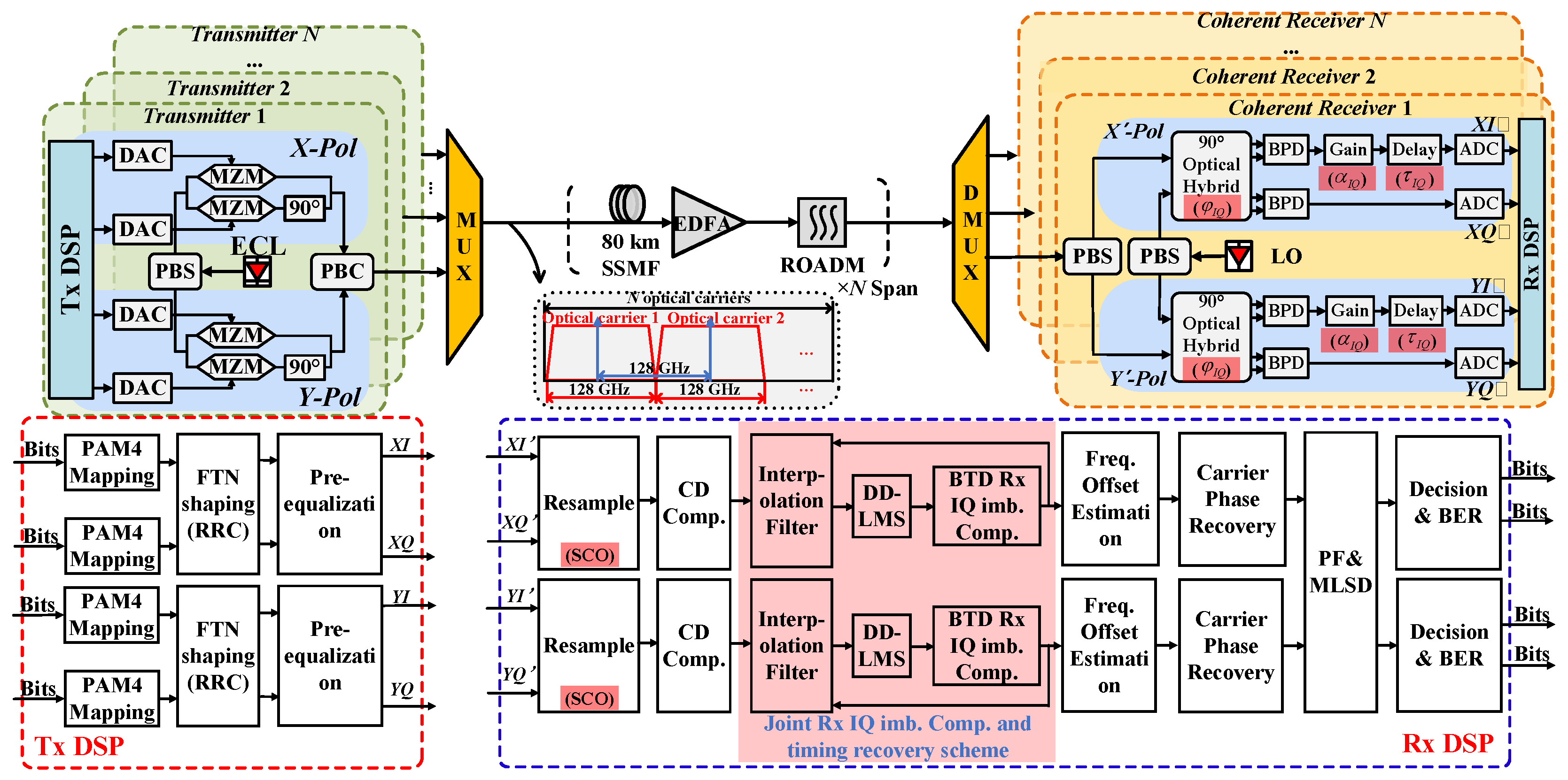
As evident from Equation (1), the impulse response of the FTN shaping filter introduces severe ISI impairments when the acceleration factor is reduced. These impairments not only degrade the equalization efficacy of traditional Rx IQ imbalance compensation algorithms but also increase the convergence cost required for the SGPD timing recovery algorithm to establish a timing synchronization loop. Therefore, it is critical to mitigate the ISI impairment on Rx IQ imbalance compensation algorithms in FTN systems. However, when a significant sample clock offset (SCO) exists, the phase and amplitude deviations in the sampled values at the receiver degrade the performance of Rx IQ imbalance compensation algorithms based on time domain/frequency domain adaptive equalization and polarization demultiplexing. This results in mutual constraints between IQ imbalance compensation and the timing recovery algorithm. To enable coordinated and complementary operation between the Rx IQ imbalance compensation and timing recovery algorithms, we propose a joint Rx IQ imbalance and timing recovery scheme, as shown in
Figure 1.
The proposed scheme includes the following two main points.
- (i)
ISI and Rx IQ imbalance are compensated in the timing recovery feedback loop.
The asynchronously sampled FTN signals are first processed through CD compensation and then fed into a timing synchronization loop embedded with a two-stage Rx IQ imbalance compensation module, which comprises a DDLMS algorithm and a BTD 4 × 2 equalizer. First, the DDLMS equalizer performs preliminary ISI equalization on the CD-compensated asynchronous samples to mitigate the severe ISI distortions caused by the FTN shaping filter, thereby reducing their adverse impact on the subsequent second-stage Rx IQ imbalance compensation. This is because sample clock errors and Rx IQ imbalance impairments interact with each other, resulting in the limited performance of the DDLMS algorithm in equalizing ISI. Subsequently, the BTD 4 × 2 equalizer monitors and compensates for Rx IQ imbalance while simultaneously achieving polarization demultiplexing and adaptive equalization. The output of the BTD 4 × 2 equalizer is given by Equation (3).
The error calculation formula is shown in Equation (4).
where
RR denotes the radius of the ideal signal. When the modulation format is 16-QAM,
RR is
,
, and
. The tap coefficients update process of the equalizer could be formulated as follows:
In the above equation,
denotes the iteration step size;
conj denotes the conjugate. In the proposed joint scheme, an excessively large iteration step size
accelerates initial convergence but compromises precise convergence to the global optimum, thereby degrading performance and potentially causing algorithmic divergence. Conversely, an undersized step size enhances convergence accuracy at the expense of prohibitively high computational overhead due to excessive iterations. In conclusion, a reasonable initial iteration compensation value needs to be set to achieve the optimal performance of the proposed algorithm. When the BTD 4 × 2 equalizer converges, the tap coefficient matrix is reciprocal with the Rx IQ imbalance impairment matrix. The Rx IQ imbalance impairment matrix could be expressed as follows:
Table 2 consolidates notations recurring across Equation (7).
Based on the BTD 4 × 2 equalizer, the tap coefficient matrix could be expressed as
Using Equation (8), the Rx IQ phase imbalance, amplitude imbalance, and skew could be calculated as
- (ii)
Timing recovery in the feedback loop.
Within the feedback loop, the two-stage Rx IQ imbalance compensation algorithm mitigates IQ imbalance, ISI, and DGD. The equalized samples are then fed into the timing error detector (TED) module of the SGPD to compute timing errors. The SGPD TED formula is given by
The calculated timing error is subsequently fed into the loop filter, which generates the control word W based on the TED output. The loop filter consists of a proportional unit and an integral unit. The proportional unit tracks the timing phase difference, while the integral unit tracks the timing frequency difference. Using the control word, the control unit calculates the base pointer and fractional interval, which guide the interpolation filter to resample the multiplexed signal. This completes the processing of a set of asynchronous samples by the timing synchronization loop. For clock feedback synchronization loops, the TED only needs to provide the error direction. The resampled multiplexed signal sequence is then processed iteratively by the clock synchronization loop through the aforementioned steps. The interpolation filter continuously adjusts the timing error for subsequent asynchronous sample sequences based on feedback, enabling persistent tracking and correction. This cyclic process continues until the fractional interval evolves from random fluctuations into a stable periodic pattern. At this stage, the clock synchronization loop achieves lock, outputting a synchronized carrier signal sample sequence. Let the RMS value of the timing error detection be expressed as [
16]
In the above equation, NRMS denotes the block length for the RMS calculation, and represents the timing detection error.
3. Complexity Analysis and Comparison
As shown by
Figure 1, the joint scheme Rx IQ imbalance compensation and timing recovery scheme includes the following parts.
① The two-stage receiver IQ imbalance compensation algorithm. The first level, the DDLMS algorithm, requires 4NDD real-number multiplication for each symbol. NDD is the tap length of the DDLMS algorithm. The second level, a BTD 4 × 2 equalizer, requires 32NBTD + 96 real-number multiplication. NBTD indicates the tap length of the BTD 4 × 2 algorithm.
② The timing synchronization feedback loop of the SGPD timing recovery algorithm mainly includes four parts: timing error detector, loop filter, control unit, and interpolation filter. Among them, the timing error detector part requires seven real-number multiplications per symbol. The loop filter requires four multiplications of real numbers per symbol. In the control unit, the output of the numerically controlled oscillator (NCO) is and the fractional interval is , so each symbol requires four real multiplications. The interpolation filter uses the Lagrange square interpolation method to match the received asynchronous sampling sequence, obtain continuous curves according to the Lagrange interpolation formula, and resample the sequence after synchronization. When calculating the interpolation coefficient and the interpolated output, 96 real multiplications are required for each symbol. To sum up, a total of 111 real multiplications are required for each symbol in the timing recovery feedback loop.
The Rx IQ imbalance and timing recovery computational complexity of the two schemes are shown in
Table 3.
The implementation complexity per symbol is evaluated in a 128 GBaud PM-16QAM FTN scheme under 0.9 AF.
NBFD indicates the tap length of the conventional BFD algorithm in
Table 1. Assuming that
NBTD and
NBFD are 25, the above parameters are put into the table, and it can be concluded that each symbol in the proposed scheme requires 1007 real number multiplications, and the conventional BFD scheme requires 777 real number multiplications. Based on the above analysis, the computational complexity of the proposed scheme increases by about 29.6% compared with the conventional BFD scheme. However, the proposed scheme could compensate for the Rx IQ imbalance impairment after ISI compensation for FTN signals, so the proposed scheme has better Rx IQ imbalance compensation performance than the conventional BFD scheme.
4. Simulation and Discussions
As illustrated in
Figure 2, a 128 Gbaud PM 16-QAM FTN-WDM coherent optical transmission system was constructed using VPI and Optilux to validate the performance of the proposed scheme. In the simulation platform, the Rx IQ imbalance and sample clock offset (SCO) impairments were introduced as follows: Rx IQ amplitude imbalance was generated by applying unequal amplification to the electrical signals of the I components in the X-polarization and Y-polarization. Rx IQ skew was introduced by applying time delays to the XI and YI signals, while Rx IQ phase imbalance was emulated using a 90° optical hybrid. Additionally, since the VPI 9.9 simulation software could not introduce SCO impairment, this impairment was incorporated through a resampling algorithm in the Rx DSP.
Under 128 GBaud PM 16-QAM FTN 0.9 AF and back-to-back (BTB) transmission conditions, simulations were conducted to evaluate the Q-factor variation with Rx IQ imbalance impairments. Through exhaustive parameter optimization, an initial step size of 0.0005 is identified as optimal for the joint compensation algorithm. As shown in
Figure 3, the Q-factor variations with respect to Rx IQ amplitude imbalance, Rx IQ phase imbalance, and Rx IQ skew are demonstrated for the proposed scheme, conventional BFD scheme, and BTD 2 × 2 MIMO algorithm, respectively. The BTD 2 × 2 MIMO algorithm adopts a butterfly-structured adaptive filter, where the inputs and outputs correspond to the sampled signals of the two polarization states. As evidenced by the simulation results, the proposed scheme achieves a 0.25 dB improvement in Q-factor compared to the conventional BFD scheme. Furthermore, the Q-factor remains nearly constant with increasing Rx IQ imbalance for both the proposed scheme and the conventional BFD scheme. Additionally, under a Q-penalty threshold of 0.1 dB, the proposed scheme and the conventional BFD scheme achieve compensation ranges of [−8, 8] dB and [−7, 7] dB for Rx IQ amplitude imbalance, [−45, 45] deg and [−40, 40] deg for Rx IQ phase imbalance, and [−7, 7] ps and [−6, 6] ps for Rx IQ skew, respectively. This corresponds to 14%, 12.5%, and 16.6% improvements in Rx IQ amplitude, phase, and skew compensation ranges for the proposed scheme compared to the conventional BFD scheme. This improvement primarily stems from the DDLMS algorithm in the proposed scheme, which equalizes partial ISI impairments prior to compensating for Rx IQ imbalance, thereby enhancing the compensation efficacy of the Rx IQ imbalance algorithm. In contrast, when employing the BTD 2 × 2 MIMO algorithm, the Q-factor exhibits severe degradation with increasing Rx IQ imbalance. Specifically, at 1.6 dB amplitude imbalance, 8.5 deg phase imbalance, and 1 ps IQ skew, the system incurs a Q-penalty of 1 dB.
In the presence of Rx IQ imbalance, simulations were conducted to validate the estimation accuracy of the proposed scheme. As shown in
Figure 4, the simulation results demonstrate that the proposed scheme achieves an estimation accuracy of approximately 0.14 dB for Rx IQ amplitude imbalance within the range of [−8, 8] dB, 0.3 deg for phase imbalance within [−45, 45] deg, and 0.2ps for IQ skew within [−7, 7] ps. The estimated accuracy of the proposed scheme fluctuates with the variation in Rx IQ imbalance, mainly due to the influence of random noise in the simulation system. Additionally, the proposed scheme continuously approaches the minimum cost function by adjusting the iterative compensation, but the accuracy of the iterative step size is always limited, which is also a cause of the variation in estimation accuracy.
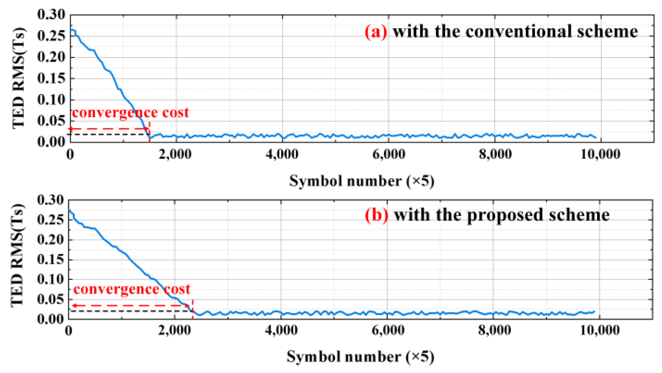
Figure 5 shows a comparison of the convergence costs required to establish the timing synchronization loop using the different schemes under a 128 GBaud PM-16QAM FTN system with 0.9 AF. The specific simulation conditions are SCO of 200 ppm, 240 km transmission fiber, and Rx IQ skew, amplitude imbalance, and phase imbalance of 5 ps, 2 dB, and 20 deg, respectively. This paper adopts the conclusion of Ref. [
16], i.e., when RMS is about 0.02 Ts, it indicates that the timing recovery algorithm could realize timing synchronization. The conventional BFD scheme is described above, which consists of a BFD 4 × 2 MIMO equalization algorithm and an SGPD timing recovery algorithm. It could be seen from the simulation results that the RMS curves of both the conventional BFD scheme and the proposed scheme could converge stably to about 0.02 Ts/0.019 Ts, respectively, indicating that both schemes could complete clock synchronization under the FTN system. At the same time, it could be seen that the convergence cost required to establish a timing synchronization loop using the proposed scheme is reduced by about 42% compared to the conventional BFD scheme. The main reasons are as follows. On the one hand, the proposed scheme equalized part of the ISI impairment in advance through the DDLMS algorithm, so that the proposed scheme could better compensate for the IQ imbalanced impairment at the receiving end. On the other hand, the receiver IQ compensation algorithm embedded in the timing synchronization loop equalizes the receiver IQ imbalance, DGD, ISI, and other impairments before calculating the timing error, thus effectively reducing the convergence cost required by the timing recovery algorithm to establish the timing synchronization loop.
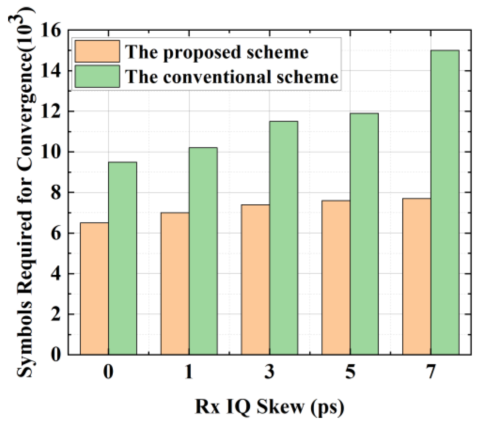
As shown in
Figure 6, the convergence costs required to establish the timing synchronization loop using the proposed scheme and the conventional BFD scheme under the condition of different Rx IQ skew are compared. The specific simulation conditions are SCO of 200 ppm, transmission of 240 km, and amplitude imbalance and phase imbalance of 2 dB and 20 deg, respectively. The convergence cost required for the establishment of the timing synchronization loop in
Figure 6 is determined by averaging the convergence cost after multiple simulations, where RMS values stabilize in less than 0.02 Ts. The simulation results show that in the [0, 5] ps range, where both schemes work stably, the convergence cost of the conventional BFD scheme increases faster with the increase in Rx IQ skew than that of the proposed scheme. This is because, compared with the conventional BFD scheme, the proposed scheme could balance part of the ISI impairment before compensating for the Rx IQ imbalance, so it has a better IQ imbalance compensation effect, which reduces the impact of IQ imbalance, ISI, DGD, and other impairments before timing error calculation. In addition, in the IQ skew range where both schemes work stably, the proposed scheme could reduce the convergence cost by at least 31% compared with the conventional BFD scheme. When the receiver IQ skew is 7 ps, the convergence cost of the proposed scheme is about 50% lower than that of the conventional BFD scheme because it is difficult to stably compensate for the Rx IQ skew.
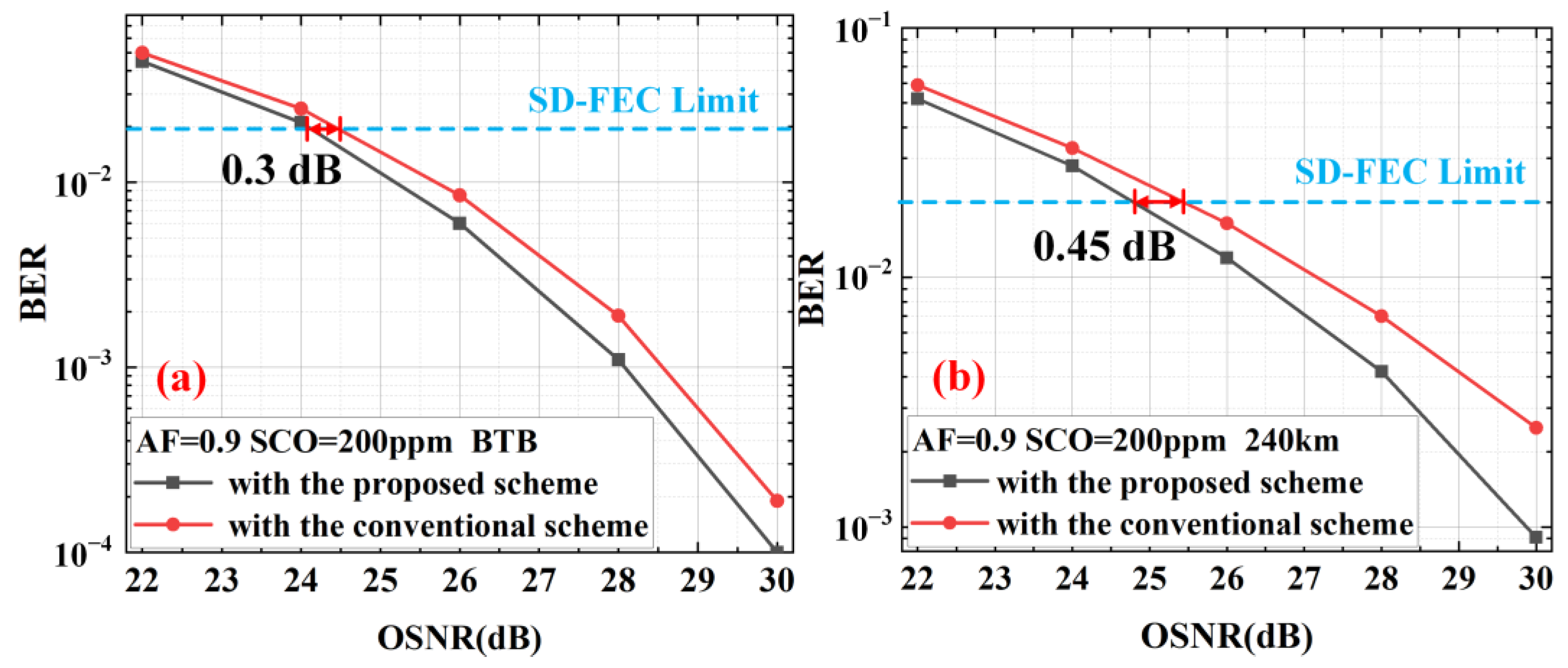
As can be seen from
Figure 7, under the conditions of BTB transmission, SCO of 200 ppm, and Rx IQ skew, amplitude imbalance, and phase imbalance of 5 ps, 2 dB, and 20 deg, respectively, compared with the conventional BFD scheme, the proposed scheme has an OSNR tolerance of about 0.3 dB (@128 GBaud PM-16QAM BER = 2 × 10
−2). In addition, the proposed scheme has an OSNR tolerance of about 0.45 dB (@128GBaud PM-16QAM BER = 2 × 10
−2) compared with the conventional BFD scheme when transmitting 240 km.
5. Experimental Setup and Performance Analysis
Performance evaluation of the proposed scheme employed 40 GBaud PM-16QAM FTN-WDM experiments. The transmitter’s offline DSP implemented FTN shaping via a root-raised cosine (RRC) filter (manufactured by Finisar Corporation (subsidiary in Wuxi, China), and laboratory instruments were procured from Finisar China). Discrete samples underwent pre-equalization post-shaping to mitigate high-frequency impairment before being fed into an Agilent 8194A arbitrary waveform generator (AWG) (produced by Agilent Technologies (headquartered in Santa Clara, CA, USA), with the laboratory unit purchased through Keysight Distributor (China)). Operating at 120 Gsample/s with ∼45 GHz −3 dB bandwidth, the AWG synchronized four channels. Three-fold oversampling generated 40 GBaud electrical signals. Three tunable external cavity lasers (ECLs), emitting carriers at ∼50 kHz linewidth and spaced at 40 GHz around 193.414 THz, were partitioned into odd/even channel groups. These drove dual-polarization IQ modulators (modulator 1 and 2) (originated from Rayley Corporation (Shenzhen, China), and the laboratory modulator was acquired domestically in China) with AWG-generated I/Q electrical signals. Modulated carriers entered a recirculating fiber loop comprising optical couplers, optical switch (OS), optical bandpass filter (OBPF), and 80 km G.652D SSMF spans (0.17 dB/km attenuation, 0.2 ps/km1/2 PMD) with EDFA amplification. OBPF1 completes the out-of-band noise filtering for each span, while launch power was maintained at 4 dBm to suppress nonlinearities. After fiber loop transmission, PM-16QAM FTN signals are passed through an OBPF2. A Lecroy 10Zi-A real-time oscilloscope (80 Gsample/s, 30 GHz −3 dB bandwidth) (manufactured by Teledyne LeCroy (Chestnut Ridge, NY, USA), with the laboratory device sourced via Keysight Distributor (China)) sampled the PM-16QAM FTN waveforms for offline processing. Receiver DSP sequentially executed: resampling, chromatic dispersion compensation, the joint compensation scheme, frequency offset correction, carrier phase recovery, post-filter with maximum-likelihood sequence detection (PF-MLSD), and BER calculation.
In the offline experiment platform, IQ skew and IQ amplitude imbalance impairments were introduced by sampling an oscilloscope. By using the built-in “deskew” function of the oscilloscope, the time offset of XI and YI waveform samples is adjusted by inputting a specific delay, so as to achieve the setting of Rx IQ skew; the setting range is [−25, 25] ns. In addition, the “Rescale” function of the oscilloscope is used to achieve the unbalanced setting of Rx IQ amplitude, and the peak-to-peak value of single-channel output voltage does not exceed 2 V. The function of the “Rescale” function is y = ax + b, where a and b are the multiplication and addition coefficients, respectively; x is the channel sampling value; and y is the output sampling value. The Rx IQ Amp. Imb between XQ and YQ is formed by changing the XI and YI amplitudes. Since the IQ phase imbalance at the receiving end could not be added by the experimental instrument, the equivalent introduction in the DSP is considered. As shown in
Figure 8, add the setting Rx IQ phase algorithm before CD compensation in the receiving DSP. The I/Q signal of X and Y polarization state sampled by the oscilloscope is multiplied with the Rx IQ phase imbalance matrix in the time domain to output the service signal introducing the Rx IQ phase imbalance. Taking the signal of X polarization state as an example, the formula is shown in (12).
where
XI and
XQ are the two signals sampled by the ADC at the receiving end, and
XI and
XQ are the signals that introduce the Rx IQ phase imbalance. In addition, although the AWG and the sampling oscilloscope work independently under different clock sources, the SCO is not adjustable, so the SCO impairment is introduced by resampling the Rx DSP.
Under the condition of BTB, the offline experimental results using the proposed scheme, the conventional BFD scheme, and BTD 2 × 2 MIMO Rx IQ imbalance compensation performance are shown in
Figure 9. The results show that both the proposed scheme and the conventional BFD scheme could effectively compensate for the Rx IQ imbalance, but because the proposed scheme could severely affect ISI in compensating for Rx IQ imbalance compensation FTN signals, the Q value of the system using the proposed scheme is 0.4dB better than that of the conventional BFD scheme. Meanwhile, under the condition of the same transmission distance, the Q value of the two schemes in the experiment is also improved compared to the simulation result, which is mainly due to the additional introduction of ASE noise in the experiment. The Q value using the BTD 2 × 2 MIMO algorithm deteriorates rapidly as the IQ imbalance increases. As shown in
Figure 9, under the Q-value cost of 0.1 dB, the Rx IQ amplitude imbalance, Rx phase imbalance, and Rx IQ skew compensation range of the proposed scheme and conventional BFD scheme are [−8, 8]/[−7, 7] dB, [−45, 45]/[−40, 40] deg, and [−7, 7]/[−6, 6] ps, respectively. The Q value of the proposed scheme in the offline experiment is 9.3 dB, which is 1.2 dB lower than the simulation result, mainly because the performance of the offline experiment instrument is not ideal.
Figure 10 shows the estimated accuracy of the proposed scheme under different Rx IQ imbalance conditions. The accuracy estimations of Rx IQ amplitude imbalance, phase imbalance, and skew are 0.25 dB, 0.42 deg, and 0.43 ps, respectively. Compared with the simulation results, the accuracy of Rx IQ imbalance impairment estimation under offline experimental conditions is 0.11 dB, 0.12 deg, and 0.23 ps, respectively.
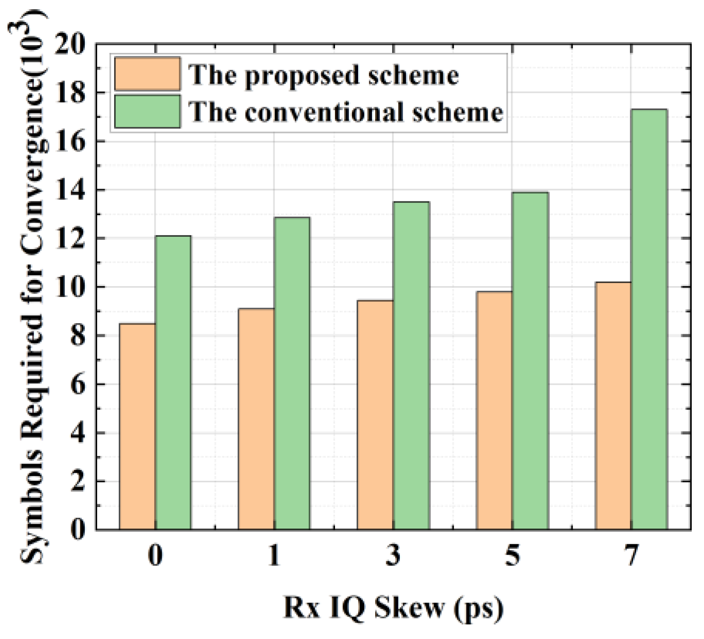
As shown in
Figure 11, the convergence costs required for establishing a timing synchronization loop using the proposed scheme and the conventional BFD scheme under different IQ skews at the receiver end are compared. The specific experimental conditions are SCO of 200 ppm, transmission 240 km SSMF, and amplitude imbalance and phase imbalance of 2 dB and 20 deg, respectively. When Rx IQ skew is in the range of 5 ps, the convergence cost of the proposed scheme is at least 33% lower than that of the conventional BFD scheme. When the Rx IQ skew is 7 ps, the proposed scheme reduces the convergence cost by about 56% compared with the conventional BFD scheme. The main reason is that the effect of ASE noise is introduced in the offline experiment, which leads to an increase in convergence cost in the conventional BFD scheme to establish a timing synchronization loop.
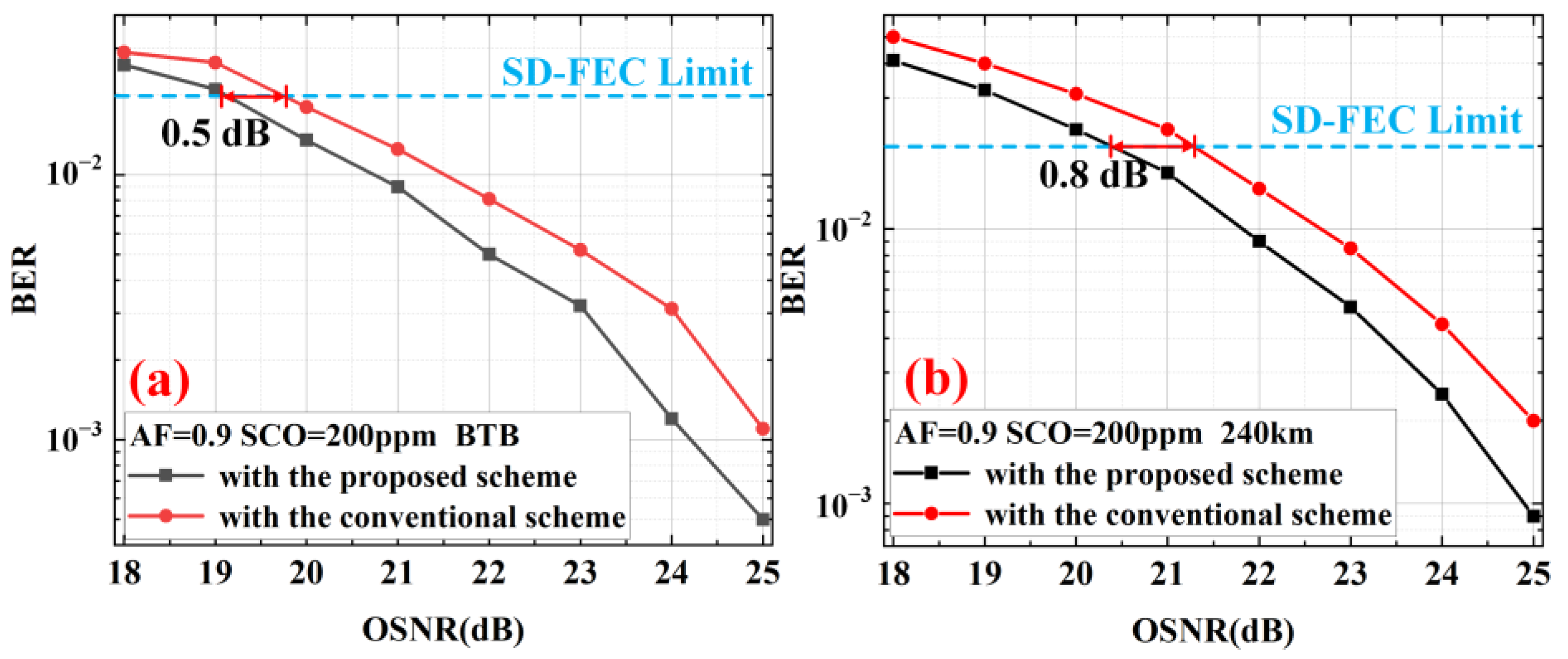
As can be seen from the three-carrier 40 GBaud PM-16QAM FTN system experimental results in
Figure 12, under the conditions of 0.9 AF and BTB transmission, the proposed scheme has about 0.5 dB OSNR tolerance improvement (@40 GBaud FTN PM-16QAM BER = 2 × 10
−2) compared with the conventional BFD scheme. Under the conditions of 0.9 AF and transmission 240 km SSMF, the proposed scheme has about a 0.8 dB OSNR tolerance (@40 GBaud FTN PM-16QAM BER = 2 × 10
−2) improvement compared with the conventional BFD scheme. The main reasons for the significant performance improvement of the proposed scheme over the traditional one are as follows. First, the proposed scheme uses the DDLMS algorithm for initial ISI equalization, thereby reducing the impact of severe ISI damage caused by aggressive FTN filtering on Rx IQ imbalance compensation. Second, the proposed scheme embeds a two-level Rx IQ imbalance compensation algorithm in the timing recovery feedback loop, further balancing ISI, sample clock offset, and part of the IQ imbalance damage in the FTN signal.
6. Conclusions
In this paper, a joint Rx IQ imbalance compensation and timing recovery scheme has been proposed and demonstrated, which could achieve a wider Rx IQ imbalance compensation range and reduce the convergence cost of timing recovery in high-symbol-rate and high-SE PM-16QAM FTN systems. The simulation results of 128 GBaud PM-16QAM FTN-WDM systems have demonstrated that the proposed scheme achieves compensation ranges of [−8, 8] dB for Rx IQ amplitude imbalance, [−45, 45] deg for Rx phase imbalance, and [−7, 7] ps for Rx IQ skew under a Q factor penalty of 0.1 dB. Compared to the conventional BFD scheme, the proposed scheme achieves improvements of 14% in Rx IQ amplitude imbalance, 12.5% in phase imbalance, and 16.6% in IQ skew compensation ranges. Furthermore, the convergence cost of timing recovery could be reduced by at least 31% under 0.9 AF. Meanwhile, the experimental results of three-carrier 40 GBaud PM-16QAM 0.9 AF show that the proposed scheme exhibits an OSNR tolerance gain of 0.5/0.8 dB compared with the conventional BFD scheme under BTB and 240 km SSMF transmission, respectively. In conclusion, the proposed scheme has the potential to realize efficient Rx IQ imbalance compensation and timing recovery in the practical application of FTN systems.

