Abstract
A review of the recent research work on high-power and high-speed (HPHS) Ge-on-Si photodiode design is presented, using Silicon Photonics (SiPh) technology, suitable for Radio-over-Fiber base station schemes. The Photodiode (PD) principle of operation, its structure for high RF photogenerated power, and the achieved PD wide bandwidth are presented. Then, the PD equivalent circuit models are introduced to obtain the PD S-parameters and operating bandwidth, such that efficient power coupling to mmWave loads is realized. Then, the PD theoretical transit-time and RC-time bandwidths are presented, and the PD photocurrent behavior against input optical power, and the optical signal manipulation techniques to improve the PD performance are also presented. After that, the impedance matching techniques between the PD output impedance and antenna input impedance are presented. Finally, recent photonic mmWave antenna designs are introduced.
1. Introduction
Global mobile traffic and the number of subscribers to the wireless network are increasing dramatically with time [1]. Therefore, the 5G network is the key solution for the wireless network to provide reliable connections for the incoming huge number of subscribers and applications. The communication data rates are increasing sharply [1]. Thus, fast optical components are replacing the slow electrical counterparts in communications systems so that data rates can be sharply increased. Thus, communications systems are developed into new schemes, as shown in Figure 1, where electric radio frequency (RF) components are directly interfaced with optical components [2]. Figure 2 shows that the optical-to-electric domain conversion can be achieved using high-power and high-speed (HPHS) photodiodes. It also shows that the conversion from the electric-to-optical domain is obtained by modulating optical sources. Furthermore, these photodiodes and optical modulators are connected to microwave components such as antennas or electric amplifiers [2]. The photodiodes for wireless communication applications must operate at high speeds for higher communication data rates and high RF photogenerated powers for enhanced Signal-to-Noise Ratios (SNRs) and signal coverage range.
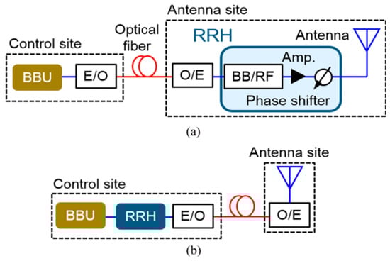
Figure 1.
Schematic illustration of the access network architecture. (a) Conventional digital baseband scheme. (b) Radio-over-Fiber-based scheme [2].
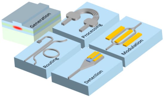
Figure 2.
Photonic integrated circuits include photonic light generation, photonic signal processing, photonic signal routing, optical light detection, and optical modulation [3].
Microwave photonics circuits are much easier to fabricate using the SiPh platform. On the other hand, if the photodiode is to be designed using the III–V semiconductor material, fabricating it is a complex and high-cost task. Thus, it leads to a complicated integration process with SiPh or CMOS systems. The Silicon Photonics technology applies the CMOS processing techniques to obtain photonic, optoelectronic, electronic, and microwave photonics circuits [3]. On a SiPh chip, various optical and electrical components can be installed and interfaced, such as Light-Emitting-Diodes, optical waveguides, optical signal processing components, photodiodes, optical modulators, antennas, mmWave circuits and so on [3]. Therefore, the SiPh platform provides an important opportunity for the optical and microwave components to be integrated on the same substrate, improving the data rates for the 5G technology and beyond.
The HPHS photodiodes can be designed using the III–V semiconductor material or achieved using Germanium-on-Silicon (Ge-on-Si) photodiodes of the Silicon Photonics (SiPh) technology. The III–V photodiodes (PDs) are sufficiently mature in realizing PDs (compared to Ge-on-Si PDs) with higher responsivity, lower dark currents, larger optical absorption due to their direct bandgap feature, bandgap engineering capability due to the available different lattice-matched compounds, higher operation speeds due to high carrier drift velocities and the ability to attain velocity overshoot, higher linearity, and higher RF photogenerated powers [4,5,6,7,8,9,10]. These III–V-based Modified Uni-Traveling Carrier (MUTC) PDs have been reported to provide 25 dBm at 30 GHz and 15 dBm at 60 GHz [10]. Hence, these III–V MUTC PDs have been reported to attain high output RF powers with wide operating bandwidths. However, the III–V photodiodes are currently incompatible with the existing procedures in SiPh foundries because many elements used for III–V materials are standard dopants for Complementary Metal-Oxide Semiconductor (CMOS) microelectronics. Therefore, processing tools and related drainage and exhaust systems are essential to avoid cross-contamination [11,12]. In addition, the CMOS microelectronics will be required to implement important changes in their processing and product/process development kit (PDK) such that the SiPh technology is capable of obtaining heterogeneously integrated III–V-on-Si PDs [12]. Moreover, when the III–V PDs are heterogeneously integrated into Si, many challenges must be overcome. In addition to the previously stated challenges, the important features of the III–V PDs are going to degrade when they are heterogeneously integrated on Si. Also, the large lattice mismatch and different thermal expansion constants between III–V materials and Si cause large strain and high misfit dislocation densities. As a result, the layers’ optical quality and PD performance (e.g., the PD dark current and sensitivity) are degraded [6,13]. Furthermore, the surface roughness and cleanliness requirements are applied for optimized heterogeneously integrated III–V-on-Si PDs. Moreover, buffer layers with good thermal conductivity between the Si wafer and a III–V PD will be essentially employed [11,14]. These buffer layers reduce the lattice mismatch between III–V materials and Si. However, they impose a challenge on the optical coupling efficiency from the Si waveguides to III–V PDs. As a result, the PD efficiency and bandwidths of these heterogeneously integrated III–V PDs are sharply decreased [8]. The heterogeneously integrated III–V PDs’ bandwidths are also going to decrease if the buffer layers are thick [8]. Lastly, heterogeneous III–V-on-Si PDs are produced with high costs and small throughputs [6]. Therefore, III–V PDs are very complex to be integrated with the Complementary Metal-Oxide Semiconductor (CMOS) technology, making them difficult to integrate with electronics. On the other hand, the Germanium-on-Silicon (Ge-on-Si) photodiodes are compatible with CMOS technology. They can be obtained with large-scale monolithic integration circuits, in addition to their low costs and low power consumption [15]. Hence, the Ge-on-Si PDs implemented using the SiPh technology are easily integrated with CMOS technology. Even though Ge has an indirect bandgap with a relatively small absorption coefficient, and weak optical absorption beyond 1600 nm and provides large dark currents when grown on Si as a PD because of existing crystal defects and a large thermionic emission coefficient [6,8,9], the Ge-on-Si PDs present a great potential for high-power and high-speed microwave photonic monolithic integrated applications because of their great compatibility with CMOS technology and low cost [2]. However, the reported Ge-on-Si photodiodes did not achieve as high powers as the RF powers achieved by III–V photodiodes, and they also did not achieve as wide bandwidths as the bandwidths achieved by III–V photodiodes. It can be seen from Table 1, which compares the HPHS III–V PDs [16,17,18,19] (implemented on a native Indium Phosphide (InP) substrate) performance with the performance of HPHS SiPh Ge-on-Si PDs, that the Ge-on-Si PDs compete with the III–V PDs at low-frequency operations in terms of RF photogenerated power, responsivity, and dark current. However, the III–V PDs sharply surpass the Ge-on-Si PDs at high-frequency operations [20,21]. Therefore, the motivation for this review article is that the design of HPHS SiPh Ge-on-Si PDs should be adopted instead of the III–V PDs because Ge-on-Si PDs are compatible with CMOS technology, low cost, and they could compete with III–V PDs performance if carefully developed [22,23,24,25,26,27,28].

Table 1.
Comparison table between SiPh Ge-on-Si PDs and III–V PDs grown on a native InP substrate.
However, the wafer bonding technologies have been developed in recent years to integrate the III–V photodiodes onto Silicon platforms. Different integration techniques, including direct wafer bonding [29], plasma-activated direct bonding [30], adhesive bonding [11], flip-chip integration [11], hetero-epitaxial growth [11], metal-assisted bonding [31], poly-Si bonding and multigrading bonding layer techniques [32], are employed to integrate III–V PDs onto Si circuits. However, there are many challenges facing these wafer bonding technologies. Direct wafer bonding, including micro-transfer printing [29], requires several prerequisites, such as low surface roughness on both materials to avoid weakening the bonding strength and a clean bonding environment. Also, the different thermal expansion coefficients between the two materials would weaken the bonding contact under mechanical forces or thermal dynamics. Furthermore, the reliability and durability of direct-bonding devices are another challenge, in addition to the development of reliable characterization and testing methodologies. Additionally, the different work functions between materials in the direct-bonding devices influence the barrier height at the interface between the conduction bands of the two materials. Therefore, a Schottky barrier at the interface between the two materials is introduced, reducing the carrier transmission across the interface and the device efficiency. The direct-bonding devices should also be optimized to reduce the required reverse bias, and the ON resistance, and to increase the linearity of the PD. These devices should also undergo different treatments to operate with passivated surface states, reduced interface defect density, and a heterojunction of quasi-ohmic characteristics. The direct-bonding technology can obtain PDs with good responsivities at important communication bands, and they are highly reproducible, allowing for larger-scale production of these heterogeneous PDs. However, many other challenges must be overcome, especially for micro-transfer printing, such as accurate control of the undercut etching processes, uniformity control across large wafer surfaces, and printing optimization using large, arrayed stamps. On the other hand, plasma-activated direct bonding can achieve stronger bonding between wafers and does not require very high process conditions. O2 or N2 plasma activation can be used to achieve the bonding between III–V PDs and Si wafers. The surface should be cleaned of contaminated particles and organic matter in this bonding technology. Additionally, the III–V and Si wafers require cleaning. After that, the wafer surfaces are bombarded with O2 or N2 plasma, causing changes to the surface composition of III–V and Si wafers. The surface roughness and defect state are effectively suppressed during the process of the plasma-activated direct bonding technology. Additionally, the equivalent stress for bonding and deformation should be analyzed to ensure strong bonding. The bonding interface performance should also be examined after applying the plasma to ensure strong bonding. Another integration technology is the flip-chip bonding process, which requires accurate alignment during assembly, and hetero-epitaxial growth, where it is challenging to grow high-quality III–V materials on Silicon. On the other hand, using adhesive bonding (instead of molecular or anodic bonding) provides important advantages, as the adhesive bonding process obtains planarized surfaces, and the surface cleanliness and surface roughness requirements are relaxed. As a result, the bonding preparation process is sharply reduced. The adhesive used for bonding is the DVS-BCB (divinylsiloxane-bis-benzocyclobutene). DVS-BCB adhesive provides important advantages, including a low curing temperature, high optical clarity, a high degree of planarization, good thermal stability, good chemical stability, low moisture absorption, and wide applicability. However, the disadvantage of the DVS-BCB is its low thermal conductivity, which requires that the adhesive be used with thin thicknesses, especially for high-power devices. Many other challenges are facing adhesive bonding technology. The chemical mechanical polishing process is required to planarize the surface. Additionally, achieving efficient optical coupling from the Silicon waveguide to the III–V device layer is a critical task. This efficient optical coupling should operate within the required optical wavelength range and be fabrication-tolerant. Therefore, an adiabatic taper scheme is developed for the waveguide-integrated III–V devices, and a diffractive grating structure is used for bonded surface-illuminated III–V devices. Another crucial wafer bonding technology is metal-assisted bonding [31], where copper-to-copper hybridization bonding is employed to connect III–V PDs onto a Silicon integrated circuit, and high sensitivity and low dark current are obtained in the wavelength range from visible to short-wavelength infrared. The bonding methodology in [31] combines the die-to-wafer process and copper-copper hybridization. The challenges facing this metal-assisted bonding technology are to obtain a finer pitch size between the PD elements in an array to provide higher productivity, scalability, and yield. Additionally, the flatness of the III–V/Si heterogeneous wafer and the bonding process conditions should be optimized with consideration of the different thermal expansion coefficients of the materials. Furthermore, the Cu-Cu bonding interface of the III–V PDs to the Silicon circuit should be obtained without defects. Also, thinning processes should be applied to the InP layer to enhance the PD sensitivity. Another available challenge is that wafer dicing, InP thinning, and bonding of different materials cause crystal defects and distortion, which increase the PD dark current. Therefore, the die-to-wafer and Cu-Cu bonding processes should be optimized to avoid process damage. In addition, when the pitch size between PD elements is reduced, the dark current is expected to increase due to the relatively larger p/n junction area, and the PD is more susceptible to surface defects because of the use of an ultrathin n-InP layer. Another challenge is that the process margin should also be wide, and good repeatability is obtained for the employed bonding technology. Poly-Si bonding and multigrading bonding layer techniques [32] could also be used to achieve a heterogeneous III–V PD on Si. When epitaxial growth technology and heterogeneous bonding technology are employed to prepare III–V materials on Si, the main challenge facing these technologies is to overcome the high threading dislocation density caused by the lattice mismatch between Si and III–V materials. Also, polycrystalline and amorphous bonding are applied to eliminate gas bubbles at the bonded interface. However, the conduction band offset at the InGaAs/Si interface is high, making it difficult for electrons to cross this band offset, which degrades the frequency response because the transit time increases. Therefore, multigrading layers are used to decrease the lattice mismatch and conduction band offset. Additionally, high performance heterogeneous devices with optimized dark currents are obtained when bonding layers with different band gap energies and band tails are employed. The number of multigrading layers should be optimized to reduce the PD dark current, and reduce the conduction band offset. Additionally, the electric field in the heterogeneous PD is engineered using multigrading layers and bonding layers to enhance the PD performance. The bonding layer band gap should also be optimized to increase the PD photocurrent, improve the PD linearity, and enhance the PD bandwidth. Finally, these heterogeneous bonding methods still involve materials and process steps, such as the use of InP, GaAs, and III–V etch chemistries, that are generally not compatible with standard CMOS processing lines. In contrast, Ge-on-Si photodetectors benefit from the ability to monolithically grow Ge layers directly on Si, which is more readily integrated within CMOS foundries and avoids bonding-related interface issues and potential contact leakage. Thus, while wafer bonding of III–V materials enables superior performance in some applications, it remains a non-CMOS-compatible process in strict terms.
This review article presents the recent developments in high-power and high-speed photodiodes used for Radio-over-Fiber (RoF) 5G wireless technology at the 5G mmWave FR2 frequency band. This article is organized as follows: Section 2 summarizes a recent review study for HPHS Ge-on-Si photodiodes, Section 3 presents important applications for microwave photonics circuits using HPHS photodiodes, Section 4 presents future directions and applications for HPHS Ge-on-Si RF PD design, and Section 5 concludes the paper.
2. High-Power and High-Speed RF Photodiodes
It has been reported that the photodiodes designed based on the III–V semiconductor material on an Indium Phosphide (InP) substrate can provide high output RF powers that can sufficiently cover the required wireless ranges for 5G base-station radiations at mmWave frequencies [10]. The RF photogenerated power of III–V photodiodes reaches 25 dBm at 25 GHz and 15 dBm at 65 GHz [10]. However, the III–V photodiodes are complex and high-cost to fabricate, and they are challenging to integrate with CMOS and SiPh technology. On the other hand, the Ge-on-Si photodiodes, designed using SiPh technology, could provide sufficient output RF photogenerated powers at mmWave frequencies. Many high-power and high-speed (HPHS) Ge-on-Si photodiodes have been recently reported to be implemented for microwave photonics applications [5,6,7,8,9,10,11,12,13,14,15,20,22,23,24,25,26]. HPHS Ge-on-Si photodiodes can be achieved when the Ge absorbing region is optically fed using evanescent coupling with double lateral Silicon Nitride waveguides [33], or when the light is laterally incident on the PD using evanescent coupling [34]. They can also be obtained using a mode-evolution-based (adiabatic) coupler, illuminating the light into the Ge region uniformly to reduce the saturation effects at high input optical powers [35,36]. Also, the PD power and speed could be enhanced when the PD is vertically incident with light and when Metasurface arrays are used to enhance the optical light intensity in the PD absorption region [37,38,39]. In addition, they can be achieved when many photodiodes are connected in parallel to form a photodiode linear array [40,41,42,43,44,45,46]. Also, when the photodiode doping concentrations are regulated, the space-charge screening effects sharply decrease [47]. In addition, HPHS photodiodes (PDs) can be achieved when the PD is constructed using stacking N-, intrinsic- and P-type doped regions, and the light is evanescently coupled into the Ge region [48,49]. Furthermore, HPHS PDs can be obtained using the Uni-Traveling Carrier (UTC) approach, where the electrons are the only allowed carriers, and the slow holes are blocked and excluded [15,50,51,52,53,54,55]. UTC PDs can also be obtained using the III–V materials, which are then integrated heterogeneously on the Silicon (Si) substrate [56]. The Avalanche gain can also provide HPHS Ge-on-Si PDs [57,58,59,60,61]. However, most Avalanche PDs are designed for data communications applications at the O-band for short-distance communications. Traveling-wave photodiodes can also achieve HPHS PDs [62,63,64,65]. It was also found that when the optical field is manipulated properly around the Ge absorbing region, higher output RF powers are expected to be obtained from the PDs [66]. Furthermore, using Si/Ge waveguide phototransistors could enhance the responsivity sharply, as proposed in [67]. Table 2 presents the performance comparison between the introduced HPHS Ge-on-Si PDs.
Table 2.
Comparison table between the introduced HPHS Ge-on-Si photodiodes in this article.
It is worth mentioning that Germanium is a good medium for absorbing optical signals with wavelengths slightly shorter than 1600 nm [70]. The absorption coefficients of the Ge medium are at , and at . Therefore, the Ge material is a perfect option to be used as the absorbing medium for photodiodes used for data centers at 1300 nm, and it is also a good option for the photodiodes that can be used for 5G RoF base stations at 1550 nm. However, InGaAs material is more efficient at 1550 nm wavelength; but, Ge is used for PD design as it is much easier to integrate within a Silicon chip using the SiPh platform. Figure 3a presents the band diagram for Ge after applying biaxial tensile strain to make Ge behave as a direct bandgap semiconductor, where the bandgap energy between the valence band and the Г conduction band is 0.53 eV. The indirect bandgap energy for Si is 1.12 eV, which is much higher than the bandgap energy of Ge. Figure 3b presents the band diagram (when the PD is at reverse bias) and the PD structure for the Ge-on-Si PD proposed in [50], where the carrier transport principle is shown. It can also be seen from Figure 3b that the bandgap energy for Ge is smaller than that of Si. Therefore, the introduced dark current in the Ge region is more than the dark current contributed by the Si region. In addition, the Ge-on-Si PDs provide higher dark currents compared to III–V PDs because of the available crystal defects due to lattice mismatch between Ge and Si, the smaller Ge bandgap energy, poor passivation and higher trap densities at the Ge/Si interface, higher Ge surface recombination velocity, and the large thermionic emission coefficient [6]. On the other hand, the III–V PDs have lower dark currents because the III–V materials are lattice-matched with lower defect densities, have higher bandgap energies, and are grown with better-controlled epitaxy and high-quality heterojunctions with fewer interface traps.
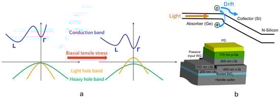
Figure 3.
(a) Band diagram for the Ge at equilibrium after applying biaxial tensile strain [49], and (b) the Ge-on-Si PD band diagram when it is reverse biased at 5 V [50].
2.1. Photodiode Principle of Operation and PD Structure Design
When the light is evanescently coupled from double lateral waveguides to the Ge region, the PD is expected to provide high-power and high-speed operation [33,71]. The evanescently coupled PD is shown in Figure 4. The light distribution in the absorption Ge region is uniform due to the tapering of the lateral waveguides. As a result, the photogenerated carriers are not concentrated at a specific location, and the operating bandwidth of the PD is increased. In addition, the applied electrostatic field between the PD electrodes is also sufficiently strong due to the doping concentrations used for the N+-, P-, and P+-region. Therefore, the collection of the photogenerated carriers is fast and efficient. The lateral waveguides are sufficiently long, so the injected photons are fully absorbed as they travel along the Ge region. Phase matching between the waveguide and Ge region modes should be attained to obtain efficient light coupling [72]. Many parameters affect the mode coupling condition, such as the waveguide thickness, the Ge region thickness, the refractive indices of the waveguide and Ge region, and the operating wavelength.
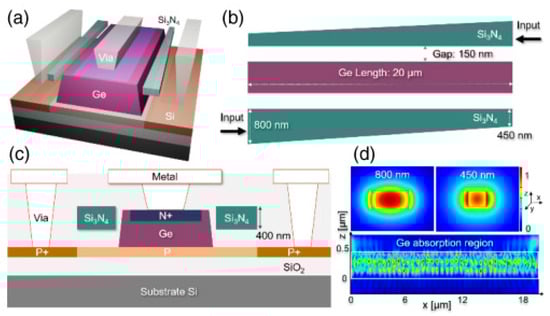
Figure 4.
The Ge-on-Si photodiode using double lateral optical waveguides [33]. (a) Side view of the photodiode, (b) top view of the PD, (c) cross-sectional view of the PD, and (d) electric field distribution across the waveguide and along the Ge absorbing medium.
When the photodiode is operated under high-power conditions, that is, when the input optical power is 10 mW or more, then the photodiode suffers from degraded linearity, heat failure occurrence, losing the mode matching between the waveguide and Ge region, and accumulation of charges causing the space-charge effects to take place. The mode-evolution-coupling technique can achieve HPHS PDs [35,36]. Figure 5 shows the proposed mode-evolution-based coupled HPHS PD in [36]. The optical light is divided into two optical waveguides using a Multimode Interferometer (MMI) power divider such that two parallel Ge regions are equally fed using the mode-evolution-based coupling technique. The mode-evolution-based coupler comprises the waveguide bend and the linearly tapered waveguides. The waveguide bend reduces the mode mismatch between the waveguide and the Ge region. Therefore, the bend radius should be as large as possible to achieve a gradual mode transition. The waveguide taper allows the light to couple into the Ge region gradually and efficiently; as a result, a uniformly distributed optical generation rate along the PD length is obtained, and the PD saturation current is improved. The waveguide taper length should be as long as possible to increase the PD responsivity; however, the PD bandwidth will be reduced due to increased capacitance. It is worth noting that when the Ge region was divided into two halves, the input optical power at each Ge region was reduced by half, the space-charge effects were much reduced, and the saturation current was much improved. The proposed HPHS PD in [36] has a dark current of 73 nA at reverse bias and a photocurrent of 9.4 mA at an input optical power of 20 mW. The high-power operating bandwidth of the PD is 31.6 GHz when the input optical power is 4 mW.
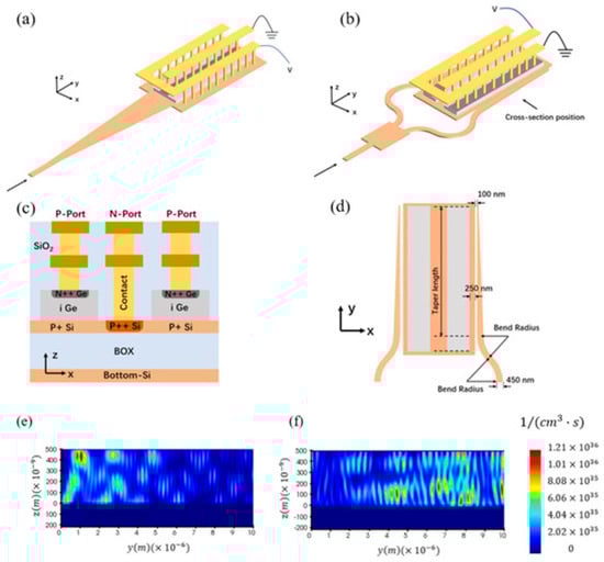
Figure 5.
(a) Butt-coupled PD with long taper. (b) Proposed mode-evolution-based coupled PD [36]. (c) Cross-section view of the proposed PD. (d) Top view of the proposed PD. (e) Optical generation rate for the butt-coupled PD. (f) Optical generation rate for the proposed mode-evolution-based coupled PD.
Furthermore, the Ge regions can be connected in parallel using a single Ground-Signal-Ground (GSG) terminal to enhance the output power of the photodiode [40,41,42,43,44,45,46,68]. When two Ge regions are connected in parallel, the total Ge area is increased twice. As a result, the junction capacitance increases by a factor of two, and the series resistance decreases by a factor of two also; as a result, the PD RC-time bandwidth is not changed, and the PD saturation current is sharply increased. Hence, the PD output RF power is increased sharply as well. The array of two elements proposed in [40] is illuminated by light from the front and back sides of the Ge regions; as a result, the absorption rate along the Ge regions has a uniform distribution, causing the space-charge effects to be reduced sharply, and at the same time, the saturation current increases sharply. In addition, when the PD is illuminated by light from both (front and back) sides, the applied optical power on the Ge regions is reduced by a factor of 0.5, which sharply decreases the chances of thermal failures. The dark current of the PD array has increased compared to the dark current of the single-element PD.
When the number of elements of the PD array is increased to more than two elements, the PD array saturation current will be increased. Still, the PD array RC bandwidth will be changed from that of the single-element PD because the PDs’ resistances will not be connected in parallel. Therefore, the RC bandwidth of the PD array can be calculated using the transmission matrix method to analyze the resulting complicated PD equivalent circuit, as was proposed in [41], where all the Ge regions share the same P+ doped region. It was found that when more than two array elements are used, the PD array bandwidth will be reduced as the increase in junction capacitance will be the dominant affecting factor, and the array total resistance will not decrease. However, the bandwidth of the PD array can be enhanced using inductive peaking techniques and transmission line theory. The saturation current of the PD array with more than two array elements will gradually increase because there will be high power losses in the P+ doped region resistances and due to out-of-phase currents flowing in these resistances [41].
Traveling wave PD array (TWPD Array) can also be designed to avoid bandwidth reduction when more than two PD elements are used in the array [42,69]. The used single-element PD for the four-element TWPD Array proposed in [42] is a PIN PD [48,72,73,74] with a high photocurrent and a wide bandwidth. The impedance matching between the TWPD Array and a 50 Ohm load is accomplished by optimizing the GSG coplanar-waveguide electrodes connected to the four PD elements, considering the periodic capacitive PD loading. In addition, Figure 6 shows the proposed TWPD Array in [42], where optical delay lines match the optical velocity with the electrical velocity. On the other hand, Figure 7 shows the proposed TWPD Array in [43], which has single-element PDs illuminated from the front and back sides, thereby doubling the power handling capability of the PD array.
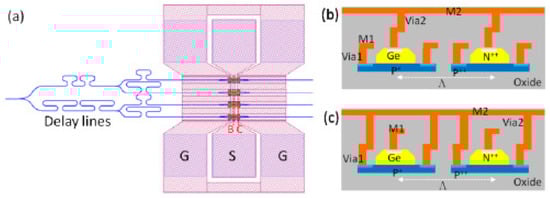
Figure 6.
(a) Traveling wave PD array in [42], (b) signal metal connections to the single-element PDs at the B position, and (c) ground metal connections to the single-element PDs at the C position.
Figure 7.
The high-power and high-speed dual-illuminated TWPD Array in [43].
The traveling wave photodiode approach was also used to provide a high-power and high-speed photodiode as proposed in [62,63]. The traveling wave photodiodes are designed with metallic electrodes that achieve impedance matching with an external circuit. The transmission line theory matches the impedance between the microstrip or coplanar waveguide electrode lines of the PD and the output circuit (50 Ohm load, for example). The input terminal of the electrodes will also be connected to a matched load such that the backward traveling waves are absorbed and not reflected in the transmission lines. Hence, the TWPD bandwidth is engineered using the transmission line theory. The PD RC-time bandwidth, carrier drift time, carrier diffusion, carrier trapping, and the bandwidth of velocity matching between the electrical and optical signal will also impact the overall PD bandwidth. It can be seen from Figure 8 that the proposed TWPD in [63] is optically dual-injected and evanescently coupled to the Ge region. The TWPD length is optimized to achieve the best PD performance when the uniform light distribution occurs in the Ge region because the left- and right-incoming optical signals will add up constructively to provide a uniform distribution. As a result, the effective absorption area is increased, and the saturation performance is much improved. The RC time constant, the carrier transit time, and the electrode length limit the 3 dB bandwidth of this proposed TWPD. When the PD electrodes are longer, the PD capacitance and transmission line loss are increased; as a result, the PD bandwidth decreases. Also, when the PD length provides a non-uniform light field distribution, the bandwidth will decrease because of increased space-charge screening effects. Also, the PD bandwidth decreases when the input optical power increases due to the increase in the space-charge effects and the much higher probability of carriers’ collisions with the lattice.
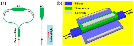
Figure 8.
(a) Incident light is split into two beams to feed the PD, and (b) the proposed dual-injection PD in [63].
The HPHS PD can also be realized when doping concentrations are regulated to reduce space-charge effects significantly [47]. The doping-regulated Ge-on-Si PD is shown in Figure 9, where it can be seen that the Ge region is sandwiched between the N++ doped region and the P+ and P++ doped regions. When the doping concentration in the P+ collection layer is increased, the number of holes in the collection layer is much higher than the photogenerated carriers in the absorption Ge region, and the built-in electric field is much enhanced. As a result, the carriers’ transport speed is much enhanced such that it achieves saturation velocity, the carriers’ transit time is much reduced, the probability of carriers recombination is reduced, the photocurrent and saturation current are much increased, and the space-charge effects are eliminated.
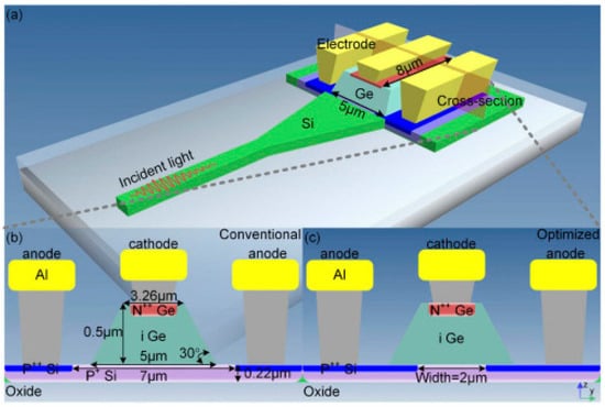
Figure 9.
(a) 3D view of the doping-regulated PD in [47] and (b) PD with conventional doping regions. (c) The PD with the optimized doping regions.
In addition, when the optical signal is coupled evanescently to the Ge region of the PIN PD, then High-Power for High-Speed PDs can be attained, as was reported in [48,49]. Also, Uni-Traveling Carrier (UTC) PD, where the only allowed carriers are the electrons, can be designed based on the Ge-on-Si approach (as shown in Figure 10) [15,50,51,52,53,54,55], or using the heterogeneously integrated III–V material on Silicon (Si) to achieve HPHS PD performance [56]. The SiPh UTC Ge-on-Si PD design is different than the design of III–V UTC PDs because it is a complex task to engineer the bandgap for the Ge-on-Si PDs; i.e., it is difficult to grow a diffusion-blocking layer for the Ge-on-Si PDs. However, UTC Ge-on-Si PDs are designed such that the capacitance per unit area is decreased to improve the PD bandwidth, and a higher breakdown voltage is achieved to obtain higher power performance. Therefore, the Ge region is entirely p-doped, while the intrinsic region and n-doped region are attained in the Si, as shown in Figure 10a. As a result, the PD capacitance and breakdown voltage are controlled by the Si collector thickness instead of the Ge absorber thickness. The Ge absorber thickness, on the other hand, controls the PD quantum efficiency by improving the absorption profile and length and enhancing the collection efficiency. The absorption profile is improved when the optical coupling from the passive waveguide to the absorption region is maximized by optimizing the absorber thickness, and the collection efficiency is improved when the back-surface recombination velocity is decreased. The Ge absorber region is p-doped with a graded doping profile from at the metal contact side to at the Ge/Si interface side, so that an electric field is induced in the Ge absorber to improve the PD bandwidth and efficiency. The strength of this induced electric field is inversely proportional to the Ge thickness. Therefore, the collection efficiency is enhanced when the Ge thickness is reduced. The collection efficiency is controlled using the induced electric field strength, the surface recombination velocity, and the electrons’ exit velocity to enter the collector. The 3 dB bandwidth of the UTC PD is enhanced when the absorber thickness is also decreased because of the enhanced induced electric field in the absorber. An optimum value for the Ge absorber thickness that would obtain the optimal PD quantum efficiency and bandwidth must be implemented. This optimal Ge thickness can be obtained using the drift-diffusion equations for a one-dimensional photodiode using the same approach in [75].
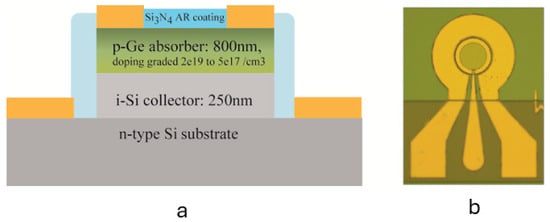
Figure 10.
(a) Cross-section view for the Ge-on-Si UTC PD in [52]. (b) Photo of the fabricated PD.
Finally, the Avalanche gain can increase the Ge-on-Si PD output power as proposed in [57,58,59,60,61]. However, these Avalanche Ge-on-Si PDs are reported to be used for data (short distance) communications within data centers and not for 5G base stations with the RoF scheme. Hence, they are briefly presented here to show that using the Avalanche gain could introduce the opportunity of achieving HPHS PDs for 5G base station applications. The proposed Avalanche Photodiode (APD) is presented in Figure 11, which shows an example of an APD design. The proposed APD design achieves a bandwidth of 18.9 GHz, a DC photocurrent gain of 15, and a sensitivity of −11.4 dBm at a reverse bias of −6 V. Figure 11 shows that the APD has three terminals. The Ge region is installed on top of the Si waveguide, and the waveguide is installed on top of a Si substrate. The optical signal is evanescently coupled to the Ge region for absorption. The top side of the Ge region is P-doped and connected to terminal one. At the same time, the Si substrate is composed of interdigitated N- and P-doped fingers spaced using intrinsic Silicon. The P-doped fingers are connected to terminal two, and the N-doped fingers are connected to the third terminal. As a result, two reversed-bias PIN diodes are realized, and the light absorption region is independently controlled from the charge multiplication region.
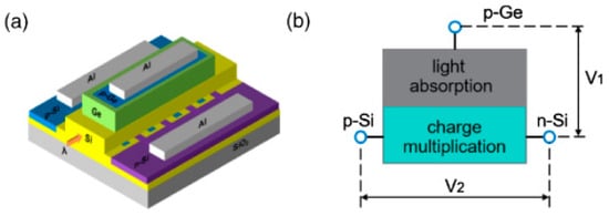
Figure 11.
(a) The APD design in [60] and (b) absorption and charge multiplication region.
It can be noted from Table 2 that the dark currents for the 4-element TWPD array [43], 8-element PD array [44], PIN PD [48] and Si-based UTC PD [50] are very high. The PD array has high dark currents in [43,44] because the dark currents from the employed single-element Ge-on-Si PDs are added. The evanescently coupled PIN PD in [48] suffers from high dark current because the thermal conductivity of the PD materials decreases as the junction temperature increases. The heat is generated because of high photocurrent, and consequently, the dark current is increased. The Si-based UTC PD [50] suffers from high dark current due to the dielectric layer’s breakdown on the device’s sidewall. On the other hand, the SNRs for the Ge-on-Si PDs presented in Table 2 were calculated using Equations (9)–(17), shown later in the paper. The presented SNR values in Table 2 were not taken from the mentioned references. However, the SNR values in Table 2 are calculated using Equations (9)–(17), while the other parameters in Table 2 were obtained from the mentioned references. It can be seen from Table 2 that the array PDs achieve the highest SNR with a value of 73.7 dB [69], followed by the evanescently coupled PD [48] with a second-highest SNR at 66.47 dB, and then the UTC PD [15,55] achieved a comparable SNR at 64.02 dB. The adiabatic-coupled PD [36] obtained a lower SNR value of 56.64 dB. The doping-regulated PD [47] obtained a comparable SNR value of 54.52 dB. The Traveling Wave PD also provided a comparable SNR value of 53.52 dB. These attained SNRs for the HPHS Ge-on-Si PDs are reasonable because the dark currents for these high-power PDs have a negligible impact on the SNR value. Conversely, the photocurrent value and the operating bandwidth are the primary parameters affecting the PD SNR value. Therefore, the PD arrays, especially when the TWPD is used as the single element, the evanescently coupled PDs, UTC PDs, and adiabatic-coupled PDs, are expected to obtain the highest SNR values due to the attained high RF photogenerated powers at high PD speeds.
The PD can be considered a high-power PD when the input optical power is around 10 mW (10 dBm) [36]. High-power PDs suffer from thermal effects, degrading the PD linearity and causing PD failure, mode mismatch, and high space-charge effects. The PD could be optically fed using a normal incidence or an edge incidence with a waveguide integration approach. A trade-off exists between PD quantum efficiency, bandwidth, and dark current when the normal-incidence PD is implemented. This trade-off can be overcome when the waveguide-type PD (with edge incidence approach) is employed because the light propagation (absorption) direction is perpendicular to the carrier collection direction [51]. Hence, the carrier collection path is decoupled from the light absorption length. As a result, high-speed waveguide-type PD can be accomplished with almost maximum quantum efficiency [51]. Phase matching between the waveguide and Ge region modes must be obtained for the waveguide-type PDs so that the optical light is efficiently coupled from the optical waveguide to the Ge absorption region. The efficiency of mode coupling from the waveguide to the Ge region is improved by optimizing the waveguide thickness, the Ge region thickness, and the refractive indices of the waveguide and Ge region. As was presented earlier, the HPHS Ge-on-Si PDs can be designed based on different approaches, including when the PD is evanescently coupled using double lateral optical waveguides, when the PD obtains uniform optical distribution utilizing the mode-evolution-based (adiabatic) coupler, when the single-element PDs are connected in parallel to form a PD array, when the PD doping concentrations are carefully regulated, UTC PD design, traveling wave PD design, or when Metasurface arrays are used with vertical (or normal) incident PDs. The evanescently coupled Ge-on-Si PDs [33,34,48,49,71,74], the mode-evolution-based (adiabatic) coupled Ge-on-Si PDs [35,36,68], the Ge-on-Si PDs with regulated doping concentrations [47,71], and the traveling wave Ge-on-Si PDs [62,63,64,69] accomplish high power and high-speed performance by sharply mitigating the space-charge effects. The Ge-on-Si PD arrays [40,41,42,43,44,45,46,68,69] improve the high-power performance by connecting many single-element PDs in parallel, while the array PD bandwidth is either not varied with two-element PD array, or degraded when more than two elements are connected. The UTC Ge-on-Si PDs [15,50,51,52,53,54,55] improve the high-power performance by increasing the breakdown voltage and improve the high-speed performance by decreasing the PD capacitance. This is obtained for the UTC PDs because the Si collector region controls the PD capacitance and breakdown voltage, while the Ge absorption region controls the PD quantum and collection efficiency. The vertical incident PDs with Metasurface arrays [37,38,39] obtain high power and high speed because the Metasurface structures enhance the optical light intensity in the absorption region sharply. Now, for the PD array design, the space-charge effects are not mitigated when single-element PDs are connected in parallel. However, the saturation current of the PD array is sharply increased because of the added saturation currents from each single-element PD. This higher saturation current for the PD array is attained at the cost of increased PD size, reduced scalability because of increased fabrication complexity, and bandwidth reduction if more than two elements form the PD array. Hence, the PD arrays presented in Table 2 provide the highest saturation currents with lower PD bandwidths. This bandwidth reduction disadvantage for the PD array design can be overcome using the traveling wave PD design approach ([43] in Table 2) because the PD bandwidth can be optimized using the transmission line theory, instead of being limited by the PD RC time bandwidth. On the other hand, Table 2 shows that the evanescently coupled PDs, adiabatically coupled PDs, and UTC PDs achieve the best PD bandwidths. The evanescently coupled PDs and adiabatically coupled PDs achieve the best bandwidths because uniform optical absorption is obtained in the Ge region to reduce the space-charge effects sharply, and a strong electric field is attained (due to the positive and negative doping concentrations) in the Ge region to decrease the carrier transit time. Also, the high saturation currents and responsivity for the evanescent and adiabatic coupled PDs are achieved because of orthogonal absorption and collection paths, and the capability of detection at higher optical powers. The saturation currents and responsivity for the evanescently coupled PDs can be further improved using a Distributed Bragg Reflector (DBR) so that the unabsorbed light is reflected back to the absorption region to be absorbed again [34]. However, the optical signal in this PD was incident on the longer side of the Ge region (it is a lateral incident PD), which is different than typical evanescent coupled PDs. The lateral evanescent incident PD in [34] achieves (compared with the other evanescently coupled PDs) higher and consistent coupling efficiency, minimal processing demands, and minimal effect from operating temperatures. The mode-evolution-based (adiabatic) coupled PDs [35,36,68] are more suitable for high-power microwave photonics applications than evanescent coupled PDs [33]. The evanescent coupled PDs’ bandwidth and responsivity would be degraded at high-power operations due to higher photogenerated-carrier-induced thermal effects and higher space-charge effects because of the strong and fast optical coupling occurrence. On the other hand, adiabatic coupled PDs provide gradual optical coupling between the waveguide and the Ge region. As a result, the optical field distribution in the Ge region is more uniform. This uniform optical absorption improvement of adiabatic coupling can also be seen in Table 2, where even though the adiabatically coupled PDs [36,68] are shorter than the evanescently coupled PD [33] by half of the length, the adiabatically coupled PDs have competing saturation currents and bandwidths. Also, the adiabatically coupled PDs (compared to evanescently coupled PDs) are more robust against dimensional tolerances and temperature variations. Silicon Nitride waveguides were also used for the evanescent coupled PD in [33] because of their lower nonlinearity, much lower propagation loss, and broader transparent window for light propagation than Si. Hence, the scalability of the evanescent coupled PD in [33] is degraded because some foundries do not provide the Silicon Nitride layer. In addition, the evanescently coupled PD in [33] and the adiabatically coupled PD in [36] employed doping at the Ge region, which also reduced their scalability, as the doping and contact of Ge may not be accessible in some foundries. However, the adiabatic coupled PD in [68] overcomes these limitations by obtaining an HPHS PD without Ge doping and Silicon Nitride integration. Furthermore, the saturation currents and bandwidths of evanescent and adiabatic coupled PDs are improved when the doping concentrations are carefully regulated [47,71] at the cost of increased fabrication complexity and degraded PD scalability. The UTC PDs can also attain high power and high-speed performance, as shown in Table 2, and their performance competes with the evanescently coupled and adiabatically coupled PDs. The waveguide-coupled UTC PDs provide higher bandwidth [50,54], while the normal incident UTC PDs provide higher saturation currents [15,52,53,55]. All the presented Ge-on-Si PDs in this section (except for the heterogeneously integrated III–V PD on Si [56]) are CMOS-compatible. The array PDs achieve the highest saturation currents but suffer from degraded bandwidths, which can be overcome using the traveling wave PD as the single-element PD [42,43,64,65,69]. The bandwidth of the TWPDs is limited by the RC time, carrier drift time, carrier diffusion, carrier trapping, and velocity-mismatch between electric and optical signals bandwidth. However, the TWPDs bandwidth is enhanced using the transmission line theory. Therefore, the TWPD bandwidth is improved when the transmission line connected to the PD is well optimized. The HPHS TWPD [63] can be achieved with a shorter PD length as long as uniform optical distribution occurs in the Ge absorption region. The HPHS TWPD in [18] has a length of 6 that is shorter than the lengths of evanescent and adiabatic coupled PDs. Hence, the scalability of the TWPDs is improved compared to the evanescent and adiabatic coupled PDs, in addition to their competing PD performance and easier fabrication. The dual injection strategy is utilized for the TWPD to obtain a uniform optical distribution in the absorption Ge region. As a result, wider bandwidth and higher output power are accomplished with a shorter PD length. The dual optical illumination is implemented to mitigate the space-charge effects and improve the PD power handling capability. The dual injection strategy was also used for the evanescent coupled PDs, adiabatic coupled PDs, and PD arrays.
The dominant sources of PD nonlinearity are the voltage- and current-dependent responsivity, voltage- and current-dependent PD capacitance, and the absorption and carrier-dependent carrier velocities related to a perturbed electric field because of space-charge and loading effects [76]. The linearity of the Ge-on-Si PDs is going to degrade with the increase in the PD RF photogenerated power or the PD operating bandwidth. The third-order Output Intercept Point (OIP3) degrades at higher power or higher speed operations, and it is improved when the bias voltage or the photocurrent is increased because of reduced space-charge effects. The evanescent coupled PD [33] and adiabatic coupled PDs [36,68] accomplish a good linearity performance until a photocurrent of 12 mA at an input optical power of 14 dBm and 17.7 mA at an input optical power of 13.42 dBm, respectively. The evanescent coupled PD in [48] was also capable of achieving high linearity performance until a high output power of 12 dBm at a photocurrent of 50 mA at 1 GHz (with an OIP3 of 36.49 dBm), and high linearity performance also at 25 GHz until an output RF power of −5 dBm at a photocurrent of 7 mA (with a 10 dBm input optical power) [34]. The PD linearity is improved when the Ge-on-Si PD has regulated doping concentrations [47], where the 1 dB compression photocurrent at 20 GHz was improved from 4 to 5.3 mA, enhancing the linear output RF power range. However, it is noted that the doping-regulated PD in [47] has a degraded PD linearity at higher operating frequencies and lower bias voltages. The Ge-on-Si UTC PDs also attain good linearity performance at lower operating frequencies and lower RF powers [15,50,51,52,53,54,55]. The UTC PD in [55] obtains a linear performance at 1 GHz until an output RF power of 4.6 dBm with a 1 dB compression photocurrent of 16.24 mA, and the UTC PD in [15] obtains a linear performance at 3 GHz until an RF power of 3.7 dBm with a 1 dB compression photocurrent of 16.2 mA. At 12 GHz, the UTC PD in [53] achieves a good linear performance until an RF power of 5 dBm with a 1 dB compression photocurrent of 3.6 mA, and the UTC PDs in [51,52] achieve good linearity performance at 20 GHz until an RF power of 2 dBm with a 1 dB photocurrent of 20 mA. The UTC PD in [50] was capable of achieving a good linearity performance at 30 GHz until an RF power of 10 dBm with a 1 dB photocurrent of 2.3 mA. On the other hand, the array PDs have sharply improved the PD linearity performance, especially when the TWPD is used as a single-element. Table 3 presents the TWPDs’ and array PDs’ linearity performance. It can be seen from Table 3 that the array PDs have improved the PD linearity performance sharply. At 1 GHz, the aperiodic TWPD array achieved high linearity performance until an output RF power of 10.1 dBm at a 1 dB compression current of 35 mA. At 5 GHz, the TWPD array achieved high linearity performance until an output RF power of 16.1 dBm at a 1 dB compression current of 200 mA. At 10 GHz, the aperiodic TWPD array achieved high linearity performance until an output RF power of 8.4 dBm at a 1 dB compression current of 33 mA. At 20 GHz, the TWPD array achieved high linearity performance until an output RF power of 8.8 dBm at a 1 dB compression current of 40 mA. At 30 GHz, the aperiodic TWPD array achieved high linearity performance until an output RF power of 6.3 dBm at a 1 dB compression current of 28 mA. At 40 GHz, the TWPD array achieved high linearity performance until an output RF power of 5.3 dBm at a 1 dB compression current of 25 mA. Hence, the array PDs incorporating TWPDs sharply improve the PD linearity performance at the cost of higher fabrication complexity and lower PD scalability. It can be seen from Table 3 that the highest achieved output RF powers for the array PDs in [41] decrease as the number of array elements increases. This is because higher losses occur when the number of PD elements in the PD array increases.
Table 3.
TWPDs’ and array PDs’ linearity performance.
2.2. Photodiode Equivalent Circuit Models
A fundamental equivalent circuit for a photodiode can be presented as shown in Figure 12 [33], where represents the PD junction capacitance in the Ge absorption region, represents the parasitic capacitance between the conductors of the Coplanar Waveguide (CPW) line, and represents the series resistance of the highly P- and N-doped regions at the ohmic contacts on Silicon and Germanium. The junction capacitance is a function of bias voltage and the Ge region geometry. While the series resistance is a function of the doping concentrations at the ohmic contacts, and its value is usually around when the PD area is small. It can be seen from Figure 12 that this PD equivalent circuit reveals the RC-time performance of the Ge-on-Si photodiode. In addition, many parameters were ignored in this equivalent circuit, as their effects on the PD performance are negligible. Figure 13 [50] presents a more detailed equivalent circuit, where the CPW conductors are represented using the series inductance and the shunt capacitance . In addition, the junction resistance is also included. This resistance is very high because of the very small dark current, and it is usually safe to ignore this junction resistance.
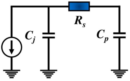
Figure 12.
RC equivalent circuit for the Ge-on-Si PD in [33].
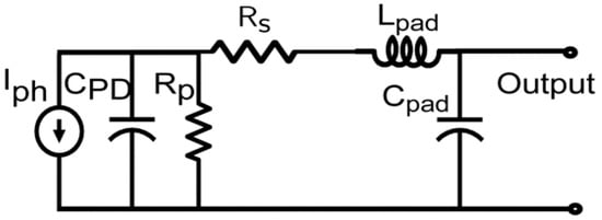
Figure 13.
Equivalent circuit of the UTC PD in [50].
A more involved RF small-signal equivalent PD circuit is presented in Figure 14 [77], where the transit time and the RC time effects are included. It can be seen that the input voltage source represents the input radio-frequency optical power component, followed by the PD transit-time equivalent circuit, including and , where their values are optimized initially to characterize the PD transit-time bandwidth correctly. The transit-time bandwidth is usually very high, with values that could reach around or more. Therefore, it can be ignored when the targeted operating frequencies are well below 100 GHz. The output voltage represents the generated RF electric field in the PD absorption region, which drifts the free carriers to the PD external circuit. Therefore, the PD photocurrent is represented by the voltage-dependent current source , which is dependent on the generated RF electric field in the PD absorption region and the PD responsivity . The PD photocurrent feeds the RC-time equivalent circuit and the PD load. The PD equivalent circuit in Figure 14 provides a more accurate frequency response for the photodiode. It is worth highlighting that the space-charge effects and thermal failure limit the output RF power from the photodiode. When the photodiode is operated under low-power conditions, the photodiode operates in its linear region since the electric field in the depletion region is not collapsed and free carriers drift with constant saturation velocity; as a result, the PD equivalent circuit is independent of the input optical power. On the other hand, the equivalent circuit is dependent on the input optical power when the photodiode is operated under high-power conditions because the PD transit-time and junction capacitance become dependent functions of the input optical power; as a result, the output RF power varies nonlinearly with the input optical power.
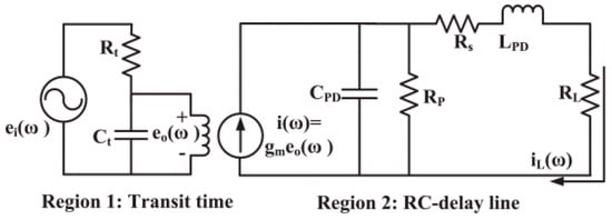
Figure 14.
Photodiode equivalent circuit including the transit time and RC time effects [77].
It is important to highlight that the presented PD equivalent circuits in Figure 12, Figure 13 and Figure 14 do not include many crucial physical effects occurring under high-power and high-speed conditions. The presented equivalent circuits do not include space-charge effects and nonlinear velocity effects because they assume linear charge transport. However, at high optical power, space-charge effects occur due to the large numbers of generated electron-hole pairs. As a result, the electric field in the depletion region is decreased, causing the carrier velocity to decrease and the transit time to increase. In addition, the impacts of junction heating and thermal effects are not captured by the presented PD equivalent circuits because they employ temperature-independent elements. However, at high optical powers, heating in the Ge absorption region increases the dark current, changes the bandgap and reduces the carrier mobility. Also, phonon scattering increases at high temperatures, so the carriers lose energy more frequently. As a result, the saturation velocity decreases. The saturation velocity and mobility also decrease because of defects, dislocations and traps, which increase scattering rates. Mobility and saturation velocity decrease in this case because these impurities and defects limit how long carriers can accelerate between collisions. The PD equivalent circuits do not model these thermal effects impacts. Furthermore, the equivalent circuits do not model the saturation and nonlinear photocurrent response occurring at high optical powers due to space-charge effects, carrier recombination, and Avalanche effects. This is because the current source in the equivalent circuit is linearly proportional to the optical power. In addition, at high-speed operations, the photodiode tends to behave like a distributed element, especially if it is designed with a large area or is wire-bonded. Therefore, parasitic inductance and parasitic capacitance (limiting the PD bandwidth) due to packaging or tracing are introduced. These parasitic inductances and capacitances are not modeled in the PD equivalent circuits. As a result, these equivalent circuits are not sufficient for S-parameter representation. Also, the series resistance in metal contacts and semiconductor layers at high photocurrents becomes significant, introducing voltage drops that limit the PD bandwidth and dynamic range. The PD equivalent circuits do not model distributed or temperature-dependent series resistance. Also, the PD equivalent circuits do not model the Avalanche or tunneling effects at high bias and do not include the multiplication noise, excess noise factor, or nonlinear breakdown behavior. The high reverse bias causes impact ionization (Avalanche effect) and tunneling current, especially in Ge with a narrow bandgap. These effects are not modeled by the PD equivalent circuits presented in Figure 12, Figure 13 and Figure 14. Furthermore, at very high frequencies, the PD equivalent circuit will fail to represent the PD performance. It is also, at this point, worth linking the PD equivalent circuit elements with system-level requirements. The photocurrent source in Figure 13 is proportional to input optical power and PD responsivity; the junction capacitance in Figure 13 limits PD speed and depends on bias voltage and PD area; the series resistance in Figure 13 is the contact resistance and highly doped semiconductor layer resistance; the shunt resistance in Figure 13 models the dark current paths, and the parasitic elements and in Figure 13 model the bond wires and PD pads, and they limit the RF performance. controls the PD bandwidth, the PD bandwidth is increased when is decreased. controls the PD responsivity and bandwidth, the voltage drop on increases when is increased, resulting in a lower voltage appearing on the load, reducing the output voltage or current swing. The shunt resistance controls the PD noise and dark current. The dark current, PD noise and false signals increase when is lower. The parasitic elements and control the RF bandwidth performance and limit the impedance matching between the PD and the load. and should be minimized for higher bandwidth. Therefore, a smaller active area and a higher bias should be applied. and should also stay constant at high photocurrents to obtain higher PD linearity. In addition, the PD saturation current region should be avoided for higher linearity. Lower PD noise can be obtained when is higher, which results in a smaller dark current and minimized shunt and thermal noise. The PD power handling is higher by avoiding thermal runaway and saturation of the source. Lower jitter and stable edge response are achieved when is stable and minimal parasitics are obtained. The PD sensitivity is higher when the PD responsivity is maximized, and dark current and noise are minimized.
The PD nonlinearities and the thermal effects have important impacts on the equivalent circuit elements and carrier transit time. The PD nonlinearity is a function of reverse bias, input optical power, photocurrent, operating frequency, and temperature. The PD bandwidth is dependent on the reverse bias because the electric field across the PD junction is proportionally dependent on the reverse bias, and the electron and hole drift velocities in the depletion region are proportionally dependent on the electric field. Therefore, the electron and hole drift velocity increase when the reverse bias increases, the carrier transit time decreases, and the PD bandwidth is consequently enhanced. In addition, the depletion region width increases when the reverse bias increases, causing the PD bandwidth to be improved. At high optical powers, the PD bandwidth is also dependent on the input optical power because of space-charge effects induced by large photogenerated carrier density in the depletion region that introduces an electric field opposing the internal electric field in the depletion region. As a result, the carrier drift velocity in the depletion region decreases, and the PD bandwidth is degraded. In addition, when the input optical power is high, the voltage drop across induces accumulation of free charges on both edges of the depletion region. Hence, an additional capacitance is induced, which increases the junction capacitance (degrading the PD bandwidth) and makes the junction capacitance dependent on the input optical power. Also, increases due to space-charge effects because the depletion width reduces. The carrier transit time increases due to the space-charge effects. The dark current also increases due to the space-charge effects and recombination, causing the shunt resistance to decrease. In the PD linear region, the electric field in the depletion region is not counteracted, free carriers drift with constant saturation velocity, and the PD responsivity, transit time, total resistance, and junction capacitance are constant and independent of the input optical power. As a result, the photogenerated RF power increases linearly with the square of the input optical power; i.e., the PD transfer function is independent of the input optical power. The maximum output of photogenerated electrical power at PD saturation is limited by space-charge effects and thermal failure. In the PD nonlinear saturation region, at high optical power operations, the PD transfer function is dependent on the input optical power, with the PD responsivity, transit time, total resistance, and junction capacitance dependent on the input optical power and bias voltage. As a result, the output photogenerated electric power changes nonlinearly with the square of the input optical power. In addition to space-charge effects, carrier velocity saturation, nonzero load resistance, scattering, recombination and trap sites contribute to the PD nonlinear behavior. In addition, the PD charge distribution, electric field distribution, and transition velocity (dependent on the input optical power) are non-uniform for HPHS PDs, contributing to the PD nonlinear behavior. The carrier velocity saturation causes the series resistance to increase due to increased heating and the transit time not to decrease. On the other hand, the thermal effects degrade the HPHS PD performance. Higher output RF power, higher saturation photocurrent, wider PD bandwidth, and better PD dynamic range can be obtained when the thermal effects are mitigated. The thermal effects increase at high power conditions and high reverse bias. At high PD temperatures, phonon scattering increases, carriers lose energy more frequently, and their mobility decreases; as a result, the PD saturation velocity decreases, consequently reducing the PD speed. In addition, the PD leakage current increases sharply with the temperature increase, causing the shunt resistance to decrease sharply. The series resistance increases because the resistivity of the metal and semiconductor increases with temperature increase. The PD responsivity changes with the increase in temperature because of bandgap narrowing.
It can be seen from Figure 15 and Figure 16 [35,78] that the PD equivalent circuit can also be designed, including the CPW line model, where the S-parameters of the CPW line are included in the CPW line model in the equivalent circuit. It can be seen from Figure 16 that the PD CPW line is designed with an inductive-peaking transmission line tapered to a line. Therefore, inductive peaking is employed to enhance the photodiode bandwidth.
Figure 15.
A more accurate PD equivalent circuit includes the full-wave simulated PD CPW pads [78].
Figure 16.
PD equivalent circuit including the simulated S-parameters of the PD CPW pads [20].
The equivalent circuit of the photodiode array, when it is composed of two elements, is presented in Figure 17 and Figure 18b [36,40]. It can be seen from Figure 17 and Figure 18b that the PD bandwidth is not decreased when two array elements are implemented because the two Ge regions are connected in parallel, and while the total junction capacitance is doubled, the total photodiode resistance is halved at the same time. As a result, the bandwidth of the PD array with two elements does not decrease when compared with the corresponding single-element PD bandwidth. This fact is obvious from Figure 18b, where it can be seen that the junction capacitances of the two Ge regions and the element resistances are connected in parallel. The shunt topology in Figure 18b is chosen because the two Ge regions are connected in parallel as presented in Figure 17. It can be seen from Figure 17 that the PD element junction is available in the Ge region, and the top N++ Ge regions of the two elements are connected to the same ground electrode, while the P++ Si region of the two elements is connected to the same signal electrode. As a result, the two Ge regions are connected in parallel.
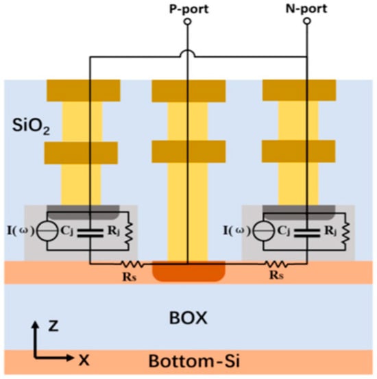
Figure 17.
RC equivalent circuit for the PD array in [36].
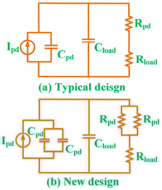
Figure 18.
(a) Equivalent circuit for a single-element PD and (b) equivalent circuit for a two-element PD array [40].
On the other hand, when the PD array is composed of more than two elements connected in parallel, as shown in Figure 19 [41], the bandwidth of the PD array is decreased. This is because the elements’ resistances and junction capacitances, and in Figure 19, are not connected in parallel, and this equivalent circuit should be analyzed using different mathematical approaches to find the PD array bandwidth; e.g., the transmission matrix method can be used to find the frequency response of the PD array with more than two elements. The power loss in the PD array with more than two elements will also increase. However, the overall saturation photocurrent increases sharply as the number of elements increases.
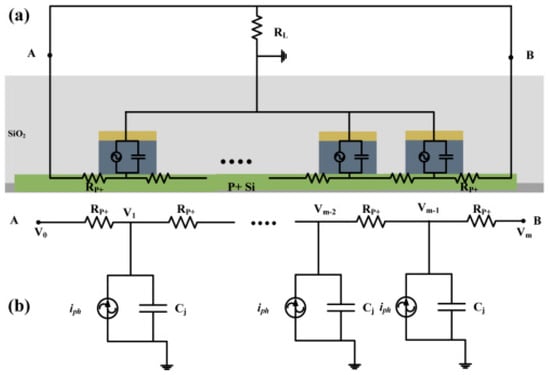
Figure 19.
Equivalent circuit for the n-element PD array in [41]. (a) The cross-section view and equivalent circuit of n-cell DAPD; (b) the equivalent circuit extracted from points A to B.
2.3. Photodiode Bandwidth Design
The electrical 3 dB bandwidth of the photodiode is dominantly limited by the RC-time and transit-time bandwidths. The photodiode equivalent circuit can provide the RC- and transit-time bandwidths. The carrier transit-time bandwidth for the Ge-on-Si PD in [33] was calculated as shown in Equation (1),
where is the carrier drift velocity, and is the thickness of the Ge region. The carrier drift saturation velocity depends on the electric field strength; it is for the Ge medium [33]. The carrier transit time can be defined as the required time for the photogenerated electrons and holes to travel from the absorption region to the collecting electrical electrodes. The holes’ drift velocity dominantly limits the transit-time bandwidth for Ge-on-Si photodiodes because the holes are slower than electrons. On the other hand, the RC-time bandwidth was found to be calculated as shown in Equation (2) [33,36],
where is the total PD resistance, including the PD series ohmic-contact resistance, junction resistance, and load resistance, and is the total PD capacitance, including the junction and parasitic capacitances. If the load resistance is set to zero, then the resistance can be found as shown in Equation (3) [33],
where is the PD junction resistance, and is the series contact resistance. The junction capacitance can be found as shown in Equation (4),
where is the dielectric constant of the Ge medium, is the PD active area, and is the depletion region depth.
The overall electrical 3 dB bandwidth can be obtained as shown in Equation (5) [33].
The RC-time bandwidth dominantly determines the electrical 3 dB low-pass bandwidth of the photodiode if the Ge thickness is small and the frequency of operation is not too high. It is worth highlighting the trade-off between the transit- and RC-time bandwidths. When the Ge thickness is decreased to improve the transit-time bandwidth, the RC-time bandwidth is degraded, and vice versa. In addition, the photodiode bandwidth, saturation RF power, and PD linearity are dependent parameters on the bias voltage and input optical power. The junction capacitance varies when the bias voltage changes because the PD depletion region width varies. As a result, the RC-time bandwidth is varied. On the other hand, when the input optical power increases, the space-charge effects increase, and the electric field in the absorption region decreases; as a result, the carrier velocity decreases and the transit-time bandwidth decreases.
The RC bandwidth of the PD array of two elements is equal to the RC bandwidth of the single-element PD. This part proves this concept mathematically. The RC-time bandwidth of the single-element PD can be written as shown in Equation (6) [40].
And the RC-time bandwidth of the two-element PD array is shown in Equation (7) [40].
It can be seen from Equations (6) and (7) that the total resistance of the PD array is divided by 2, and its total capacitance is multiplied by 2 because the two Ge regions are connected in parallel. Therefore, it can be seen from Equations (6) and (7) that the RC bandwidth of the two-element PD array is almost equal to the RC bandwidth of the single-element PD. However, when the number of array elements is more than two, the PD array bandwidth decreases as the number of elements increases.
The mmWave Frequency Range 2 (FR2) band used in 5G/6G has high bandwidth requirements due to the extremely high carrier frequencies involved. The FR2 band covers the frequency range from 24.25 to 71 GHz, where the required bandwidth per channel is 100–400 MHz for basic 5G NR mmWave applications, 800 MHz to 2 GHz for high-performance mmWave applications, and 5–10 GHz for advanced 6G research applications. Therefore, the antennas or antenna arrays used for the FR2 band should have operating bandwidths of more than 5 GHz, and the photodiode with the trans-impedance amplifier (TIA) should have a bandwidth that is more than 20–40 GHz such that it is possible to achieve a 64QAM or 256QAM modulation scheme, for example. Also, these photodiodes implemented for RoF or electro-optic links for the FR2 band must have high linearity performance to support complex modulation schemes and minimize noise and nonlinearity over the entire mmWave Intermediate Frequency (IF) range. On the other hand, the frequency bands higher than 100 GHz, including the frequency range from 100 GHz to 1 THz, are employed for future 6G, ultra-high-speed wireless backhaul, and chip-to-chip communication. The expected bandwidth requirements for this high-frequency range are 10–100 GHz per link for 6G THz wireless applications, 10–20 GHz per channel for wireless backhaul/fronthaul applications, 50–100 GHz per link for chip-to-chip communications, 10–30 GHz for radar/sensing/imaging applications, and 50 GHz for ultra-high-definition (HD) holography/extended reality (XR)/augmented reality (AR) applications. These bandwidths are very wide because they are required to increase the communication data rates to achieve Tbps rates. The higher carrier frequencies are utilized because of more spectrum availability, and because the smaller wavelengths allow tighter spatial reuse. The antennas or antenna arrays operating for these future frequency bands will be required to be ultra-broadband with bandwidths of more than 50 GHz, and the photodiodes will be necessary to have bandwidths between 50 and 100 GHz. Therefore, the photodiode bandwidth should cover the target performance metrics for 5G/6G RoF systems operating in C-band. The photodiode must be fast enough to handle modulation up to the highest carrier frequency and bandwidth for mmWave FR2 and 6G THz bands. Hence, the PD RC bandwidth in Equation (2) should be enhanced by reducing the PD capacitance and series resistance. The PD capacitance can be reduced using a smaller PD area and thicker junction, and the series resistance can be reduced using good contacts and shorter interconnects. The transit time bandwidth in Equation (1) can be enhanced by reducing the absorber thickness, using higher electric fields to reach saturation velocity, or using materials with higher saturation velocity. In addition, high absorption must be maintained for the PD responsivity to be higher. Therefore, resonant or enhanced absorption using plasmonics or Guided-Mode Resonance (GMR) is utilized to allow thin absorber implementation. Also, the PD should have high linearity performance by minimizing the space-charge effects. As can be seen from the 6G RoF system requirements, the PD speed and power need to be improved using different performance enhancement approaches such as plasmonics and resonance phenomena. The Guided-Mode Resonance (GMR) was used to enhance the Ge-on-Si PD bandwidth in [36] to 31.6 GHz, improve PD responsivity and photocurrent in [39], improve the PD bandwidth to more than 40 GHz and responsivity to 0.68 A/W [68], and improve the PD bandwidth to more than 60 GHz in [79]. Plasmonics were also used to improve the PD speed and power performance. The Ge-on-Si PD responsivity was sharply enhanced thanks to using plasmonic structures in [80,81]. Plasmonic structures were also used to improve the photocurrent of Ge-on-Si PD by 13-fold [82,83].
2.4. Photodiode Saturation Current, RF Power, and Signal-to-Noise Ratio
The photocurrent versus optical power characteristics of this proposed PD in [63] show that three photodiode operation regions can be deduced, as shown in Figure 20. The first operation region is obtained where the photocurrent is linearly increased versus the input optical power because the PD is not saturated yet. The second operation region is obtained where the photocurrent increases linearly with the input optical power but with a different slope. The PD in this operation region is partially saturated, and the saturated PD volume increases with the increase in input optical power. The third operation region is the saturation region, where the PD is fully saturated, and as a result, the photocurrent does not increase when the optical power increases.
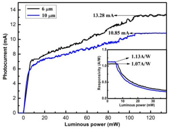
Figure 20.
Photocurrent versus optical power characteristics for the proposed PD in [63].
In general, the output RF photogenerated power can be found in using Equation (8). In addition, the saturation current, which starts in the nonlinear operation region, can be defined as the average photocurrent at which the RF power compression curve drops by 1 from its peak value.
It is worth noting that the PD power handling capability and saturation performance can be significantly improved when the incident light field is illuminated on the double sides of the Ge absorption region using different optimized manipulation approaches to allow the absorption profile to spread more uniformly across the PD absorption region. Different light manipulation approaches are proposed in [66], as shown in Figure 21. Type B PD has three sections, where Section 1 is used to generate multimodes, and the light is manipulated to provide a good pattern before reaching the Ge region. Section 2 allows the light to be illuminated in the front and side parts, which results in an optimized light distribution and a new absorption profile in the Ge region. Section 3 is designed so that the light is fully absorbed. Type B PD is modified to be double-sided illuminated using a MMI (MultiMode Interferometer) splitter shown as type C PD in Figure 21. It was found that the dark current for the three types is almost the same. The saturation current increases sharply from type A to type C, and the PD bandwidth increases sharply under high-power operations. The low-power operations bandwidth does not vary much when going from type A to type C PD.
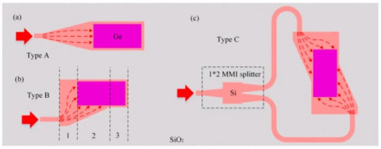
Figure 21.
Different optical field manipulation techniques, proposed in [66]. (a) Conventional fed Ge-on-Si PD. (b) Ge-on-Si PD with modified single-side optical illumination. (c) Ge-on-Si PD with modified double-sides optical illumination.
The total noise of a Ge-on-Si PD is the result of thermal noise, the shot or dark current noise, excess noise, and generation-recombination (quantum) noise [84,85]. The thermal noise occurs due to the thermal excitations of electrons of an electric conductor at equilibrium. The dark current noise is due to the current flowing in the bias circuit in the absence of light, and it is generated due to the lattice mismatch between Ge and Si and the valence band discontinuity. The excess () noise is negligible at high-frequency operations, and the quantum noise occurs due to the statistical nature of the production and collection of photoelectrons when an optical signal is incident on the PD [84,85]. Therefore, the total noise of the PD can be calculated as shown in Equation (9) [85],
where is the total RMS PD noise current, is the RMS quantum noise current, is the RMS dark current noise, and is the RMS thermal noise current, which can be found using Equations (10)–(12),
where is the electron charge, is the PD photocurrent at the operating angular frequency, is the angular frequency, is the Noise Equivalent Bandwidth (NEB), is the PD dark current, is the Boltzmann constant, is the temperature in Kelvin, and is the load resistance. The Noise Equivalent Bandwidth can be calculated using Equation (13),
where is the PD photocurrent at DC. Assuming that the PD frequency-dependent photocurrent current is a linear function with the DC photocurrent and the photocurrent at the 3 dB frequency point is , then the PD photocurrent can be written as shown in Equation (14),
where is the 3 dB frequency bandwidth of the photodiode. Taking the integral of Equation (14) (after being squared as shown in Equation (13)) with the integral limits from 0 to , the Noise Equivalent Bandwidth can be found as shown in Equation (15),
where is defined as shown in Equation (16),
Therefore, the total noise of the PD can be found when is found.
Now, using Equations (8) and (9), the PD Signal-to-Noise Ratio (SNR) can be found using Equation (17), which was used to calculate the PDs SNRs presented in Table 2.
It is good to highlight that the PD thermal and shot noise depend on the applied reverse-bias voltage. The thermal noise decreases as the bias voltage increases, and the shot noise increases as the bias voltage increases. Therefore, a minimum total noise is expected. The shot noise determines the PD noise at high operating frequency and high input power. On the other hand, the PD noise is determined by the thermal noise when the input power is low. Also, the NEB increases when the applied bias is low because the carriers trapping impact due to the band discontinuity is high, and the NEB saturates and does not change at high bias voltage because the trapping effect is sharply reduced. In addition, NEB reduces with an increase in the PD active layer thickness because NEB becomes transit-time limited instead of RC-time limited. Therefore, the PD active layer thickness should be optimized to minimize the PD NEB and maximize the PD bandwidth.
3. Photodiode Integrated Photonic Applications
3.1. MMWave Matching Network Design
The photodiode is a capacitive source, and an inductive matching network must be designed between the photodiode and the microwave load. The matching network can be designed directly on the photodiode substrate or a separate substrate where wire or flip-chip bonding connects the matching network to the photodiode. A microwave load is designed with an input impedance of ; however, this impedance is low, degrading the photodiode sensitivity because of high thermal noise and weaker absorption for the RF photogenerated power. The photodiode matching network uses three approaches to achieve complex conjugate matching between a photodiode and a microwave load. First, a matching network is designed between the photodiode and a microwave load. This matching network uses spiral inductors, quarter-wavelength transformers, matching open- or short-circuited shunt CPW stubs, and inductive peaking transmission lines. The inductive peaking transmission line is designed to have a very high characteristic impedance tapered to a low characteristic impedance line to be matched with the microwave load input impedance. The inductive peaking transmission lines are also used to improve the photodiode bandwidth. Second, the antenna input impedance is engineered to achieve an inductive reactance that slowly varies with frequency. The third approach is realized when a Trans-Impedance Amplifier is used to achieve the impedance matching between a photodiode and a microwave load.
The first approach is shown to be used in Figure 22, where resonating mmWave matching networks are presented [86,87]. These resonating matching networks provided a narrow matching bandwidth. It can be seen from Figure 22 that these matching networks are composed of CPW quarter-wavelength transformers and inductive peaking lines. It can also be seen that DC block capacitors are used so that the RF signal is blocked from flowing to the DC bias network and forced to flow into the microwave load.
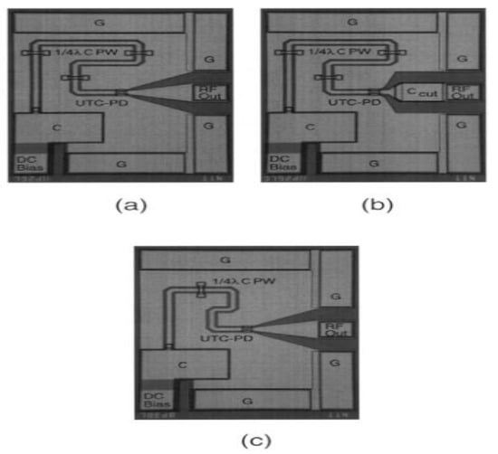
Figure 22.
Micrographs of the fabricated photonic microwave generators (PMGs) presented in [86,87]. (a) PMG with topology-A, (b) PMG with topology-B, and (c) PMG with topology-C.
The second matching approach can be seen in Figure 23 and Figure 24, where the antenna input impedance is inductive and compensates for a photodiode’s capacitive reactance [88,89]. The antenna geometrical parameters are optimized to achieve the complex conjugate matching between the photodiode and the antenna. The Connected-Array antenna of bowtie elements is designed on an Aluminum Nitride (AlN) substrate [88]. The substrate thickness and dielectric constant of the AlN substrate were optimized to control the antenna input real-part impedance, while the input inductive reactive impedance was attained using the inductive peaking technique using a coplanar strip line and wire bonds (as shown in Figure 23). Furthermore, the antenna metallic dimensions can be optimized to achieve the complex conjugate matching as shown for the proposed Short Asymmetric Inductive Dipole (SAID) antenna in [89], as shown in Figure 24. The proposed photonic antenna in [89] has a reconfigurable bandwidth in the frequency range from to . The antenna input real-part impedance was controlled using the ground and dipole dimensions, as well as the proximity spacing between the dipole and ground. On the other hand, the antenna input inductive imaginary-part impedance was attained using the two metallic loops around the feeding CPW pads. Figure 25 presents the output impedance of the UTC PD at different bias voltages and the antenna input impedance, in addition to the return loss for the antenna with respect to the PD output impedance [89].
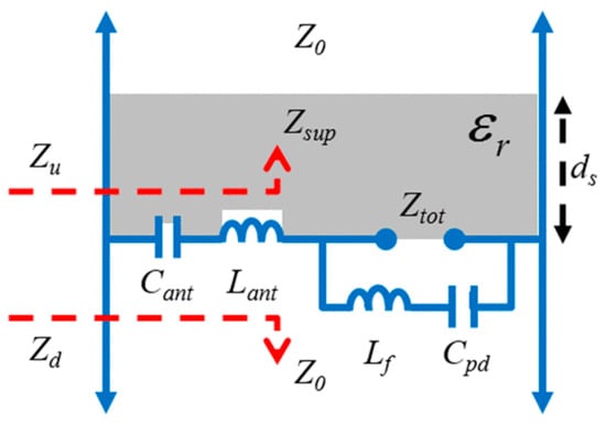
Figure 23.
Circuit model for the photonic-integrated Connected Array antenna in [88].
Figure 24.
Proposed photonic-integrated SAID antenna in [89].
Figure 25.
(a) Real-part output impedance for the UTC PD at different bias voltages and Reconfigurable Antenna (RA) real-part input impedance, (b) imaginary-part output impedance for the UTC PD at different bias voltages and Reconfigurable Antenna (RA) imaginary-part input impedance, and (c) the return loss for the Reconfigurable Antenna with reference to UTC PD output impedance at different bias voltages [89].
The third impedance-matching approach is implemented using a Trans-Impedance Amplifier [90], as shown in Figure 26. It can be seen from Figure 26 that three transistors are used to step up the photodiode low output impedance to . Unfortunately, this transimpedance amplifier consumes a lot of power and achieves a narrow matching bandwidth.
Figure 26.
Transimpedance low-noise amplifier in [90].
The resonant mmWave matching networks increase the PD output power at the resonant frequency, and they match the PD with the mmWave load for narrow bandwidths. The resonant mmWave matching networks could achieve 77% 3 dB bandwidth percentage of the resonant frequency [86,87]. In addition, the resonant mmWave matching networks provide a compact size and easy integration with the PD and mmWave load. On the other hand, more compact matching networks with easier integration are obtained when the mmWave antenna input impedance is engineered to achieve complex-conjugate matching with the PD output impedance. The 3 dB bandwidth percentage reaches 83% when a traveling wave antenna is used [88], and a smaller—10 dB bandwidth percentage of 20% is obtained when a resonant mmWave antenna is employed [89]. The Trans-Impedance Amplifier (TIA) in [90] could provide a 3 dB bandwidth percentage of 9.5% at 60 GHz, which is much lower than the bandwidth percentages achieved by the resonant mmWave matching networks and the antenna design. In addition, the integration of the TIA with the PD and antenna is complex and provides bulky matching networks. In addition, the power consumption of the TIA is high; e.g., it is 30 mW for the TIA in [90]. Therefore, it is preferable to implement the passive mmWave matching networks or optimize the mmWave antenna parameters to achieve impedance matching between the PD and the mmWave antenna. Hence. The passive matching networks or antenna input impedance should be very inductive to strongly absorb the RF photogenerated current and direct it to the antenna to radiate into space.
Furthermore, the photonic matching network should incorporate a bias tee such that the photodiode is DC reverse biased, and the RF signal is blocked from flowing to the DC biasing network [91,92]. The DC bias is blocked from flowing into the RF load using an interdigital capacitor as shown in Figure 27 and Figure 28. On the other hand, the RF signal is isolated from flowing into the DC biasing network using a grounded CPW open-circuited shunt stub as shown in Figure 27, or using a band-reject filter as shown in Figure 28. The proposed bias tee in [91] was designed to operate in the frequency band from to while the bias tee in [92] operates from to
Figure 27.
GCPW bias tee in [91].
Figure 28.
GCPW bias tee in [92]. (a) Band-reject filter to block RF signal. (b) Interdigital capacitor to block DC signal.
3.2. Photodiode Integrated Photonic Emitters
A photonic-integrated quarter-wavelength monopole antenna was designed at 15 GHz on a Silicon chip with a volume of , a gain of , and a bandwidth of [93]. The proposed design is shown in Figure 29. The photodiode is connected at the GSG pads shown in Figure 29, where the photodiode is a Ge-on-Si photodiode designed to be operated under low-power conditions.
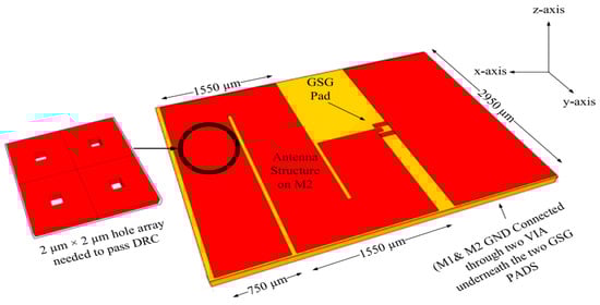
Figure 29.
SiPh monopole antenna in [93].
The proposed photonic antenna in [94] was designed in the bandwidth 3.3–3.7 GHz with two matching approaches. The first approach involves matching the photodiode to and designing the antenna to be well matched to Then, the photodiode with its matching network is connected to the antenna. The second approach used the antenna input impedance to achieve complex conjugate matching with the photodiode output impedance. The proposed photonic antenna in [94] is shown in Figure 30. The output RF current from the photodiode is fed to a patch antenna using a probe feed that goes through an air-filled cavity. The bottom face of the air-filled cavity includes a slot element that divides the cavity into two coupled half-mode cavities and excites the patch antenna. Therefore, two modes are excited to widen the operating bandwidth.
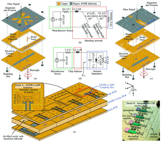
Figure 30.
Photonic-integrated slot antenna in [94]. (a) The photonic integrated single-element slot antenna, (b) the equivalent circuit for the single-element slot antenna, (c) the conjugate-matched single-element photonic antenna, (d) the equivalent circuit of the conjugate-matched single-element antenna, and (e) four elements of a photonic antenna array and an image for the active array.
The proposed photonic antenna design in [95] accomplished the complex conjugate impedance matching using the antenna geometry optimization. The proposed photonic antenna in [95] is shown in Figure 31. The antenna is a Short Asymmetrical Inductive Dipole (SAID) antenna achieving a low cross-polarization level, high radiation efficiency, a bandwidth from to , and a frequency reconfigurability feature when the photodiode reverse bias voltage is varied. Two parallel folded dipoles are used to achieve an impedance transformation and a slowly varying input impedance with respect to frequency. The antenna theory of operation was explained using the Transmission-Line Mode (TLM) and Radiating Mode (RM). As a result, the characteristic impedance of the Transmission-Line Mode stub and the radius of an equivalent dipole for the proposed antenna can be obtained. Therefore, the antenna input impedance is found considering that the antenna is composed of two parallel monopoles with a lower truncated arm. It was found that the antenna input impedance incorporates a step-up impedance ratio, the impedance of the parallel monopoles, and the coplanar short-circuited stub impedance. Therefore, the real-part of the antenna input impedance was contributed using the TLM, and the imaginary part was contributed using the RM.
Figure 31.
Short asymmetrical inductive dipole antenna in [95].
The work in [96] also integrated an mmWave antenna at 100 GHz with two UTC photodiodes, as shown in Figure 32. The RF signal is fed into the radiating antenna aperture using a coupling slot to block the DC signal from flowing to the radiating antenna. It can be seen from Figure 32b that the antenna radiating aperture is made of symmetrical modulated Metasurface arrays, which are fed using out-of-phase RF fields. The Metasurface array comprises a capacitive impedance boundary condition sinusoidally modulated along the field propagation direction. The inductive boundary condition is also obtained by using an inductive grounded substrate. Therefore, transverse-magnetic surface waves propagate and radiate because of the periodic modulation.
Figure 32.
(a) Top view of the proposed photonic modulated MTS array antenna in [96], and (b) four modulated MTS subarrays.
The photonic-integrated antenna at , as shown in Figure 33, was designed to achieve beam steering [97]. The radiating structure is composed of two stacked patches on a single-mode cavity to achieve a wide operating bandwidth. It can be seen that the RF signal propagates through Substrate Integrated Waveguides (SIWs) to finally couple to the radiating structure. The array grating lobes are reduced using eight elements along the antenna H-plane and two elements along the E-plane. This proposed array is connected to a UTC photodiode, and the beam steering is realized using optical phase shifters.
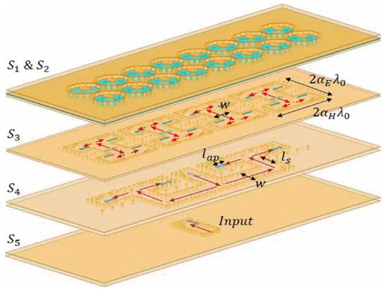
Figure 33.
Photonic-integrated subarray antenna in [97].
The photonic-integrated antenna array in [98] was designed to operate in the frequency range from to using a single-element Leaky-Wave antenna with beam steering occurring with respect to the operating frequency. The proposed photonic Leaky-Wave antenna array is shown in Figure 34, where it can be seen that two UTC photodiodes are used to feed the antenna array. The single-element Leaky-Wave antenna comprises four periodic unit cells connected in series to a microstrip line and a patch element attached at the antenna end. The proposed unit-cell is also presented in Figure 34. It comprises four half-wavelength open-circuited shunt stubs that introduce high-impedance points along the microstrip line. Therefore, the high-impedance points perturb the propagating electromagnetic waves, and signal reflections and losses occur. The single-element Leaky-Wave antenna is optimized to minimize reflections and maximize radiation, and the remaining waves reach the antenna end and radiate by the patch. This proposed Leaky-Wave antenna array obtained a directivity of , and a frequency beam-scanning range of 22°.
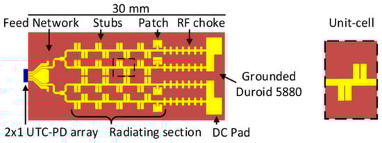
Figure 34.
LWA array in [98] and the unit-cell of the radiating section.
The proposed photonic two-element array in [99,100] used a traveling-wave antenna because of its slowly varying input impedance versus frequency. The proposed array is shown in Figure 35, where it can be seen that it is composed of two array elements. The proposed antenna array provided a gain of in the operating bandwidths from to and from to It was also found that the radiated power from the array is at
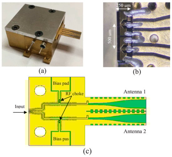
Figure 35.
Photonic-integrated antenna array proposed in [100]. (a) Packaged fabricated optical Tapered Slot antenna array. (b) wire-bonding from HPHS PDs to antenna CPW lines. (c) Top view of the optical Tapered Slot antenna array.
The Bowtie antenna was used to achieve a photonic-integrated antenna at [101], a photonic-integrated Connected Array antenna at 20 GHz [88], and a linear array at 50 GHz [102]. The proposed photonic-integrated Connected Array antenna shown in Figure 36 [88] presented a wideband of operation from to thanks to using the single-element Bowtie antenna. The four photodiodes are Charge-Compensated Modified UTC photodiodes with an output RF power of at for a single photodiode. Flip-chip bonding was used to connect the photodiode to the used Aluminum Nitride (AlN) substrate to increase the photodiode peak RF power. In addition, the PD coplanar strip output line and the wire bonds were used to increase the photodiode’s inductive load and improve the impedance matching. Tuning the thickness and dielectric constant of the used AlN substrate improved the impedance matching between the antenna and photodiode. It is worth noting that the small gap between adjacent Bowties works as a capacitive RF short between the array columns. Therefore, a current sheet is realized, which produces broadside radiation patterns. The proposed photonic Connected Array antenna was capable of steering the beam to The radiated power from the antenna was more than up to
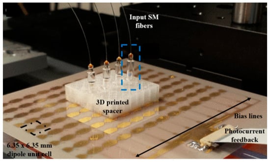
Figure 36.
CA antenna in [88] with four single-mode fibers and lenses connected to the active antenna elements.
Also, the coplanar-patch antennas at were connected to a photodiode [103,104]. It was found in [104] that the photonic-integrated coplanar patch, shown in Figure 37, has a gain of thanks to the inductive peaking matching technique and the low-loss AlN substrate used. While the coplanar-patch antenna, with bandwidth from to , in [103] obtained a gain of due to the use of a lossy Silicon substrate.
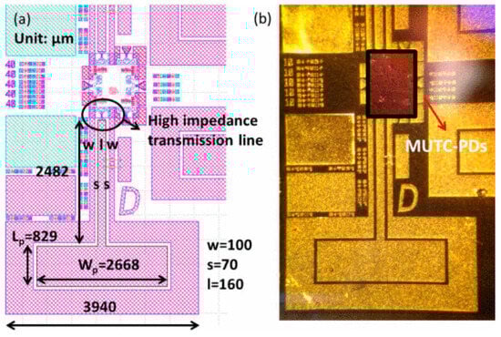
Figure 37.
Photonic coplanar patch in [104]. (a) Design of the optical coplanar-patch antenna. (b) microscopic picture for the optical coplanar-patch antenna.
The employed antennas for photonic-antenna applications are resonant antennas [93,94,95,97,101,102,103,104,105,106] or traveling wave antennas [88,96,98,100]. The resonant mmWave antennas such as monopole antenna [93,106], cavity-backed patch antenna [94,97], SAID antenna [95], Bowtie antenna [101,102], and coplanar patch antennas [103,104] provide narrow bandwidths for the optical antennas. On the other hand, traveling wave antennas such as the modulated Metasurface Array [96], Leaky-Wave antenna [98], Tapered Slot antenna [100], and Connected Array antenna [88] provide wide bandwidth optical antennas. Table 4 presents a comparative analysis between the presented resonant and traveling wave optical antennas. It compares the optical antennas’ gains, radiation patterns, antenna sizes, beam steering capability and optical integration complexity, as well as operating bandwidths.
Table 4.
Comparison table between the presented optical antennas.
It can be seen from Table 4 that the traveling wave antennas provide wider bandwidths, with bandwidth percentages reaching 75% [88], while the resonant antennas provide narrower bandwidths, with percentages reaching 21% [104]. The THz Bowtie antenna in [101] did not provide the impedance matching bandwidth but did provide the maximum frequency at which RF radiation takes place, and the monopole antenna in [106] did not provide the impedance matching bandwidth with respect to the PD output impedance. Monopole antennas suffer from low peak gains with omnidirectional radiation patterns that would complicate the accomplishment of beam steering. However, the monopole antennas are very easily integrated with the PD on the same chip. Compared to monopole antennas, coplanar patch antennas have improved peak gains, bandwidths, and directional radiation patterns if backed with a metallic reflector or ground plane. They are also easily integrated with HPHS PDs because they can be manufactured with the PDs on the same chip due to their very compact sizes. However, the requirement of adding a reflector to broaden the radiation patterns increases the complexity of optical integration. The cavity-backed patch antenna has more improved peak gain and directional radiation patterns, enabling the beam steering feature for its antenna array. However, the cavity-backed patch antenna is complicated to be integrated with the PD on the same chip, and flip-chip or wire bonding will be required. The SAID antenna achieved the best single-element antenna performance with the highest peak gain, directional radiation patterns, and compact size. Therefore, the SAID antenna can provide beam steering easily, and be integrated with HPHS PDs easily. The traveling wave antennas achieve wide operation bandwidth and can be optimized to achieve impedance matching with the PD without incorporating a matching network between the antenna and PD. However, they suffer from large sizes, making integrating directly with HPHS PDs on the same chip complicated, and flip-chip or wire bonding is required. The array antenna design enhances the peak gain sharply. However, the large sizes of the antenna arrays complicate the direct integration with HPHS PDs. Lenses can also increase the antenna gain sharply [101,102]. However, using lenses leads to complicated beam steering if achieved mechanically. The disadvantage of directly integrating the antenna with the PD on the same chip [93,103,106] is that the antennas suffer from low gains because of the lossy Si substrate. Therefore, using flip-chip bonding or wire bonding between HPHS PDs and antenna arrays would allow the antenna to have high peak gains with directional and steerable radiation patterns and wide operation bandwidth. The antenna should also be designed on substrates with high thermal conductivities (such as Aluminum Nitride (AlN)) to mitigate the HPHS PD thermal effects [88].
4. Future Trends and Challenges for C-Band HPHS Ge-on-Si RF Photodiodes
The thermal effects degrade the PD speed and power performance. Hence, many approaches are implemented to dissipate the heat effectively, especially when the PD is used under high power conditions. The optical light distribution in the PD absorption region should be uniform using the optical coupling techniques, allowing the light to transit gradually from the waveguide to the Ge region (such as the adiabatic coupling technique and evanescent coupling technique). Also, an optical dual-injection strategy, where the optical power is divided to feed the PD absorption region from both lateral sides, should be implemented to mitigate the thermal effects. The PD array design mitigates the thermal effects also, because the optical power is distributed between the single-element PDs, to provide HPHS PDs with a good PD performance. Fortunately, the Ge and Si materials have higher thermal conductivity than InP and InGaAs. Therefore, efficient and rapid heat dissipation occurs so the Ge-on-Si PDs can better manage the thermal effects [69]. Materials with higher thermal conductivities, such as Graphene and Graphene nanostructures, should also be employed for the PD design to alleviate the thermal effects. In addition, waveguide-coupled PDs are less sensitive to thermal effects because of independent paths of light absorption and carrier collection [69]. The PD should also be designed considering the trade-off occurring between the bandwidth and thermal effects. The PD with a smaller area obtains a wider bandwidth but higher thermal heating. However, the thermal effects can be sharply mitigated for normal-incident PDs with smaller areas when carefully designed mesa electrodes are used. Moreover, the thermal effects can be further mitigated by PD substrate thinning and decreasing the BOX layer thickness. These thermal effects degrade the PD speed because of reduced carrier saturation velocity, degrade the PD responsivity and saturation current because of reduced absorption and increased recombination, increase the dark current, which increases the PD noise and reduces the SNR, and degrade the PD linearity performance. Therefore, thermal simulations for the Ge-on-Si PD design should be performed to minimize the thermal effects, considering that the materials’ thermal conductivities degrade as the temperature increases. Thermal heating will mainly occur in the absorption region, which is mostly produced by photocurrent. Hence, the generated heat distribution follows the photocurrent generation distribution in the absorption region. Most heat leaves the depletion region in lateral directions, and the heat spreads when it flows downward into the P+-doped Si region and the buried oxide layer [48]. This buried oxide layer has low thermal conductivity that blocks the heat from being extracted [48]. Hence, its thickness should be reduced. The PD should be designed to minimize the thermal impedance from the depletion region to the heat sink. In addition, the PD thermal effects are mitigated when heatsinking is employed, where the PD is bonded to high thermal conductivity substrates such as Aluminum Nitride (AlN) or Diamond [45]. The thermal dissipation is also improved when high-quality thermal interface material is used between the PD and heat sinks [14]. In addition, the PD design should be optimized to reduce the transverse thermal impedance to avoid thermal runaway and mitigate the thermal effects.
The linearity for the HPHS Ge-on-Si PDs should also be high while maintaining broad-bandwidth and high-power features. Therefore, the space-charge effects and thermal effects should be minimized by achieving uniform optical distribution in the absorption region using waveguide-coupled and dual-injection techniques [33,35,36]. In addition, the carrier saturation velocity should be reached by carefully applying a higher reverse bias to maintain the PD’s wide bandwidth at high photocurrents. The PD thermal management should also be improved to avoid bandgap narrowing, carrier mobility degradation, and responsivity degradation with time, and enhance the PD linearity as a result. In addition, the PD doping profile could be optimized to improve the PD linearity and bandwidth [47]. When the doping profile is optimized, a higher electric field with higher uniformity is achieved in the absorption region, lower PD capacitance is obtained, and higher transit speed is utilized to enhance the PD linearity while preserving the PD speed. Advanced materials (such as GeSn) could also improve carrier mobility and tune the bandgap to obtain faster and more linear PDs [107]. Furthermore, the PD contacts and packaging should be designed to minimize parasitic series resistance and parasitic capacitance. In addition, using PD arrays dramatically enhances the PD linearity performance at wide PD bandwidth and high power.
The PD bandwidth could also be extended to reach frequencies well beyond 100 GHz for 6G technology. Different techniques, such as resonance phenomena and plasmonics, can enhance the PD bandwidth. The Guided-Mode Resonance using an optical structure, which is composed of a stack of and layers with periodic Si nanodisk arrays, was employed in the Ge-on-Si PD in [108] to enhance the light absorption, and consequently, the PD responsivity and photo-to-dark current ratio were improved. The PD bandwidth was improved to 250 GHz by thinning the absorption layer, and the optical structure is employed to compensate for the optical absorption degradation due to the thin absorber. Plasmonics were also applied on a Schottky PD to enhance the PD speed and photo-to-dark current ratio [109]. The Schottky barrier junctions provide ultra-high frequency response. The periodic plasmonic array was implemented on the metallic Schottky contact layer to confine the light in the depletion region and increase the light absorption. As a result, the PD photocurrent was enhanced with high-speed performance due to the Schottky barrier junction. Furthermore, the waveguide-coupled Ge-on-Si PD speed can be sharply improved to reach 260 GHz at a photocurrent of 1 mA [28]. The high-speed PD in [28] was capable of reaching 260 GHz and surpassing state-of-the-art III–V PDs because of the shortest transit times for photocarriers due to the employed biconcave form of the vertically aligned Ge fin with the narrowest Ge width in the center of the waveguide. This narrow Ge fin was sandwiched between two complementary in situ-doped Silicon layers.
There are also challenges related to the wafer-level testing for the combined photonic and RF performance. First, the RF signals at frequencies more than 40 GHz are sensitive to loss, parasitics, and impedance mismatch. Hence, the on-wafer GSG RF probes require precise calibration. In addition, de-embedding could also be necessary to remove the pad and probe effects. Second, the efficient optical coupling into and out of on-chip waveguides or photodiodes is difficult without packaging. Therefore, precise vertical or edge fiber alignment is required, and V-groove arrays, grating couplers, or micro-lens arrays are used for light coupling. It is a challenging task to maintain low coupling loss and to improve the optical coupling with polarization-sensitive couplers. Furthermore, high photocurrents and RF powers increase heating, and the wafer may not dissipate the heat quickly. As a result, the PD responsivity, linearity, and bandwidth are affected. The RF connections are also highly sensitive to discontinuities, parasitics, and poor ground referencing. In addition to the previously mentioned wafer-level testing challenges, it is also not easy to use the same experimental setup for simultaneous optical and RF measurements. These opto-electric measurement setups require much different equipment (including optical sources, RF signal generators, modulators, and high-speed equipment such as Vector Network analyzer and Bit-Error-Rate testers) that should be integrated. The measured results would also be impacted because of EM interference and cross-talk. In addition, the obtained optical and RF measurements would include parasitic effects of pads, probes, and cables; therefore, accurate modeling and de-embedding are important at high RF frequencies, and calibration short, open and matched loads are required to also be implemented on wafers. Moreover, for high-volume manufacturing, the optical alignment takes time, the RF probes require careful pressure and planarity, and manual probe wear and calibration drift affect repeatability. On the other hand, chip packaging is challenging to ensure 50 impedance matching between the on-chip RF connections and external RF circuits and to avoid RF cross-talk and EM interference. Also, the bond wire inductance or poor transition from the on-chip RF connections to coaxial connectors are challenges facing the PD packaging. Therefore, flip-chip bonding is preferred instead of wire bonding to minimize the parasitic inductance. Furthermore, many heating spots are generated, especially in dense packaging, when the PD operates under high power conditions. This poor thermal dissipation for PD packaging leads to performance degradation or failure and thermal expansion mismatch between the fiber and the chip. The PD packages also encounter vibration, humidity, and other mechanical effects. Therefore, ensuring that the fiber bonding is not disconnected or the RF connectors are not loosening or degrading are different challenges that must be overcome. Furthermore, when the PD is integrated with other integrated circuits or optical components in the package, parasitics and thermal load increase. As a result, the signal integrity across chip-to-chip links is degraded, and the thermal stability in dense electrical and optical input and output operations is also degraded.
Lastly, the design of Ge-on-Si PDs that withstand high optical power density and high electrical reverse bias, high photocurrent and high-speed signals over time is important for their reliable use in 5G and 6G technology and microwave photonics applications. There are many challenges facing the PD’s long-term reliability. The high photocurrents and absorbed optical power generate high amounts of heat in the PD, and consequently, the PD responsivity is degraded over time, the dark current increases over time, bandgap narrowing takes place, and carrier mobility degrades. Furthermore, the high carrier density induced by intense illumination distorts the internal electric field, causing carrier screening. As a result, the PD efficiency is reduced, and space-charge buildup is introduced, leading to increased nonlinearity. Also, thermal runaway could take place, which leads to thermal failure or early lifetime degradation. The PD material also changes over time due to stress, dopant diffusion, and interface degradation, especially for Ge-on-Si PD, where defect states and interfacial traps are more abundant. In addition, the high optical powers can excite nonlinear absorption and cause carrier trapping, heating, or bond breakage. Also, high current densities at metal-semiconductor contacts lead to interdiffusion, voids, or resistance increase and degrade the PD reliability, especially for PDs with fine-pitch RF pads.
5. Conclusions
The paper has reviewed the recent research on the design of high-power and high-speed SiPh Ge-on-Si photodiodes for RoF 5G communications applications. It has been indicated that the HPHS Ge-on-Si PDs are real candidates for the RoF-scheme 5G technology because these PDs have achieved sufficient RF photogenerated powers at mmWave frequencies. The principle and structure for the HPHS SiPh Ge-on-Si photodiodes have been introduced first. Then, the equivalent circuit model for the Ge-on-Si photodiode, enabling the calculation of the PD S-parameters and bandwidth, has been presented. After that, the PD transit-time and RC-time bandwidths were presented, and the impact of the linear PD array on the overall bandwidth was discussed. After that, the PD photocurrent behavior against the input optical power has been discussed. In addition, the RF photogenerated current mathematics and the optical signal manipulation techniques to improve the saturation current and bandwidth have been discussed. Lastly, the matching network design techniques to match the PD with mmWave antennas have been introduced, and the recent photonic mmWave antenna design has also been presented.
Author Contributions
Conceptualization, S.H.; methodology, software, S.H.; validation, S.H.; formal analysis, S.H.; investigation, S.H.; resources, S.H.; data curation, S.H.; writing—original draft preparation, S.H.; writing—review and editing, S.H., F.F., X.Z. and A.A.K.; visualization, S.H.; supervision, F.F., X.Z. and A.A.K.; project administration, F.F., X.Z. and A.A.K.; funding acquisition, F.F., X.Z. and A.A.K. All authors have read and agreed to the published version of the manuscript.
Funding
This work was supported by Fonds de Recherche du Québec–Nature et Technologie (FRQNT, Québec).
Data Availability Statement
All data are available within the manuscript.
Conflicts of Interest
The authors declare no conflicts of interest.
References
- Cisco Annual Internet Report (2018–2023) White Paper. Cisco, White Paper. Available online: https://www.cisco.com/c/en/us/solutions/collateral/executive-perspectives/annual-internet-report/white-paper-c11-741490.html (accessed on 18 July 2023).
- Nagayama, T.; Akiba, S.; Tomura, T.; Hirokawa, J. Photonics-Based Millimeter-Wave Band Remote Beamforming of Array-Antenna Integrated with Photodiode Using Variable Optical Delay Line and Attenuator. J. Light. Technol. 2018, 36, 4416–4422. Available online: https://ieeexplore.ieee.org/document/8328830 (accessed on 18 July 2023). [CrossRef]
- Siew, S.Y.; Li, B.; Gao, F.; Zheng, H.Y.; Zhang, W.; Guo, P.; Xie, S.W.; Song, A.; Dong, B.; Luo, L.W.; et al. Review of Silicon Photonics Technology and Platform Development. J. Light. Technol. 2021, 39, 4374–4389. Available online: https://ieeexplore.ieee.org/document/9380443 (accessed on 18 July 2023). [CrossRef]
- Shen, L.; Jiao, Y.; Yao, W.; Cao, Z.; van Engelen, J.P.; Roelkens, G.; Smit, M.K.; van der Tol, J.J.G.M. High-Bandwidth Uni-Traveling Carrier Waveguide Photodetector on an InP-Membrane-on-Silicon Platform. Opt. Express 2016, 24, 8290–8301. [Google Scholar] [CrossRef]
- Beling, A.; Campbell, J.; Li, Q.; Sun, K.; Wang, Y.; Wang, Z.; Yu, Q.; Zang, J. Modified UTC Photodiodes on Silicon for Low-Power High-Speed Applications. In Proceedings of the Photonics West 2018, San Francisco, CA, USA, 12 March 2018. [Google Scholar]
- Zeng, C.; Fu, D.; Jin, Y.; Han, Y. Recent Progress in III–V Photodetectors Grown on Silicon. Photonics 2023, 10, 573. [Google Scholar] [CrossRef]
- Beling, A.; Campbell, J.C. Heterogeneously Integrated Photodiodes on Silicon. IEEE Electron. Device Lett. 2013, 34, 319–321. Available online: https://ieeexplore.ieee.org/document/7273814 (accessed on 18 July 2023). [CrossRef]
- Xue, Y.; Han, Y.; Tong, Y.; Yan, Z.; Wang, Y.; Zhang, Z.; Tsang, H.K.; Lau, K.M. High-Performance III–V Photodetectors on a Monolithic InP/SOI Platform. Optica 2021, 8, 1204–1209. [Google Scholar] [CrossRef]
- Sun, K.; Jung, D.; Shang, C.; Liu, A.; Morgan, J.; Zang, J.; Li, Q.; Klamkin, J.; Bowers, J.E.; Beling, A. Low Dark Current III–V on Silicon Photodiodes by Heteroepitaxy. Opt. Express 2018, 26, 13605–13613. [Google Scholar] [CrossRef]
- Beling, A.; Xie, X.; Campbell, J.C. High-Power, High-Linearity Photodiodes. Optica 2016, 3, 328–338. [Google Scholar] [CrossRef]
- Roelkens, G.; Abassi, A.; Cardile, P.; Dave, U.; de Groote, A.; de Koninck, Y.; Dhoore, S.; Fu, X.; Gassenq, A.; Hattasan, N.; et al. III–V-on-Silicon Photonic Devices for Optical Communication and Sensing. Photonics 2015, 2, 969–1004. [Google Scholar] [CrossRef]
- Liang, D.; Bowers, J.E. Recent Progress in Heterogeneous III–V-on-Silicon Photonic Integration. Light Adv. Manuf. 2021, 2, 5. [Google Scholar] [CrossRef]
- Brouckaert, J.; Roelkens, G.; Van Thourhout, D.; Baets, R. Thin-Film III–V Photodetectors Integrated on Silicon-on-Insulator Photonic ICs. J. Light. Technol. 2007, 25, 1053–1060. [Google Scholar] [CrossRef]
- Gao, B.; Wang, H.; Liu, C.Y.; Meng, Q.Q.; Tian, Y.; Ang, K.S.; Si, J.H. Design and Analysis of InP-Based Waveguide Uni-Traveling Carrier Photodiode Integrated on Silicon-on-Insulator Through Al2O3 Bonding Layer. IEEE Photonics J. 2014, 6, 1–6. [Google Scholar] [CrossRef]
- Li, C.; Xue, C.; Liu, Z.; Cong, H.; Cheng, B.; Hu, Z.; Guo, X.; Liu, W. High-Responsivity Vertical-Illumination Si/Ge Uni-Traveling-Carrier Photodiodes Based on Silicon-on-Insulator Substrate. Sci. Rep. 2016, 6, 27743. [Google Scholar] [CrossRef]
- Zhou, Q.; Cross, A.S.; Yang, F.; Beling, A.; Campbell, J.C. Development of Narrowband Modified Uni-Traveling-Carrier Photodiodes with High Power Efficiency. In Proceedings of the Avionics, Fiber-Optics and Photonics Conference, San Diego, CA, USA, 1–3 October 2013; pp. 65–66. [Google Scholar]
- Zhou, Q.; Cross, A.; Fu, Y.; Beling, A.; Campbell, J.C. High-Power High-Linearity Flip-Chip Bonded Modified Uni-Traveling Carrier Photodiode. In Proceedings of the IEEE Photonics Conference (IPC) 2012, Burlingame, CA, USA, 23–27 September 2012. [Google Scholar] [CrossRef]
- Li, Z.; Fu, Y.; Piels, M.; Pan, H.; Beling, A.; Bowers, J.E.; Campbell, J.C. High-Power High-Linearity Flip-Chip Bonded Modified Uni-Traveling Carrier Photodiode. Opt. Express 2011, 19, B385–B390. [Google Scholar] [CrossRef]
- Xu, J.; Zhang, X.; Kishk, A. Design of High Speed InGaAs/InP One-Sided Junction Photodiodes with Low Junction Capacitance. Opt. Commun. 2019, 437, 321–329. [Google Scholar] [CrossRef]
- Li, Q.; Li, K.; Fu, Y.; Xie, X.; Yang, Z.; Beling, A.; Campbell, J.C. High-Power Flip-Chip Bonded Photodiode with 110 GHz Bandwidth. J. Light. Technol. 2016, 34, 2139–2144. [Google Scholar] [CrossRef]
- Wun, J.-M.; Lai, C.-H.; Chen, N.-W.; Bowers, J.E.; Shi, J.-W. Flip-Chip Bonding Packaged THz Photodiode with Broadband High-Power Performance. IEEE Photonics Technol. Lett. 2014, 26, 2462–2464. [Google Scholar] [CrossRef]
- Bowers, J.E.; Dai, D.; Zaoui, W.S.; Kang, Y.; Morse, M. Resonant Si/Ge Avalanche Photodiode with an Ultrahigh Gain-Bandwidth Product. In Proceedings of the 2010 IEEE Photonics Society Winter Topicals Meeting Series (WTM), Majorca, Spain, 11–13 January 2010. Paper WC2.2. [Google Scholar] [CrossRef]
- Bowers, J.E.; Dai, D.; Kang, Y.; Morse, M. High-Gain High-Sensitivity Resonant Ge/Si APD Photodetectors. In Proceedings of the Infrared Technology and Applications XXXVI, Bellingham, WA, USA, 3 May 2010. Paper 7660E-3H. [Google Scholar] [CrossRef]
- Zaoui, W.S.; Chen, H.-W.; Bowers, J.E.; Kang, Y.; Morse, M.; Paniccia, M.J.; Pauchard, A.; Campbell, J.C. Frequency Response and Bandwidth Enhancement in Ge/Si Avalanche Photodiodes with Over 840 GHz Gain-Bandwidth-Product. Opt. Express 2009, 17, 12641–12649. [Google Scholar] [CrossRef] [PubMed]
- Kang, Y.; Liu, H.-D.; Morse, M.; Paniccia, M.J.; Zadka, M.; Litski, S.; Sarid, G.; Pauchard, A.; Kuo, Y.-H.; Chen, H.-W.; et al. Monolithic Germanium/Silicon Avalanche Photodiodes with 340 GHz Gain–Bandwidth Product. Nat. Photonics 2009, 3, 59–63. [Google Scholar] [CrossRef]
- Assefa, S.; Xia, F.; Bedell, S.W.; Zhang, Y.; Topuria, T.; Rice, P.M.; Vlasov, Y.A. CMOS-Integrated High-Speed MSM Germanium Waveguide Photodetector. Opt. Express 2010, 18, 4986–4999. [Google Scholar] [CrossRef]
- Assefa, S.; Xia, F.; Vlasov, Y.A. CMOS-Integrated Low-Noise Germanium Waveguide Avalanche Photodetector Operating at 40 Gbps. In Proceedings of the Optical Fiber Communication Conference (OFC/NFOEC), Los Angeles, CA, USA, 21–25 March 2010. Paper OWN3. [Google Scholar] [CrossRef]
- Lischke, S.; Peczek, A.; Morgan, J.S.; Sun, K.; Steckler, D.; Yamamoto, Y.; Korndörfer, F.; Mai, C.; Marschmeyer, S.; Fraschke, M.; et al. Ultra-Fast Germanium Photodiode with 3-dB Bandwidth of 265 GHz. Nat. Photonics 2021, 15, 925–931. [Google Scholar] [CrossRef]
- Liu, Y.; Li, Z.; Atar, F.B.; Muthuganesan, H.; Corbett, B.; Wang, L. Integration of High-Performance InGaAs/GaN Photodetectors by Direct Bonding via Micro-Transfer Printing. ACS Appl. Mater. Interfaces 2024, 16, 10996–11002. [Google Scholar] [CrossRef]
- Huang, R.; Wang, Q.; Guo, Y.; Wang, Z. Comparative Study on GaAs/Si Heterojunction Fabricated by Nitrogen and Oxygen Plasma Activated Bonding. Vacuum 2023, 208, 111735. [Google Scholar] [CrossRef]
- Manda, S.; Matsumoto, R.; Saito, S.; Maruyama, S.; Minari, H.; Takachi, T.; Fujii, N.; Yamamoto, Y.; Zaizen, Y.; Hirano, T.; et al. High-Definition Visible-SWIR InGaAs Image Sensor Using Cu-Cu Bonding of III–V to Silicon Wafer. In Proceedings of the IEEE International Electron Devices Meeting (IEDM), San Francisco, CA, USA, 7–11 December 2019. [Google Scholar] [CrossRef]
- Chen, X.; Yao, L.; Ji, R.; Rao, Y.; Wei, H.; Lin, G.; Li, C.; Ke, S.; Chen, S. Effect of the Bonding Layer and Multigrading Layers on the Performance of a Wafer-Bonded InGaAs/Si Single-Photon Detector. Appl. Opt. 2023, 62, 3125–3131. [Google Scholar] [CrossRef]
- Hu, X.; Wu, D.; Zhang, H.; Li, W.; Chen, D.; Wang, L.; Xiao, X.; Yu, S. High-Speed and High-Power Germanium Photodetector with a Lateral Silicon Nitride Waveguide. Photonics Res. 2021, 9, 749–755. [Google Scholar] [CrossRef]
- Jiang, J.; Wei, Y.; Yue, Y.; Chen, H.; Yang, F.; Cui, J. Lateral Incidence Ge-on-Si Photodetector with High Saturation Characteristics. Opt. Commun. 2025, 578, 131516. [Google Scholar] [CrossRef]
- Byrd, M.J.; Timurdogan, E.; Su, Z.; Poulton, C.V.; Fahrenkopf, N.M.; Leake, G.; Coolbaugh, D.D.; Watts, M.R. Mode-Evolution-Based Coupler for High Saturation Power Ge-on-Si Photodetectors. Opt. Lett. 2017, 42, 851–854. [Google Scholar] [CrossRef] [PubMed]
- Li, D.; Yang, Y.; Li, B.; Tang, B.; Zhang, P.; Ou, X.; Sun, F.; Li, Z. High-Speed and High-Power Ge-on-Si Photodetector with Bilateral Mode-Evolution-Based Coupler. Photonics 2023, 10, 142. [Google Scholar] [CrossRef]
- Zhang, C.; Lin, W.; Liu, Z.; Wang, L.; Yue, F.; Chen, Z.; Ma, C.; He, Z. High-Efficiency Ultra-Thin Normal-Incidence Ge-On-Si Photodetector Based on Optical Metasurface. Nano 2024, 19, 2450003. [Google Scholar] [CrossRef]
- Liu, H.; Pasanen, T.P.; Fung, T.H.; Isometsä, J.; Haarahiltunen, A.; Hesse, S.; Werner, L.; Vähänissi, V.; Savin, H. Near-Infrared Germanium PIN-Photodiodes with >1 A/W Responsivity. Light. Sci. Appl. 2025, 14, 9. [Google Scholar] [CrossRef]
- Yu, J.; Zhao, X.; Miao, Y.; Su, J.; Kong, Z.; Li, H.; Wu, Y.; Zhou, Z.; Wang, B.; Ye, T.; et al. High-Performance Ge PIN Photodiodes on a 200 mm Insulator with a Resonant Cavity Structure and Monolayer Graphene Absorber for SWIR Detection. ACS Appl. Nano Mater. 2024, 7, 5889–5898. [Google Scholar] [CrossRef]
- Chen, G.; Yu, Y.; Xiao, X.; Zhang, X. High Speed and High Power Polarization Insensitive Germanium Photodetector with Lumped Structure. Opt. Express 2016, 24, 10030–10038. [Google Scholar] [CrossRef]
- Zhou, D.; Chen, G.; Fu, S.; Zuo, Y.; Yu, Y. Germanium Photodetector with Distributed Absorption Regions. Opt. Express 2020, 28, 19797–19806. [Google Scholar] [CrossRef]
- Luo, X.; Song, J.; Tu, X.; Fang, Q.; Jia, L.; Huang, Y.; Liow, T.-Y.; Yu, M.; Lo, G.-Q. Silicon-Based Traveling-Wave Photodetector Array (SI-TWPDA) with Parallel Optical Feeding. Opt. Express 2014, 22, 20020–20029. [Google Scholar] [CrossRef] [PubMed]
- Chang, C.-M.; Sinsky, J.H.; Dong, P.; de Valicourt, G.; Chen, Y.-K. High-Power Dual-Fed Traveling Wave Photodetector Circuits in Silicon Photonics. Opt. Express 2015, 23, 22857–22864. [Google Scholar] [CrossRef]
- Tzu, T.-C.; Sun, K.; Costanzo, R.; Ayoub, D.; Bowers, S.M.; Beling, A. Foundry-Enabled High-Power Photodetectors for Microwave Photonics. IEEE J. Sel. Top. Quantum Electron. 2019, 25, 1–11. [Google Scholar] [CrossRef]
- Sun, K.; Beling, A. High-Speed Photodetectors for Microwave Photonics. Appl. Sci. 2019, 9, 623. [Google Scholar] [CrossRef]
- Sun, K.; Costanzo, R.; Tzu, T.-C.; Yu, Q.; Bowers, S.M.; Beling, A. Ge-on-Si Waveguide Photodiode Array for High-Power Applications. In Proceedings of the IEEE Photonics Conference (IPC), Reston, VA, USA, 30 September–4 October 2018. [Google Scholar] [CrossRef]
- Jiang, Z.; Yu, Y.; Wang, Y.; Zhou, D.; Deng, W.; Zhang, X. High-Power Si–Ge Photodiode Assisted by Doping Regulation. Opt. Express 2021, 29, 7389–7397. [Google Scholar] [CrossRef] [PubMed]
- Ramaswamy, A.; Piels, M.; Nunoya, N.; Yin, T.; Bowers, J.E. High-Power Silicon-Germanium Photodiodes for Microwave Photonic Applications. IEEE Trans. Microw. Theory Tech. 2010, 58, 3336–3343. [Google Scholar] [CrossRef]
- Michel, J.; Liu, J.; Kimerling, L.C. High-Performance Ge-on-Si Photodetectors. Nat. Photonics 2010, 4, 527–534. [Google Scholar] [CrossRef]
- Piels, M.; Bowers, J.E. 40 GHz Si/Ge Uni-Traveling Carrier Waveguide Photodiode. J. Light. Technol. 2014, 32, 3502–3508. [Google Scholar] [CrossRef]
- Dai, D.; Piels, M.; Bowers, J.E. Monolithic Germanium/Silicon Photodetectors with Decoupled Structures: Resonant APDs and UTC Photodiodes. IEEE J. Sel. Top. Quantum Electron. 2014, 20, 43–56. [Google Scholar] [CrossRef]
- Piels, M.; Bowers, J.E. Si/Ge Uni-Traveling Carrier Photodetector. Opt. Express 2012, 20, 7488–7495. [Google Scholar] [CrossRef] [PubMed]
- Piels, M.; Ramaswamy, A.; Bowers, J.E. A Germanium on Silicon Uni-Traveling Carrier Photodiode. In Proceedings of the Photonics Conference (PHO), Arlington, VA, USA, 9–13 October 2011; pp. 1–2. [Google Scholar] [CrossRef]
- Wang, J.; Simoyama, T.; Oka, A.; Serrano-Núñez, M.A.; Yoshida, Y.; Doi, K.; Uetake, A.; Makino, S.; Ishii, A.; Akiyama, S. Waveguide-Coupled Germanium Lateral Uni-Traveling-Carrier Photodetector for Coherent Applications at 130 Gbaud and Beyond. In Proceedings of the SPIE Silicon Photonics XIX, San Francisco, CA, USA, 12 March 2024. [Google Scholar] [CrossRef]
- Li, C.; Xue, C.; Liu, Z.; Cong, H.; Guo, X.; Cheng, B. High-Responsivity and High-Saturation-Current Si/Ge Uni-Traveling Carrier Photodetector. In Proceedings of the SPIE Infrared Sensors, Devices, and Applications V, San Diego, CA, USA, 28 August 2015. [Google Scholar] [CrossRef]
- Xie, X.; Zhou, Q.; Norberg, E.; Jacob-Mitos, M.; Chen, Y.; Ramaswamy, A.; Fish, G.; Bowers, J.E.; Campbell, J.; Beling, A. Heterogeneously Integrated Waveguide-Coupled Photodiodes on SOI with 12 dBm Output Power at 40 GHz. In Proceedings of the Optical Fiber Communication Conference Postdeadline Papers, Los Angeles, CA, USA, 22–26 March 2015. [Google Scholar] [CrossRef]
- Srinivasan, S.A.; Berciano, M.; De Heyn, P.; Lardenois, S.; Pantouvaki, M.; Van Campenhout, J. 27 GHz Silicon-Contacted Waveguide-Coupled Ge/Si Avalanche Photodiode. J. Light. Technol. 2020, 38, 3044–3050. [Google Scholar] [CrossRef]
- You, J.-B.; Kwon, H.; Kim, J.; Park, H.-H.; Yu, K. Photon-Assisted Tunneling for Sub-Bandgap Light Detection in Silicon PN-Doped Waveguides. Opt. Express 2017, 25, 4284–4291. [Google Scholar] [CrossRef] [PubMed]
- Srinivasan, A.S.; Lambrecht, J.; Guermandi, D.; Lardenois, S.; Berciano, M.; Absil, P.; Bauwelinck, J.; Yin, X.; Pantouvaki, M.; Van Campenhout, J. 56 Gb/s NRZ O-Band Hybrid BiCMOS-Silicon Photonics Receiver Using Ge/Si Avalanche Photodiode. J. Light. Technol. 2021, 39, 1409–1415. [Google Scholar] [CrossRef]
- Zeng, X.; Huang, Z.; Wang, B.; Liang, D.; Fiorentino, M.; Beausoleil, R.G. Silicon–Germanium Avalanche Photodiodes with Direct Control of Electric Field in Charge Multiplication Region. Optica 2019, 6, 772–779. [Google Scholar] [CrossRef]
- Assefa, S.; Xia, F.; Vlasov, Y.A. Reinventing Germanium Avalanche Photodetector for Nanophotonic On-Chip Optical Interconnects. Nature 2010, 464, 80–84. [Google Scholar] [CrossRef]
- Giboney, K.S.; Rodwell, M.J.W.; Bowers, J.E. Traveling-Wave Photodetector Design and Measurements. IEEE J. Sel. Top. Quantum Electron. 1996, 2, 622–629. [Google Scholar] [CrossRef]
- Cui, J.; Li, T.; Yang, F.; Cui, W.; Chen, H. The Dual-Injection Ge-on-Si Photodetectors with High Saturation Power by Optimizing Light Field Distribution. Opt. Commun. 2021, 480, 126467. [Google Scholar] [CrossRef]
- Fu, Z.; Yu, H.; Wei, Z.; Xia, P.; Zhang, Q.; Wang, X.; Huang, Q.; Wang, Y.; Yang, J. High-Power and High-Speed Ge/Si Traveling-Wave Photodetector Optimized by Genetic Algorithm. J. Light. Technol. 2023, 41, 240–248. [Google Scholar] [CrossRef]
- Wu, X.; Yu, H.; Fu, Z.; Zhang, Q.; Yang, Y.; Jiang, X. A Silicon Aperiodically Distributed Traveling-Wave Photodetector with Enhanced RF Output Power. J. Light. Technol. 2018, 36, 3152–3161. [Google Scholar] [CrossRef]
- Zuo, Y.; Yu, Y.; Zhou, D.; Zhang, X. Integrated High Power Germanium Photodetectors Assisted by Optical Field Manipulation. In Proceedings of the 2019 24th OptoElectronics and Communications Conference (OECC) and 2019 International Conference on Photonics in Switching and Computing (PSC), Fukuoka, Japan, 7–11 July 2019. [Google Scholar] [CrossRef]
- Gao, Y.; Das, R.; Xie, Y.; Guo, F.; Mascher, P.; Knights, A.P. Si/Ge phototransistor with responsivity >1000 A/W on a silicon photonics platform. Opt. Express 2024, 32, 2271–2280. [Google Scholar] [CrossRef] [PubMed]
- Cao, H.; Xiang, Y.; Sun, W.; Xie, J.; Guo, J.; Yu, Z.; Liu, L.; Shi, Y.; Dai, D. High-Power Ge/Si Waveguide Photodetector. ACS Photonics 2025, 11, 1761–1770. [Google Scholar] [CrossRef]
- Li, Z.; Shi, Y.; Zou, M.; Yu, Y.; Zhang, X. Ultrahigh Power Germanium Photodetector Enabling Amplifier Free Wireless Communication. Laser Photonics Rev. 2025, 19, 2401469. [Google Scholar] [CrossRef]
- Senior, J.M. Optical Fiber Communications: Principles and Practice, 3rd ed.; Prentice Hall: Harlow, UK, 2009. [Google Scholar]
- Cheng, C.; Xue, J.; Yu, Z.; Wu, J.; Bao, S.; Wang, B. A High-Power Lateral p-i-n Silicon-Germanium Photodiode. In Proceedings of the 2024 PhotonIcs & Electromagnetics Research Symposium (PIERS), Chengdu, China, 21–25 April 2024. [Google Scholar] [CrossRef]
- Ahn, D.; Kimerling, L.C.; Michel, J. Efficient Evanescent Wave Coupling Conditions for Waveguide-Integrated Thin-Film Si/Ge Photodetectors on Silicon-on-Insulator/Germanium-on-Insulator Substrates. J. Appl. Phys. 2011, 110, 083110. [Google Scholar] [CrossRef]
- Liow, T.-Y.; Song, J.; Tu, X.; Lim, A.E.-J.; Fang, Q.; Duan, N.; Yu, M.; Lo, G.-Q. Silicon Optical Interconnect Device Technologies for 40 Gb/s and Beyond. IEEE J. Sel. Top. Quantum Electron. 2013, 19, 8200312. [Google Scholar] [CrossRef]
- Steckler, D.; Lischke, S.; Peczek, A.; Kroh, A.; Zimmermann, L. Photonic BiCMOS Technology with 80 GHz Ge Photodetectors and 100 GHz Ge Electro-Absorption Modulators. In Proceedings of the IEEE 2023 International Electron Devices Meeting (IEDM), San Francisco, CA, USA, 9–13 December 2023; pp. 1–4. [Google Scholar] [CrossRef]
- Ishibashi, T.; Kodama, S.; Shimizu, N.; Furuta, T. High-Speed Response of Uni-Traveling-Carrier Photodiodes. Jpn. J. Appl. Phys. 1997, 36, 6263–6268. [Google Scholar] [CrossRef]
- Williams, K.J.; Esman, R.D.; Dagenais, M. Nonlinearities in p-i-n Microwave Photodetectors. J. Light. Technol. 1996, 14, 84–96. [Google Scholar] [CrossRef]
- Zhou, G.; Runge, P. Nonlinearities of High-Speed P-I-N Photodiodes and MUTC Photodiodes. IEEE Trans. Microw. Theory Tech. 2017, 65, 2063–2072. [Google Scholar] [CrossRef]
- Zhou, Q.; Cross, A.S.; Beling, A.; Fu, Y.; Lu, Z.; Campbell, J.C. High-Power V-Band InGaAs/InP Photodiodes. IEEE Photonics Technol. Lett. 2013, 25, 907–909. [Google Scholar] [CrossRef]
- Devine, E.P.; Yamada, T.; Wang, S.-Y.; Islam, M.S. Simulation of Ge on Si Photodiode with Photon-Trapping Micro-Nano Holes with -3 dB Bandwidth of >60 GHz at NIR Wavelength. arXiv 2024. [Google Scholar] [CrossRef]
- Augel, L.; Schlipf, J.; Bullert, S.; Bürzele, S.; Schulze, J.; Fischer, I.A. Photonic-Plasmonic Mode Coupling in Nanopillar Ge-on-Si PIN Photodiodes. Sci. RepSci. Rep. 2021, 11, 5723. [Google Scholar] [CrossRef]
- Kim, Y.J.; An, S.; Liao, Y.; Huang, P.; Son, B.; Tan, C.S.; Chang, G.; Kim, M. Flexible TiN/Ge Photodetectors with Enhanced Responsivity via Localized Surface Plasmon Resonance and Strain Modulation. J. Mater. Chem. C 2023, 11, 4520–4525. [Google Scholar] [CrossRef]
- Bavil, M.; Liu, Z.; Wu, W.; Li, C.; Cheng, B. Photocurrent Enhancement in Si–Ge Photodetectors by Utilizing Surface Plasmons. Plasmonics 2017, 12, 1709–1715. [Google Scholar] [CrossRef]
- Schlykow, V.; Manganelli, C.L.; Römer, F.; Clausen, C.; Augel, L.; Schulze, J.; Katzer, J.; Schubert, M.A.; Witzigmann, B.; Schroeder, T.; et al. Ge(Sn) Nano-Island/Si Heterostructure Photodetectors with Plasmonic Antennas. Nanotechnology 2020, 31, 345203. [Google Scholar] [CrossRef]
- Colace, L.; Scacchi, A.; Assanto, G. Noise Characterization of Ge/Si Photodetectors. In Proceedings of the 8th IEEE International Conference Group IV Photonics (GFP), London, UK, 14–16 September 2011; pp. 290–292. [Google Scholar] [CrossRef]
- Dutta, H.S.; Das, N.R. Calculating the Noise Equivalent Bandwidth of a Ge-Based Schottky Photodetector at 1.55 μm Wavelength. Microw. Opt. Technol. Lett. 2010, 52, 839–843. [Google Scholar] [CrossRef]
- Ito, H.; Fushimi, H.; Muramoto, Y.; Furuta, T.; Ishibashi, T. High-Power Photonic Microwave Generation at K- and Ku-Bands Using a Uni-Traveling-Carrier Photodiode. In Proceedings of the 2001 IEEE MTT-S International Microwave Symposium Digest, Phoenix, AZ, USA, 20–24 May 2001; pp. 65–68. [Google Scholar] [CrossRef]
- Ito, H.; Nagatsuma, T.; Hirata, A.; Minotani, T.; Sasaki, A.; Hirota, Y.; Ishibashi, T. High-Power Photonic Millimetre Wave Generation at 100 GHz Using Matching-Circuit-Integrated Uni-Travelling-Carrier Photodiodes. IEE Proc. Optoelectron. 2003, 150, 138–142. [Google Scholar] [CrossRef]
- Konkol, M.R.; Ross, D.D.; Shi, S.; Harrity, C.E.; Wright, A.A.; Schuetz, C.A.; Prather, D.W. High-Power Photodiode-Integrated-Connected Array Antenna. J. Lightwave Technol. 2017, 35, 2010–2016. [Google Scholar] [CrossRef]
- Vega, S.; Ballesteros, C.; Caillaud, C.; Lanteri, D.; Mekhazni, K.; Santos, M.C.; Pradell, L.; Jofre, L. Compact Optically-Fed Antennas with Reconfigurable Frequency Operation in the Ka Band; SSRN: Amsterdam, The Netherland, 2023. [Google Scholar] [CrossRef]
- Singh, N.; Torfs, G.; Van Kerrebrouck, J.; Caillaud, C.; Demeester, P.; Yin, X. 60 GHz Resonant Photoreceiver with an Integrated SiGe HBT Amplifier for Low Cost Analog Radio-over-Fiber Links. J. Light. Technol. 2021, 39, 5307–5313. [Google Scholar] [CrossRef]
- Flammia, I.; Khani, B.; Arafat, S.; Stöhr, A. 60 GHz Grounded-Coplanar-Waveguide-to-Substrate-Integrated-Waveguide Transition for RoF Transmitters. Electron. Lett. 2014, 50, 34–35. [Google Scholar] [CrossRef]
- Khani, B.; Rymanov, V.; Steeg, M.; Buck, A.; Dülme, S.; Stöhr, A. Compact E-Band (71–86 GHz) Bias-Tee Module for External Biasing of Millimeter-Wave Photodiodes. In Proceedings of the International Topical Meeting Microwave Photonics (MWP), Paphos, Cyprus, 26–29 October 2015; pp. 1–4. [Google Scholar] [CrossRef]
- Radi, B.; Dhillon, A.S.; Liboiron, O. Demonstration of Inter-Chip RF Data Transmission Using On-Chip Antennas in Silicon Photonics. IEEE Photonics Technol. Lett. 2020, 32, 659–662. [Google Scholar] [CrossRef]
- Caytan, O.; de Paula, I.L.; Bogaert, L.; Van Kerrebrouck, J.; Moerman, A.; Muneeb, M.; Torfs, G.; Bauwelinck, J.; Demeester, P.; Roelkens, G.; et al. Co-Design Strategies for AFSIW-Based Remote Antenna Units for RFoF. In Proceedings of the 17th European Conference on Antennas and Propagation (EuCAP), Florence, Italy, 26–31 March 2023. [Google Scholar] [CrossRef]
- Ballesteros, C.; Vega, S.; Santos, M.C.; Jofre-Roca, L. Short Asymmetrical Inductive Dipole Antenna for Direct Matching to High-Q Chips. IEEE Antennas Wirel. Propag. Lett. 2023, 22, 149–153. [Google Scholar] [CrossRef]
- Taillieu, J.; Sauleau, R.; Alouini, M.; Ovejero, D.G. Modulated Metasurface Array for Photonic Beam Steering at W Band. In Proceedings of the 17th European Conference on Antennas and Propagation (EuCAP), Florence, Italy, 26–31 March 2023. [Google Scholar] [CrossRef]
- Taillieu, J.; Sauleau, R.; Alouini, M.; Gonzalez, D. Cavity-Backed Broadband Microstrip Antenna Array for Photonic Beam Steering at W Band. In Proceedings of the 16th European Conference on Antennas and Propagation (EuCAP), Madrid, Spain, 27 March–1 April 2022; pp. 1–5. [Google Scholar] [CrossRef]
- Pascual, Á.J.; Ali, M.; Del Barrio, G.C.; Ferrero, F.; Brochier, L.; Sauleau, R.; García, L.E.; González, D. A Photonically-Excited Leaky-Wave Antenna Array at E-Band for 1-D Beam Steering. Appl. Sci. 2020, 10, 3474. [Google Scholar] [CrossRef]
- Ali, M.; Jankowski, A.; Guzmán, R.C.; van Dijk, F.; García, L.E.; Carpintero, G. A Broadband Millimeter-Wave Photomixing Emitter Array Employing UTC-PD and Planar Antenna. In Proceedings of the 44th International Conference on Infrared, Millimeter, and Terahertz Waves (IRMMW-THz), Paris, France, 1–6 September 2019; pp. 1–2. [Google Scholar] [CrossRef]
- Ali, M.; Guzmán, R.C.; van Dijk, F.; García, L.E.; Carpintero, G. An Antenna-Integrated UTC-PD Based Photonic Emitter Array. In Proceedings of the International Topical Meeting on Microwave Photonics (MWP), Ottawa, ON, Canada, 7–10 October 2019. [Google Scholar] [CrossRef]
- Renaud, C.C.; Natrella, M.; Graham, C.; Seddon, J.; van Dijk, F.; Seeds, A.J. Antenna-Integrated THz Uni-Traveling-Carrier Photodiodes. IEEE J. Sel. Top. Quantum Electron. 2018, 24, 1–11. [Google Scholar] [CrossRef]
- Jankowski, A.; van Dijk, F.; Larrue, A.; Garcia, M.; Gomez, C.; Pommereau, F. Antenna-Integrated Photodiode Array with Single Optical Input. In Proceedings of the 2020 International Topical Meeting on Microwave Photonics (MWP), Bochum, Germany, 24–26 November 2020. [Google Scholar] [CrossRef]
- Furuya, K.; Akiba, S.; Hirokawa, J.; Ando, M. 60 GHz-Band Compact Photonic Antenna Module with Integrated Photodiode. In Proceedings of the IEEE International Symposium on Antennas and Propagation (ISAP), Okinawa, Japan, 24–28 October 2016; pp. 1–2. [Google Scholar]
- Li, K.; Xie, X.; Li, Q.; Shen, Y.; Woodsen, M.E.; Yang, Z.; Beling, A.; Campbell, J.C. High-Power Photodiode Integrated with Coplanar Patch Antenna for 60-GHz Applications. IEEE Photonics Technol. Lett. 2015, 27, 650–653. [Google Scholar] [CrossRef]
- Burasa, P.; Djerafi, T.; Wu, K. A 28 GHz and 60 GHz Dual-Band On-Chip Antenna for 5G-Compatible IoT-Served Sensors in Standard CMOS Process. IEEE Trans. Antennas Propag. 2021, 69, 2940–2945. [Google Scholar] [CrossRef]
- Dhillon, A.S.; Melanson, F.; Liboiron, O. Silicon Photonics for Inter/Intra-Chip Wireless Communication Using RF On-Chip Antennas. IEEE Photonics J. 2024, 16, 1–12. [Google Scholar] [CrossRef]
- Rudie, J.; Amoah, S.; Wang, X.; Kumar, R.; Abernathy, G.; Akwabli, S.; Grant, P.C.; Liu, J.; Li, B.; Du, W.; et al. Development of Monolithic Germanium–Tin on Si Avalanche Photodiodes for Infrared Detection. IEEE J. Sel. Top. Quantum Electron. 2024, 31, 1–9. [Google Scholar] [CrossRef]
- Lotfiani, A.; Jahromi, H.D. Guided-Mode Resonance Enhanced Ge-on-Si Self-Powered Surface Illuminated Photodetector for Ultrahigh-Speed Optical Communication Systems. IEEE Sens. J. 2024, 24, 40669–40677. [Google Scholar] [CrossRef]
- Jahromi, H.D.; Lotfiani, A. A Fast and Sensitive Schottky Photodiode with Surface Plasmon Enhanced Photocurrent and Extremely Low Dark Current for High-Frequency Applications in Near-Infrared. IEEE Sens. J. 2022, 22, 20430–20437. [Google Scholar] [CrossRef]
Disclaimer/Publisher’s Note: The statements, opinions and data contained in all publications are solely those of the individual author(s) and contributor(s) and not of MDPI and/or the editor(s). MDPI and/or the editor(s) disclaim responsibility for any injury to people or property resulting from any ideas, methods, instructions or products referred to in the content. |
© 2025 by the authors. Licensee MDPI, Basel, Switzerland. This article is an open access article distributed under the terms and conditions of the Creative Commons Attribution (CC BY) license (https://creativecommons.org/licenses/by/4.0/).