Article

Electro-Optic Toffoli Logic Based on Hybrid Surface Plasmons

1
School of Big Data and Computer, Hechi University, Yizhou 541004, China
2
Key Laboratory of AI and Information Processing, Education Department of Guangxi Zhuang Autonomous Region, Hechi 546300, China
3
Guangxi Key Laboratory of Sericulture Ecology and Applied Intelligent Technology, School of Chemistry and Bioengineering, Hechi University, Hechi 546300, China
4
Guangxi Key Laboratory of Automatic Detecting Technology and Instruments, Guilin University of Electronic Technology, Hechi 546300, China
*
Author to whom correspondence should be addressed.
Photonics 2025, 12(8), 805; https://doi.org/10.3390/photonics12080805
Submission received: 1 July 2025 / Revised: 31 July 2025 / Accepted: 5 August 2025 / Published: 11 August 2025
(This article belongs to the Special Issue Thermal Radiation and Micro-/Nanophotonics)

Abstract

Reversible gates theoretically do not result in energy loss during the calculation process. The Toffoli gate is a universal reversible logic gate, and any reversible circuit can be constructed from the Toffoli gate. This paper presents a hybrid electro-optic Toffoli logic that uses an HSPP Switch (hybrid surface plasmon polariton switch), waveguide coupler, and Y-shaped splitter. The hybrid electro-optic Toffoli logic operation is applied via voltage regulation, and the FDTD simulation is used for this research. The modeling and simulation results show that the device’s operating speed is up to 61.62 GHz; the power consumption for transmitting 1 bit is only 13.44 fJ; the average insertion loss is 6.4 dB, and the average extinction ratio of each output port is 19.7 dB.

1. Introduction

With the explosive growth of artificial intelligence, big data, and high-performance computing demands, the traditional electronic computing system based on the silicon-based CMOS technology is facing increasingly severe physical bottlenecks. The resistance loss and the Joule heating effect of electronic devices lead to a continuous deterioration in computing energy efficiency. Traditional digital circuits rely on Boolean logic to execute instructions serially, while the analog nature of optical computing supports natural parallel processing: the spatial, frequency, polarization, and other multidimensional degrees of freedom of the photonics field can encode information simultaneously [1,2,3]. The supercomputer structures are generally based on the von Neumann and Haval architectures, with separate data storage and computation. The bandwidth of data communication is the bottleneck that restricts computing speed. Traditionally, transistor devices and computing architectures have been the bottleneck of high energy consumption and computational speed in supercomputing. Scholars are seeking new components and computing architectures to address these issues [4,5,6,7]. At present, numerous scholars are exploring the application of optical computing in achieving specific mathematical computations. Since the 1960s, optical computing has been a recurring theme in research, including studies on neural networks in the 1980s and early 1990s, during which various photonics computing schemes and architectures were proposed. They systematically explained why and how photonics technology can surpass electronic technology in terms of computational speed or energy efficiency, and listed the optical characteristics that can be utilized in the design of photonics computers [8]. Photonics computing has the advantages of low energy consumption, fast operation speed, and the ability to achieve parallel computing. Compared with electronic computing, photonics computing has lower energy consumption in the process of information transmission. Optical signals are not affected by resistance and heat loss, which can effectively reduce energy consumption and generate less heat. Optical signals have strong anti-interference properties against electromagnetic interference during transmission. Compared to electrical signals, optical signals are less affected by external electromagnetic waves and can better maintain signal stability and accuracy. Photonics components can achieve high integration, making the entire photonics computing system smaller in size, lighter in weight, and with higher computational density, which is very advantageous for applications with limited space [9,10,11,12,13,14,15,16]. Therefore, researchers are exploring the integration of photonic computing with optical information processing, where optical Toffoli logic is one of the basic units of photonic computing. In recent years, scholars have proposed some Toffoli logic units based on all-optical or electro-optic hybrid. Mahdi Hassanholizadeh Kashtiban et al. [17] proposed an all-optical Toffoli logic unit based on photonic crystal nonlinear Micro-Ring Resonators, with a time delay of only 2 ps, achieving high transmission speed. Zilong Liu et al. [18] designed a thermo-optic effect using a silicon photonic integrated Micro-Ring Resonator to implement a thermo-optic hybrid Toffoli logic, which has the advantages of compact size and mature technology. Yu Ruolan et al. [18] implemented multi-bit Toffoli logic based on a graphene silicon groove waveguide and achieved a hybrid electro-optic logic function by applying different voltages to the device. MENG LI et al. [19] implemented an all-optical on-chip path encoded photonic Toffoli gate, which has been prototyped and tested for relevant parameters. The photonic Toffoli gate has the advantages of low insertion loss and fast transmission speed. All optical logic devices require the utilization of material nonlinearity and, hence, higher energy pump light sources. The transmission speed of thermal optical devices is low, making it difficult to meet high-performance computing requirements [20]. However, Mach–Zehnder interferometers and Micro-Ring Resonators have large structural dimensions, making it difficult to integrate more logic functions on a single chip. The improved graphene electro-optic devices have increased the transmission speed of the device, but graphene material devices are not easy to manufacture [21]. Therefore, this paper proposes a hybrid electro-optic Toffoli logic unit based on hybrid silicon-based waveguide surface plasmon resonance technology. The main works and innovations of this work are as follows:
(1).
This paper proposes a hybrid electro-optic Toffoli logic unit by using hybrid silicon-based waveguide surface plasmon polariton technology, which reduces energy consumption and improves transmission rate;
(2).
Compared to all-optical devices, this paper proposes the use of an electro-optic hybrid mode, which utilizes the advantages of easy storage of electrical signals and parallel computing of optical signals;
(3).
This paper provides a detailed analysis of the electro-optical control rate, insertion loss, and extinction ratio of the designed hybrid electro-optical Toffoli logic unit.

2. Relevant Theories

The basic structure of the Toffoli gate is shown in Figure 1, which has two control inputs, X1 and X2, a target input X3, and control output ports O1 and O2, respectively. Its logical function is O1 = X1, O2 = X2, O3 = X3⊕(X1&X2). The outputs of O1 and O2 always remain identical to the inputs X1 and X2. When X1 and X2 are both logic 1, the output of O3 is the logical NOT of input X3. The function of the Toffoli logic gate can be expressed as
| 000 | 000 , | 001 | 001 , | 010 | 010 ,   | 011 | 011 | 100 | 100 , | 101 | 101 , | 110 | 111 ,   | 111 | 110
The above formula is simplified to | j | k | l | j | k | l j k ; the logic from output to input is also reversible; therefore, using a single Toffoli gate can achieve any reversible operation structure.

3. Design and Functional Implementation of the Hybrid Electro-Optical Toffoli Logic Structures

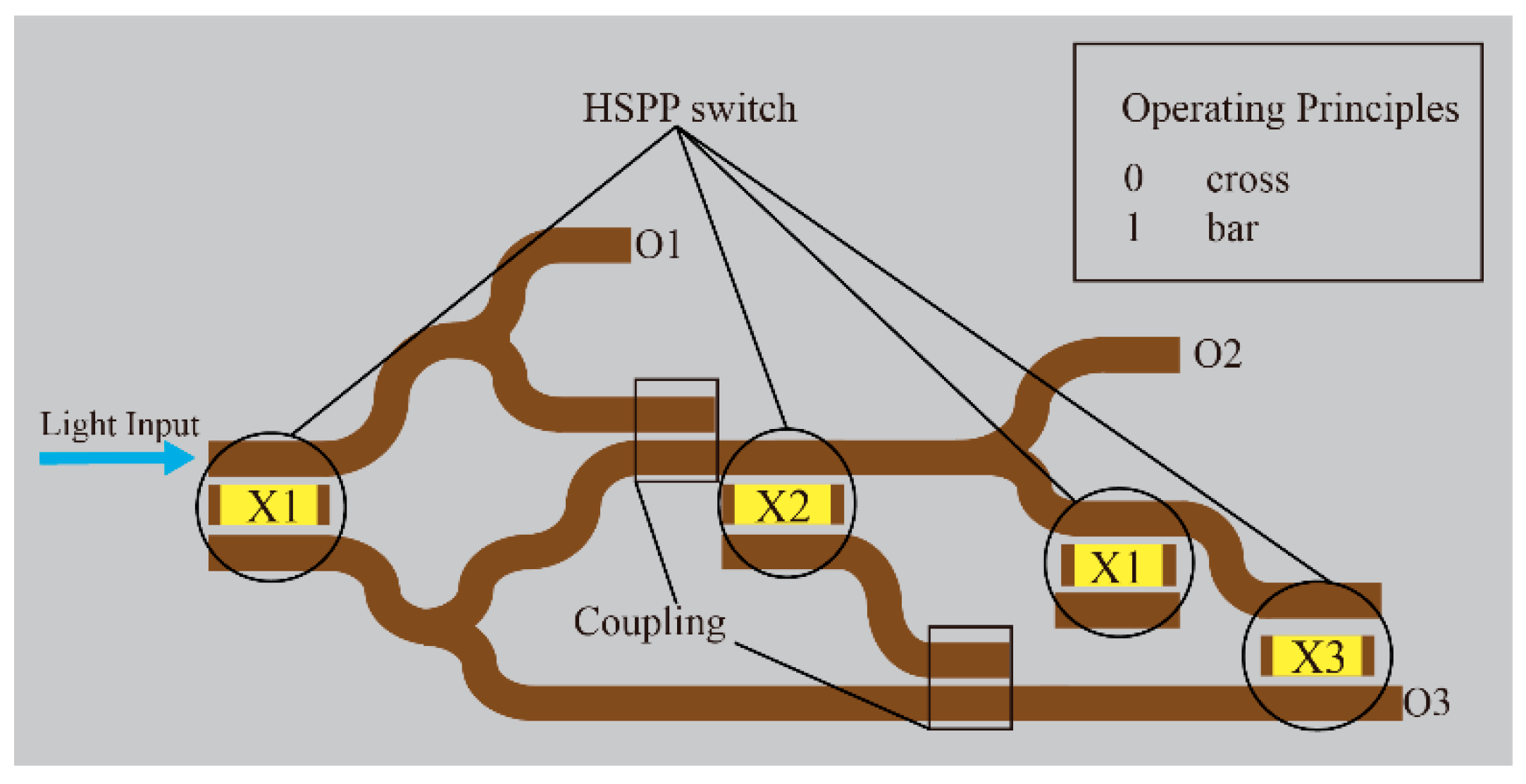
We designed a Hybrid electro-optic Toffoli logic structure based on an HSPP switch, as shown in Figure 2. The Hybrid electro-optic Toffoli logic structure is equipped with an optical signal input port, Light Input, three electrical signal control interfaces designated as X1, X2, and X3, respectively, and three optical signal output ports designated as O1, O2, and O3, respectively. The structure includes four HSPP switches, two dual waveguide couplers, and three Y-shaped splitters. The HSPP switches between cross and bar states under 0 and 1 logical electrical signals. The coupler is responsible for completing the coupling of optical signals in the optical path. Of course, a Y-shaped optical path coupler can also be used for design, but we found that waveguide coupling efficiency is higher. Therefore, in this design, we adopted a waveguide coupler based on coupling mode theory. The Y-shaped splitter is responsible for splitting the optical signal input from the front-end into two.
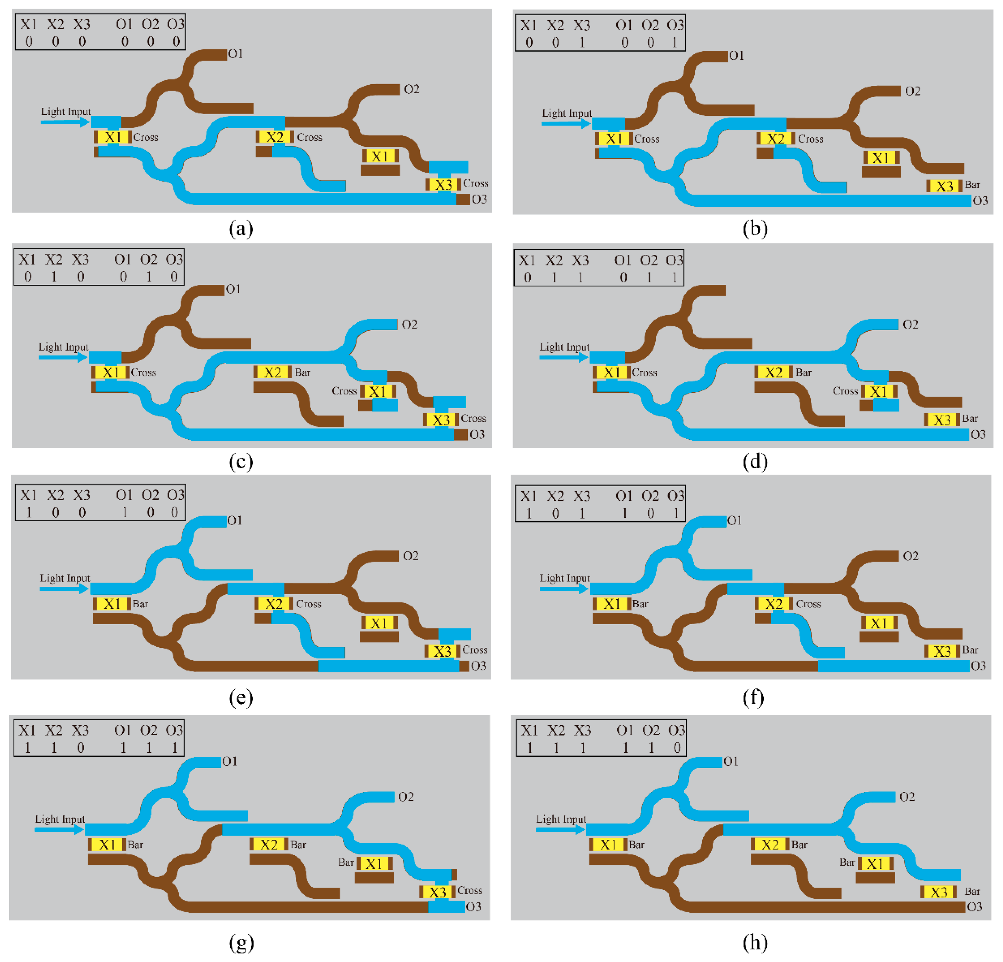
As shown in Figure 3, Figure 3a–h represents the optical signal transmission paths for each state under the input conditions of 000 to 111, respectively. For example, in Figure 3a, when the input signal is 000, the working state of each HSPP switch is crossed, and the optical signal switches from the upper end of X1 to another waveguide. The Y-shaped splitter divides the optical signal into two paths. When the upper optical signal is transmitted to X2, it is cross-switched to another waveguide and finally coupled to X3 in the second waveguide coupler. X3 is in a cross-state, so the outputs of O1, O2, and O3 are 000 in sequence. The implementation of logical functions for other states is shown in Figure 3b–h, respectively.

4. Simulation and Performance Analysis

In the hybrid electro-optic Toffoli logic structure, the HSPP switch, the waveguide coupler, and the Y-shaped splitter are momentous components, and the following will simulate and analyze the performance of the three key components. When simulating the device, all the optical modes used are low-order TM modes.
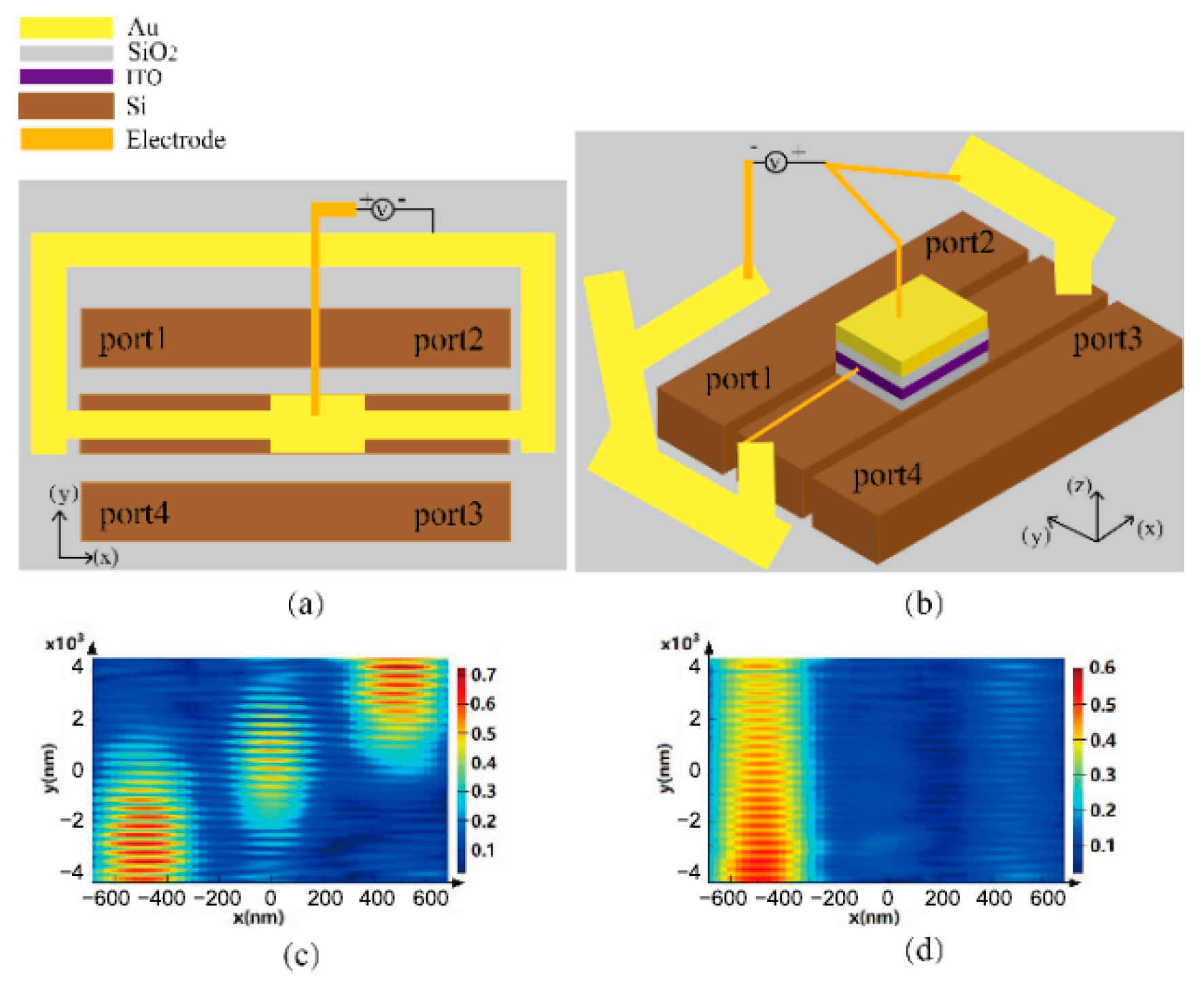
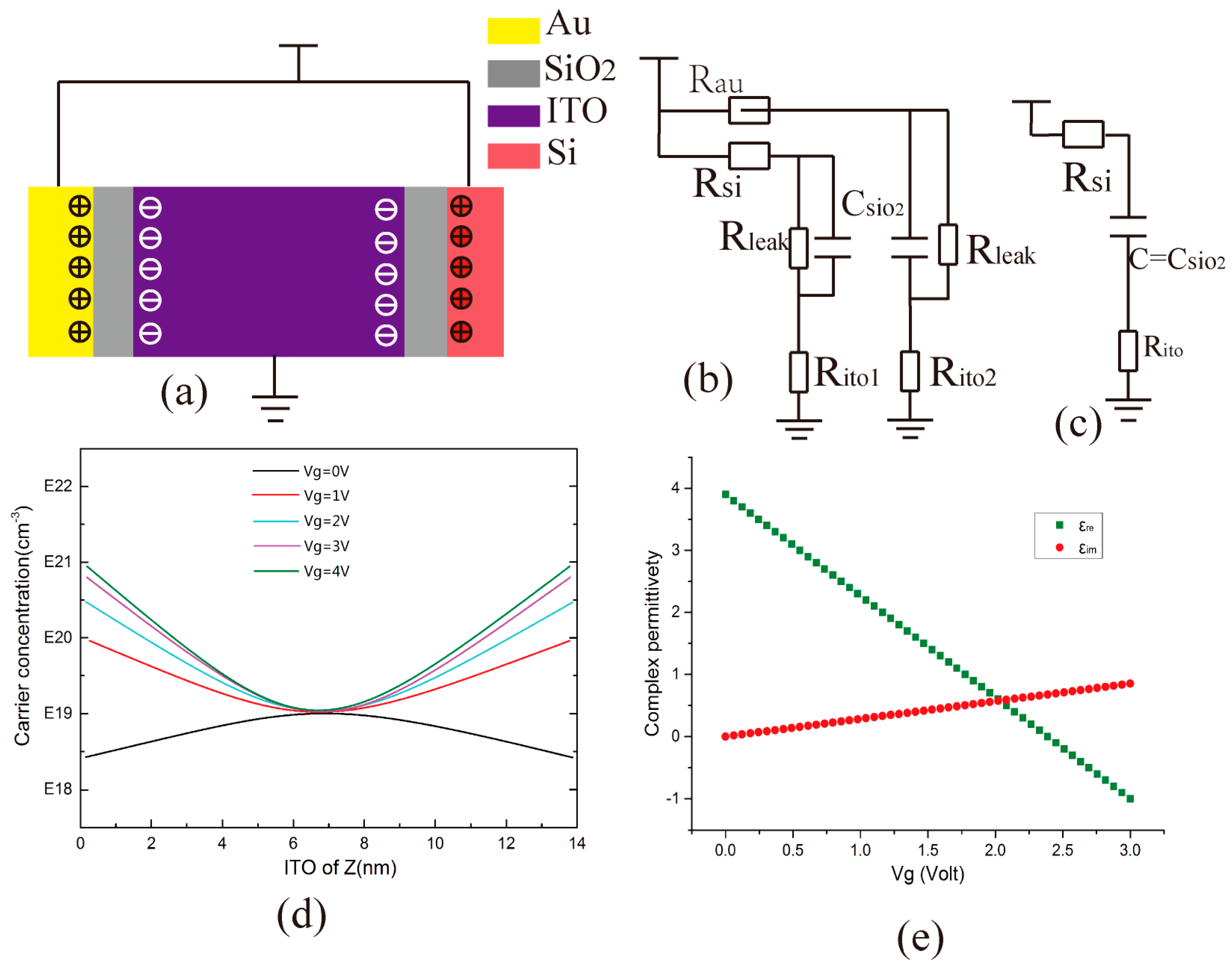
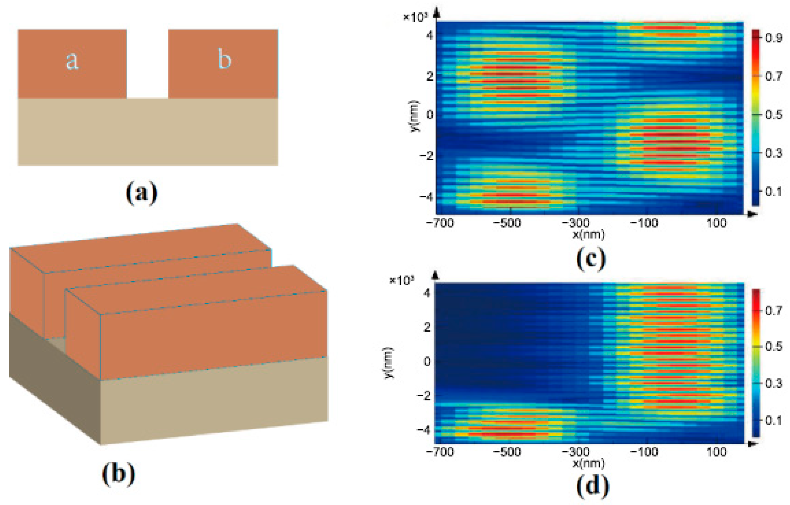
The structural design of the HSPP switch model is shown in Figure 4b. There are three silicon waveguides, a, b, and c, on the SiO2, respectively. The a and b silicon waveguides have Indium Tin Oxide (ITO)-activated film interlayers, and the top is deposited with Au metal electrode [22,23,24]. The top Au and waveguide are defined as positive electrodes, and the middle ITO film is defined as a negative electrode [25]. From the silicon waveguide to the top Au electrode, it can be seen as a Metal Oxide Semiconductor (MOS) structure device, as shown in Figure 5a. It has a similar field effect to MOS. When an external voltage is applied, the interface between the transparent conducting oxides (TCOs) material layer and the dielectric layer can quickly form carrier accumulation. The concentration of charge carriers in the accumulation or depletion region can be controlled by applying a bias voltage, thereby achieving a change in the dielectric constant (refractive index) of TCOs. When the real part of the dielectric constant of the TCO material layer approaches zero, it is defined as the dielectric constant Epsilon Near Zero (ENZ). When the dielectric constant approaches zero, it greatly enhances the overlap integration between the electromagnetic field and the electro-optic material layer, effectively improving the electromagnetic wave absorption efficiency [26]. Therefore, most TCO-based control devices usually adopt this structure to construct MOS capacitor structures, and obtain the TCO material dielectric constant ENZ state by applying an appropriate voltage, thereby achieving electrical absorption modulation. Its dielectric constant conforms to the Drude model [27]:
ε = ε N I T O q 2 ( ω 2 + i ω γ ) ε 0 m
where the ε is the high-frequency dielectric constant ( ε = 3.9 ); N I T O is the electron concentration of the ITO material; ω is the angular frequency; γ is the carrier scattering rate ( γ = 1.8 × 10¹⁴ rad/s); m is the effective mass of charge carriers ( m = 0.35 m 0 , m 0 is electronic mass, m 0 = 9.31 × 10 31 kg); q is the charge of an electron ( q = 1.6 × 10 19   C ); ε 0 is the vacuum dielectric constant ( ε 0 = 8.85 × 10⁻¹² F/m).
We calculated the variation in ITO carrier concentration with the voltage applied to it, according to the reference [24,28], and used the following simple model for calculation:
N I T O = N 0 + ε 0 · κ S i O 2 · V g q · H S i O 2 · H a c c
According to the reference [29], where N 0 = 1 × 10 19   c m 3 , it is the carrier concentration of the ITO. H S i O 2 is the thickness of the insulating layer SiO2 in the model structure, and H a c c is the thickness of free charge carriers accumulated beneath the ITO surface by SiO2. According to [22,30], H a c c = 7   nm ; this thickness can also be obtained from the simulation study below. We used Lumerical’s device software to simulate and solve the changes in ITO carrier concentration under applied voltage. The applied voltage ranged from 0 V to 4 V with a step size of 0.01 V. The changes in carrier concentration are shown in Figure 5d, while the complex dielectric constant varies with voltage, as shown in Figure 5e. When the voltage is 2.35 V, the carrier concentration of the ITO-activated material film is 6.57 × 1020 cm−3; the real part of its composite dielectric constant is close to zero; the imaginary part is 0.671, and the corresponding refractive index is 0.54 + i0.43. When the voltage is 0 V, the carrier concentration of the ITO-activated material film is 0.967 × 1019 cm−3; the imaginary part of its composite dielectric constant is close to zero; the real part is 3.9, and the corresponding refractive index is 1.98 + i0.36. In the FDTD software 2020 R2 simulation, the refractive index of the ITO material was simulated using the above refractive index.
The transmission rate is a key parameter indicator for measuring the performance of logic devices [23]. The voltage control method in Figure 5a can be equivalent to the circuit shown in Figure 5b and can be simplified to the simplified circuit shown in Figure 5c. According to reference [31], the transmission rate of the half adder designed in this paper can be calculated according to the MOS structure junction transmission rate, expressed by the following formula:
f m a x = 1 2 π R C
In the above equation, according to the definition of a capacitor, C can be expressed as
C = ε 0 ε S d
where ε 0 = 8.85 × 10 12   F / m ; d is the thin of the S i O 2 ; S is the capacitance junction area; S = L m o d u l a t e W i g , and the W i g is the waveguide width. The width of the ITO film is consistent with the width of the waveguide. R is the series connection of the equivalent resistance of silicon and the ITO semiconductors. According to [31], the equivalent resistance of the silicon electrode is assumed to be 500 Ω. In addition, the equivalent resistance of the ITO-activated material thin films can be expressed as
R I T O = L σ S
where L is half the thickness of the ITO film; L = 1 2 H I T O ; S is the cross-sectional area of the ITO film perpendicular to the Z-direction of the device; S = L m o d u l a t e W g ; σ is the conductivity of the ITO-activated material thin film; σ = n q μ n . According to reference [32], the carrier mobility of the ITO thin film is μ n =   20 c m 2 / V · s ; n is the carrier concentration of the ITO-activated material thin film. In this design, n is set as the carrier concentration when the voltage is 0 V, with a value of 0.967 × 1019 cm−3. In fact, when a certain voltage is applied to the doped semiconductor, the carrier concentration will be greater than the initial concentration [22]. Therefore, the equivalent resistance of the activated material thin film is lower than the theoretical calculation value.
According to reference [31], the power consumption required for transmitting 1 bit can be calculated based on the energy consumption of capacitor charging (energy consumption is not required for discharging), which can be expressed as
E = 1 2 C V 2
where the parameters of SiO2 thickness and the ITO film thickness mentioned above were optimized using the parameters from reference [32], and after calculation, R I T O = 30.95   Ω ; adding an equivalent resistance of 500 Ω for the silicon electrode gives R = 530.95 Ω . Meanwhile, according to Formula (5), the capacitance can be calculated as C = 4.867 × 10 15 F. According to Formula (4), by calculation, the operating speed of the device is obtained as f m a x = 61.62   GHz . According to Formula (7), by calculation, E = 13.439 × 10 15   J . So, the power consumption required to transmit 1 bit is 13.44 fJ.
According to the perturbation theory, the coupling system can be used as an ideal waveguide for some kind of perturbation. The wave equation for a dielectric optical waveguide can be used [30] as follows:
2 E ( r , t ) = μ 0 ε 0 2 E ( r , t ) t 2 + μ 0 2 t 2 P ( r , t )
Under the effect of perturbation, the polarization intensity P(r,t) of the medium in the waveguide undergoes a perturbation variation, which can be expressed as
P ( r , t ) = P 0 ( r , t ) + P p e r t ( r , t )
where P0(r,t) represents the polarization intensity of the medium in the waveguide when there is no disturbance, and Ppert(r,t) represents the additional polarization intensity caused by various disturbances related to the coupled wave. According to Equations (8) and (9), the expressions of the Ex, Ey, and Ez field components can be derived as follows:
2 E x μ 0 ε ( r ) 2 E x t 2 = μ 0 2 t 2 [ P p e r t ( r , t ) ] x
2 E y μ 0 ε ( r ) 2 E y t 2 = μ 0 2 t 2 [ P p e r t ( r , t ) ] y
2 E z μ 0 ε ( r ) 2 E z t 2 = μ 0 2 t 2 [ P p e r t ( r , t ) ] z
The optical field in a perturbed waveguide is expanded into a linear superposition of all possible modes of electromagnetic fields in the waveguide, and then, Equation (11) and the orthogonality between the wave fields of each mode are used to produce a “gradual change” in the wave field amplitude caused by the mode coupling. Under this condition,
| d 2 A m d z 2 | < < β m | d A m d z |
After analysis and derivation, we can obtain [30]:
d A s ( ) d z exp [ j ( ω t + β s z ) ] d A s ( + ) d z exp [ j ( ω t + β s z ) ] c . c = j 2 ω 2 t 2 [ P p e r t ( r , t ) ] y E y s ( x ) d x
The left two terms in the above formula represent a wave A S ( )   propagating in the −z direction and a wave A S ( + ) propagating in the +z direction. A S ( ) and A S ( + ) are the amplitude functions of the S-th order mode wave in two directions, respectively.
The designed electro-optic modulation structure can be regarded as two waveguides, a and b, which are close to each other, as shown in Figure 6a, and the refractive indices of the two waveguides are na and nb, respectively. When the distance between the two waveguides is long enough, no coupling occurs. The wave fields are E y a ( x ) and E y b ( x ) , and their respective propagation constants are βa and βb. When the two waveguides are close enough, a coupling phenomenon occurs, and the optical field can be approximately expressed as the sum of the two light fields without disturbance, that is,
E y = A ( z ) E y ( a ) ( x ) exp [ j β a z ] + B ( z ) E y ( b ) ( x ) exp [ j β b z ]
According to Equations (1) and (2), the perturbation polarization intensity Ppert(r,t) can be obtained as:
P p e r t = ε 0 [ E y ( a ) A ( z ) ( n 2 ( x ) n a 2 ( x ) ) exp ( j β a z ) + E y ( b ) A ( z ) ( n 2 ( x ) n b 2 ( x ) ) exp ( j β b z ) ]
where n(x) is the refractive index distribution function of the coupled waveguide. By substituting this into Equation (7), we obtain the coupling equations:
d A d z = j K a b B exp [ j ( β b β a ) z ] j M a A
d B d z = j K b a A exp [ j ( β a β b ) z ] j M b B
The coupling coefficient in the formula is
K b a . a b = ω ε 0 4 [ n 2 ( x ) n a , b 2 ( x ) ] E y ( a ) E y ( b ) d x
M in Equations (10) and (11) represents a coupled waveguide, and the wave transmission coefficients relative to the uncoupled waveguides βa and βb will change to βa + Ma and βb + Mb, respectively; therefore,
M a b = ω ε 0 4 [ n 2 ( x ) n a , b 2 ( x ) ] [ E y ( a , b ) ] 2 d x
The difference between the transmission constants of the waveguide modes of the a and b waveguides is
2 δ = ( β b + M b ) ( β a + M a )
In the above formula, δ is called a phase mismatch factor. The wave energy transfer caused by mode coupling can occur only when a close match occurs, that is, when δ = 0.
Assume that only waveguide ‘a’ has single-mode optical propagation at z = 0 and that the perturbation occurs in the area where z > 0, that is
B ( 0 ) = B 0 ,   A ( 0 ) = A 0
The energies of the optical waves in waveguides a and b are respectively represented by Pa = |A(z)|2 and Pb = |B(z)|2. According to the principle of energy conservation, the following can be obtained:
d d z ( | A ( z ) | 2 + | B ( z ) | 2 ) = 0
When the waveguides a and b have the same size and refractive index structure and their material parameters are the same, the coupling coefficient is
K b a = K a b ,   M a b = M b a
According to the above conditions, the solution to the coupling Equation (10) is
A ( z ) = B 0 Κ ( Κ 2 + δ 2 ) 1 2 exp ( j δ z ) sin [ ( Κ 2 + δ 2 ) 1 2 z ]
B ( z ) = B 0 exp ( j δ z ) { cos [ ( Κ 2 + δ 2 ) 1 2 z ] j δ ( Κ 2 + δ 2 ) 1 2 sin [ ( Κ 2 + δ 2 ) 1 2 z ] }
where K2 = |Kab|2. The energy carried in waveguides a and b is expressed as
P a ( z ) = P 0 K 2 K 2 + δ 2 sin 2 [ ( K 2 + δ 2 ) 1 2 z ]
P b ( z ) = P 0 P a ( z )
In the above formulas, P0 = |A(0)|2 is the input energy of waveguide ‘a’. In phase matching, that is, when the propagation constants of the two waveguides are equal, the transmission distance is L = π/2K [30]. As shown in Figure 6c,d, the energy is completely transferred from waveguide ‘a’ to waveguide ‘b’.
To reduce coupling losses, according to the coupling distance formula L = π/2K, the coupling distance can be set to Lcoupling = /2K. To reduce the loss caused by multiperiod coupling, we set n to 1. For this purpose, we conducted simulation studies on the coupling distance of waveguides, setting the gap between waveguides between 28 nm and 68 nm. Set the step value to 5 nm. From the experimental results in Figure 7, it can be seen that when the gap is between 35 and 40 nm, the loss is small. Therefore, it is recommended to set the gap to 38 nm. The insertion loss of the coupler can be calculated using the insertion loss formula.
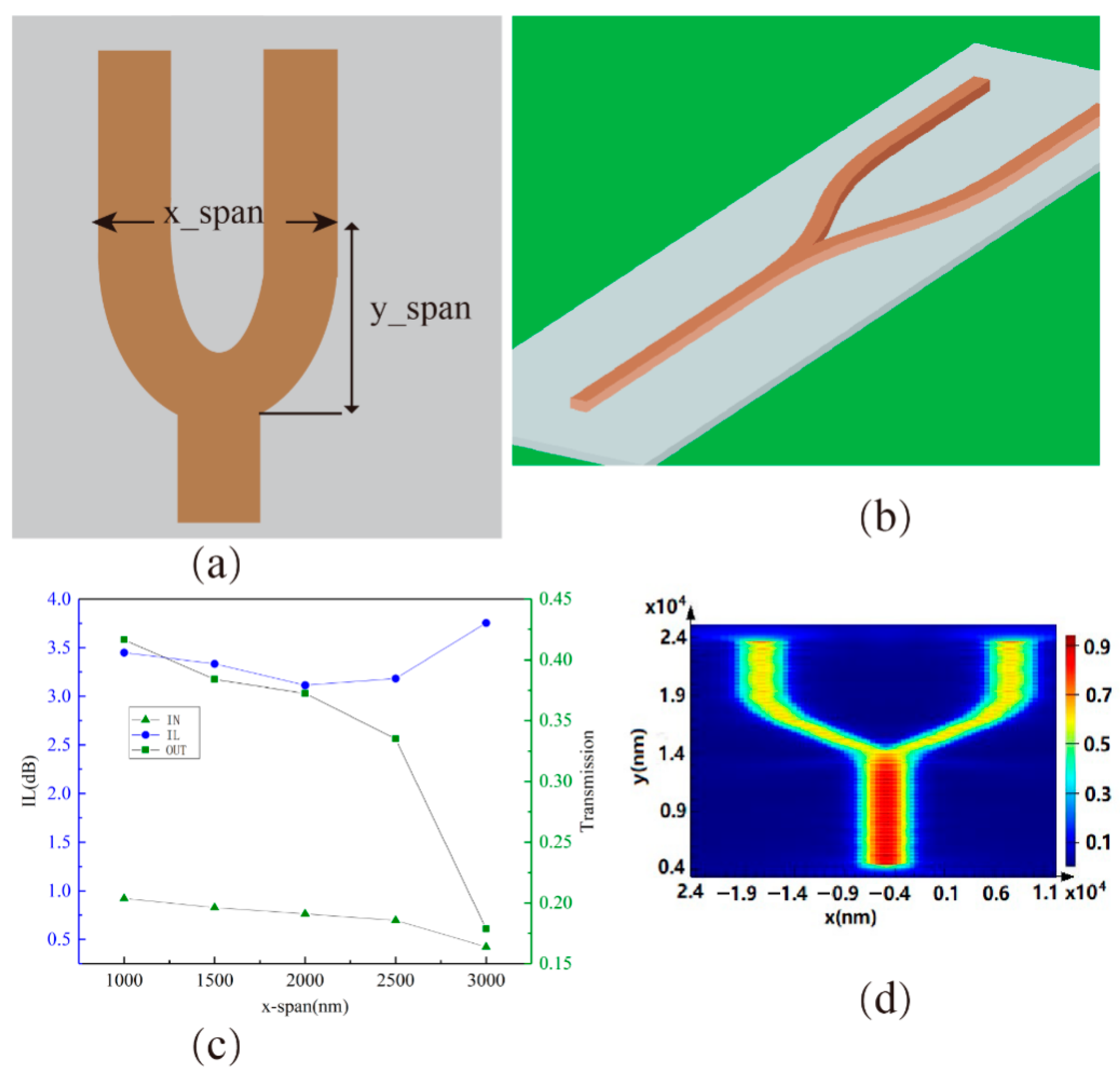
There are three Y-shaped splitters in the Toffoli electro-optic hybrid logic structure, and their performance mainly affects the insertion loss of the entire Toffoli electro-optic hybrid logic. The structure of the Y-shaped splitter is shown in Figure 8a. We fixed its y-span parameter at 4000 nm and then studied the insertion loss of the Y-shaped splitter by changing the x-span from 1000 nm to 3000 nm. From the simulation results in Figure 8c, it can be seen when the x-span is 2000 nm, and the insertion loss is small, that is, when the x-span size is half of the y-span size, the insertion loss is small, and the insertion loss is 3.11 dB.
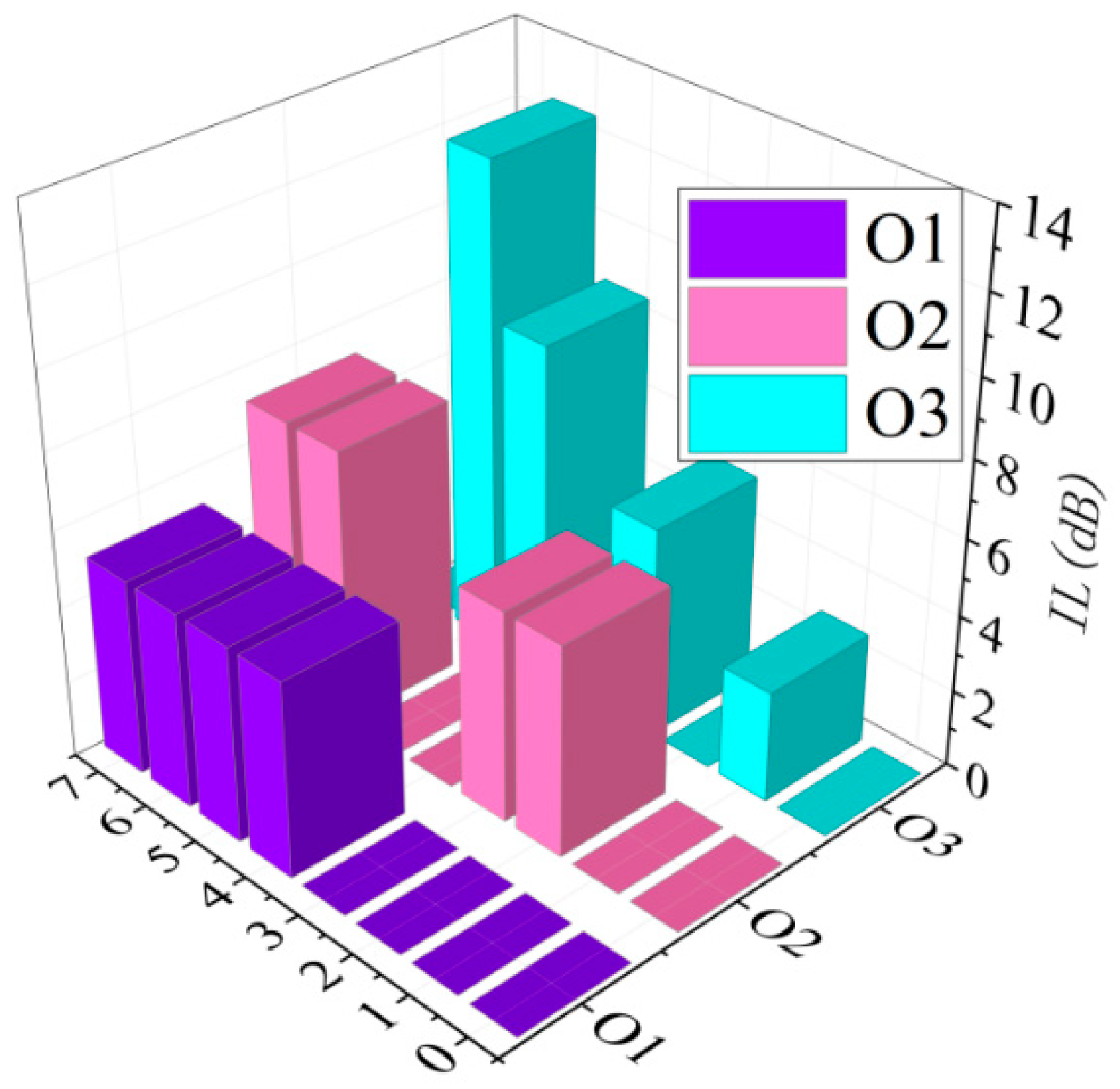
We conducted experimental simulations on the insertion loss of the entire Toffoli electro-optic hybrid logic by connecting the transmission properties of each element. Using the parameters from reference [32], the insertion losses of the bar and cross states of the HSPP switch were set to 2.1 and 0.4, respectively. The Y-shaped splitter was set to 3.11, and the insertion loss of the waveguide coupler was set to 1.13. After simulating the experiment and plotting the results in Figure 9, we found that the highest insertion loss was the O3 output in the 110 state, with an insertion loss of 12.93 dB. The main reason was that the optical path passed through three bar states of HSPP switches and two Y-shaped splitters in the 110 state. The insertion loss of the bar state of HSPP switches was 2.1 dB, while the insertion loss of Y-shaped splitters exceeded 3 dB. The average loss of each state output is 6.4 dB.
We conducted simulation studies on the extinction ratios of various output ports of O1, O2, and O3, using the formula referenced in [23]:
E R = 10 log P o f f P o n
In the above equation, for output port O1, P_on represents the optical power output of 1 in the 100-111 state when there is an optical signal output, and P_off represents the optical power output of 0 in the 000-011 state when there is no optical signal output. For output port O2, the corresponding 010, 011, 110, and 111 states output 1 when there is an optical signal output, and the corresponding 000, 001, 100, and 101 states output 0 when there is no optical signal output. For output port O3, when there is an optical signal output, the corresponding states 001, 011, 101, and 110 output 1, and when there is no optical signal output, the corresponding states 000, 010, 100, and 111 output 0.
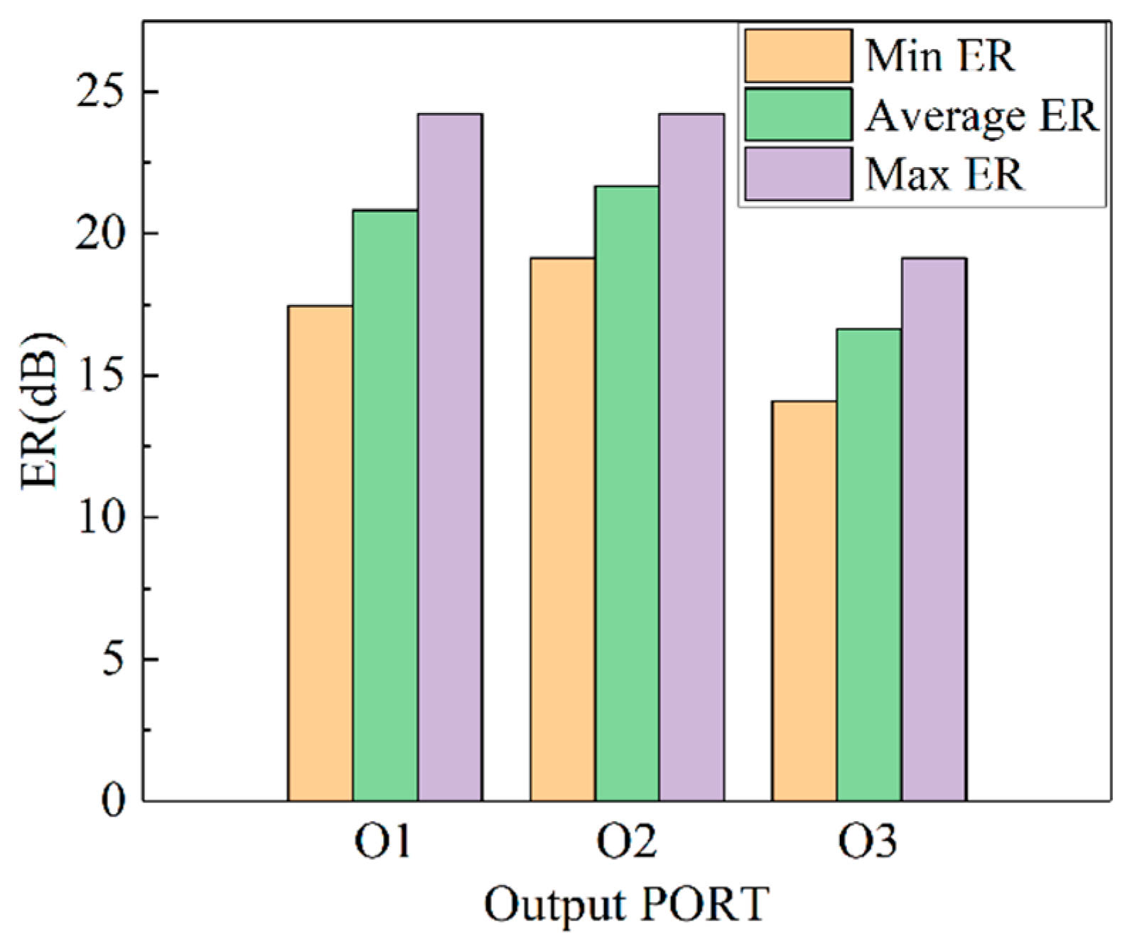
From the simulation experiment, showed in the Figure 10, it can be seen that the extinction ratio of output port O3 is relatively small, at 14.1 dB, and the highest extinction is at output port O2. The average extinction ratio of each output port of O1, O2, and O3 is 19.7 dB.

5. Discussion

We studied the designed electro-optic hybrid Toffoli logic and found through simulation experiments that the operating frequency of the device can be as high as 61.62 GHz, with an average insertion loss of 6.4 dB. The power consumption required to transmit 1 bit is 13.44 fJ. The average extinction ratio of each output port of O1, O2, and O3 is 19.7 dB. We found that the highest insertion loss is the O3 output in the 110 state, with an insertion loss of 12.93 dB. The main reason is that the optical path passes through three bar states of HSPP switches and two Y-shaped splitters in the 110 state. The insertion loss of the bar state of HSPP switches is 2.1 dB, while the insertion loss of Y-shaped splitters exceeds 3 dB. To solve this problem, we need to change the strategy to reduce the use of bar states and Y-shaped splitters to transmit optical signals, which can reduce the global average insertion loss.
In the literature [22], there are many extensive explorations and developments in integrated photonics for various material systems, such as silicon (Si), silicon nitride (SiN), lithium niobate (LN), III–V semiconductors, aluminum nitride (AlN), silicon carbide (SiC), and so on. Due to the fact that hybrid silicon-based waveguides surface plasmon polaritons are HSPP, silicon-based waveguides are added to vacuum transmission media to reduce severe Ohmic attenuation. Silicon-based photonic devices have the characteristics of being compatible with complementary metal oxide semiconductor (CMOS) processes; therefore, the proposed electro-optical hybrid digital multiplier based on HSPP technology can be fabricated using this SOI-platform-compatible CMOS technology for high-performance computing. Our research studied the working speed of the control unit and found that the junction capacitance of the control unit is 2.07 fF, which is smaller than the tens of 35 fF mentioned in the reference [22]. This is due to the application of surface plasmon excimer technology, which effectively reduces the area of the junction capacitance and the thickness of the dielectric film, thereby reducing the junction capacitance. At the same time, from our research, we show that the equivalent resistance of the contact electrode of our device is 500 Ω, which is much larger than the 24 Ω made in practice in the reference. Therefore, according to the current advanced production process, the contact resistance made in practice is smaller than the theoretical value. It is necessary to have higher requirements for the process to ensure that the control of X1, X2, and X3 in the device is synchronized; otherwise, the problem of logic gate competition will occur, resulting in logic errors.

6. Conclusions

We have designed a hybrid electro-optic Toffoli logic based on hybrid silicon-based waveguide surface plasmon polariton technology. By controlling the optical signal path switching through electrical signals, the logic output corresponding to the optical signal is represented at the output end, realizing the basic unit logic function of photonics computing. Firstly, the HSPP switch, waveguide coupler, and Y-shaped splitter that make up the logic were studied separately. Then, simulation experiments were conducted on the entire Toffoli electro-optic hybrid logic. The experimental results showed that the hybrid electro-optic Toffoli logic has the advantages of low power consumption, fast operation speed, and high extinction ratio. Currently, the problem encountered is that the optical insertion loss of the 110 state is relatively higher.

Author Contributions

Conceptualization, Z.L. and Y.Y.; methodology, Z.L.; software, Y.F.; validation, Y.S. and Z.L.; formal analysis, Z.L. and Y.F.; investigation, Z.L., Y.S. and Y.Y.; resources, Z.L.; datacuration, Y.F.; writing—original draft preparation, Z.L.; writing—review and editing, Y.Y.; visualization, Y.S.; supervision, Y.Y.; project administration, Z.L.; funding acquisition, Z.L. All authors have read and agreed to the published version of the manuscript.

Funding

This work is supported by the Guangxi Natural Science Foundation Joint Funding Project 2021GXNSFBA220023, in part, by the Hechi University High-Level Talents Research Project (No. 2022GCC010) and the Research Basic Ability Improvement Project for Young and Middle-aged Teachers of Guangxi Universities (2023KY0633), the Supported by Guangxi Key Laboratory of Automatic Detecting Technology and Instruments (YQ24210).

Institutional Review Board Statement

Not applicable.

Informed Consent Statement

Not applicable.

Data Availability Statement

All data included in this study are available upon request by contact with the corresponding author.

Conflicts of Interest

The authors declare no conflicts of interest.

References

  1. Zhou, H.; Zhao, C.; He, C.; Huang, L.; Man, T.; Wan, Y. Optical computing metasurfaces: Applications and advances. Nanophotonics 2024, 13, 419–441. [Google Scholar] [CrossRef] [PubMed]
  2. Farmakidis, N.; Dong, B.; Bhaskaran, H. Integrated photonic neuromorphic computing: Opportunities and challenges. Nat. Rev. Electr. Eng. 2024, 1, 358–373. [Google Scholar] [CrossRef]
  3. Ning, S.; Zhu, H.; Feng, C.; Gu, J.; Jiang, Z.; Ying, Z.; Midkiff, J.; Jain, S.; Hlaing, M.H.; Pan, D.Z.; et al. Photonic-electronic integrated circuits for high-performance computing and ai accelerators. J. Light. Technol. 2024, 42, 7834–7859. [Google Scholar] [CrossRef]
  4. Anderson, J.; Kayraklioglu, E.; Reza Imani, H.; Shen, C.; Miscuglio, M.; Sorger, V.J.; El-Ghazawi, T. Virtualizing a post-moore’s law analog mesh processor: The case of a photonic pde accelerator. ACM Trans. Embed. Comput. Syst. 2023, 22, 1–26. [Google Scholar] [CrossRef]
  5. Chao, C.S.; Wu, Z.Y.; Lee, Y.K.; Huang, P.W.; Chang, S.Y.; Tsai, S.Y.; Duh, J.G. Enhancing mechanical properties via the dual effect of Ni addition and temperature gradient for 5 μm Cu/Sn-3.0 Ag-0.5 Cu/Cu transient liquid phase bonding. Mater. Sci. Eng. A 2023, 870, 144863. [Google Scholar] [CrossRef]
  6. Mohammad, A.; Das, R.; Mahjabeen, F. Synergies and Challenges: Exploring the Intersection of Embedded Systems and Computer Architecture in the Era of Smart Technologies. Asian J. Mechatron. Electr. Eng. 2023, 2, 105–120. [Google Scholar]
  7. Ji, C.; Huang, H.; Wang, T.; Huang, Q. Recent advances and future trends in processing methods and characterization technologies of aluminum foam composite structures: A review. J. Manuf. Process. 2023, 93, 116–152. [Google Scholar] [CrossRef]
  8. Cao, W.; Bu, H.; Vinet, M.; Cao, M.; Takagi, S.; Hwang, S.; Ghani, T.; Banerjee, K. The future transistors. Nature 2023, 620, 501–515. [Google Scholar] [CrossRef] [PubMed]
  9. McMahon, P.L. The physics of optical computing. Nat. Rev. Phys. 2023, 5, 717–734. [Google Scholar] [CrossRef]
  10. Sankar Rao, D.G.; Fathima, M.S.; Manjula, P.; Swarnakar, S. Design and optimization of all-optical demultiplexer using photonic crystals for optical computing applications. J. Opt. Commun. 2024, 44, s197–s202. [Google Scholar] [CrossRef]
  11. Weaver, M.J.; Duivestein, P.; Bernasconi, A.C.; Scharmer, S.; Lemang, M.; Thiel, T.C.; Hijazi, F.; Hensen, B.; Gröblacher, S.; Stockill, R. An integrated microwave-to-optics interface for scalable quantum computing. Nat. Nanotechnol. 2024, 19, 166–172. [Google Scholar] [CrossRef] [PubMed]
  12. Li, C.; Li, M.; Wang, R.; Chen, Y.; Ren, X.; Yan, L.; Li, Q.; Gong, Q.; Li, Y. Dynamically encircling exceptional points for robust eigenstate generation and all-optical logic operations in a three-dimensional photonic chip. Phys. Rev. Res. 2024, 6, 013203. [Google Scholar] [CrossRef]
  13. Chen, Y.; Shen, C.; Li, Q.; Li, J.; Deng, X. Dual-Band All-Optical Logic Gates by Coherent Absorption in an Amorphous Silicon Graphene Metasurface. Nanomaterials 2024, 14, 335. [Google Scholar] [CrossRef]
  14. Kaur, S.; Singh, M.L.; Singh, M. Performance comparison of all-optical logic gates using electro-optic effect in MZI-based waveguide switch at 1.46 µm. J. Opt. Commun. 2024, 44, s231–s243. [Google Scholar] [CrossRef]
  15. Goswami, K.; Mondal, H.; Sen, M. Design of all optical logic half adder based on holes-in-slab photonic crystal. Opt. Quantum Electron. 2024, 56, 271. [Google Scholar] [CrossRef]
  16. Kotb, A.; Zoiros, K.E.; Chen, W. All-Optical XOR, AND, OR, NOT, NOR, NAND, and XNOR Logic Operations Based on M-Shaped Silicon Waveguides at 1.55 μm. Micromachines 2024, 15, 392. [Google Scholar] [CrossRef] [PubMed]
  17. Hassangholizadeh-Kashtiban, M.; Alipour-Banaei, H.; Tavakoli, M.B.; Sabbaghi-Nadooshan, R. Creation of a fast optical Toffoli gate based on photonic crystal nonlinear ring resonators. J. Comput. Electron. 2020, 19, 1281–1287. [Google Scholar] [CrossRef]
  18. Liu, Z.; Yang, X.; Han, W.; Yan, R.; Yan, T.; Wang, P. Design of an optical Toffoli gate for reversible logic operation using silicon photonic integrated circuits. In Proceedings of the Seventh Symposium on Novel Photoelectronic Detection Technology and Applications, Kunming, China, 5–7 November 2020; Volume 11763, pp. 985–997. [Google Scholar]
  19. Yu, R.L.; Li, J.; Chen, W.W.; Wang, P.J. Silicon-Based All-0ptical Fredkin Gate UsingCross-Phase Modulation Effect. Acta Opt. Sin. 2021, 41, 143–151. [Google Scholar]
  20. Li, M.; Li, C.; Chen, Y.; Feng, L.T.; Yan, L.; Zhang, Q.; Bao, J.; Liu, B.H.; Ren, X.F.; Wang, J.; et al. On-chip path encoded photonic quantum Toffoli gate. Photonics Res. 2022, 10, 1533–1542. [Google Scholar] [CrossRef]
  21. Wu, Q.; Qian, J.; Wang, Y.; Xing, L.; Wei, Z.; Gao, X.; Li, Y.; Liu, Z.; Liu, H.; Shu, H.; et al. Waveguide-integrated twisted bilayer graphene photodetectors. Nat. Commun. 2024, 15, 3688. [Google Scholar] [CrossRef]
  22. Bulgakov, E.N.; Maksimov, D.N.; Ershov, A.E. Optical coupled-mode theory for dielectric solids of revolution. Phys. Rev. A 2023, 107, 043506. [Google Scholar] [CrossRef]
  23. Chen, C.; Chen, Y.; Fang, Z.; Ge, R.; Wu, J.; Chen, X. Hybrid material integration for active photonic applications. APL Photonics 2024, 9, 030903. [Google Scholar] [CrossRef]
  24. Liang, Z.; Shi, Y.; Wu, Q.; Yi, Y.; Fan, Y.; Tang, P. An electro-optic half subtractor from a silicon-based hybrid surface plasmon polariton waveguide. Open Phys. 2024, 22, 20240045. [Google Scholar] [CrossRef]
  25. Li, W.; Cheng, S.; Yi, Z.; Zhang, H.; Song, Q.; Hao, Z.; Sun, T.; Wu, P.; Zeng, Q.; Raza, R. Advanced optical reinforcement materials based on three-dimensional four-way weaving structure and metasurface technology. Appl. Phys. Lett. 2025, 126, 033503. [Google Scholar] [CrossRef]
  26. Zhixun, L.; Yunying, S.; Yunfeil, Y.; Yuanyuan, F.; Lvqing, B. Electro-Optic Hybrid Logic Gate Derived from a Silicon-Based Hybrid Surface Plasmon Polariton Waveguide. J. Nanoelectron. Optoelectron. 2022, 17, 298–304. [Google Scholar] [CrossRef]
  27. Tannaz, S.; Moradkhani, M.; Taherzade, M.; Rezaei, M.H. Ultracompact, high-extinction ratio XOR, OR, and Feynman logic gates based on plasmonic metal-insulator-metal directional couplers. Appl. Opt. 2023, 62, 644–653. [Google Scholar] [CrossRef]
  28. Ai, Z.; Yang, H.; Liu, M.; Cheng, S.; Wang, J.; Tang, C.; Gao, F.; Li, B. Phase-Transition-Enabled Dual-Band Camouflage in VO2/Ag Multilayered Nanostructures. Phys. E Low-Dimens. Syst. Nanostruct. 2025, 173, 116327. [Google Scholar] [CrossRef]
  29. Liang, Z.; Shi, Y.; Yi, Y.; Wei, Z.; Tang, P. Research on Electro-Optic Hybrid Multidigit Digital Multiplier Based on Surface Plasmon Polariton Technology. Photonics 2024, 11, 785. [Google Scholar] [CrossRef]
  30. Wang, L.; Dong, Y.; Gao, S.; Chen, K.Y.; Fang, F.C.; Jin, G.Y. Research progress of perovskite materials in the field of lasers. China Opt. 2019, 12, 993–1014. [Google Scholar] [CrossRef]
  31. Kocakulah, G. Comparison of electro-optical and dielectric properties of cobalt (II) phthalocyanine doped cholesteric liquid crystals. Opt. Mater. 2023, 141, 113949. [Google Scholar] [CrossRef]
  32. Ai, Z.; Liu, H.; Cheng, S.; Zhang, H.; Yi, Z.; Zeng, Q.; Wu, P.; Zhang, J.; Tang, C.; Hao, Z. Four peak and high angle tilted insensitive surface plasmon resonance graphene absorber based on circular etching square window. J. Phys. D Appl. Phys. 2025, 58, 185305. [Google Scholar] [CrossRef]
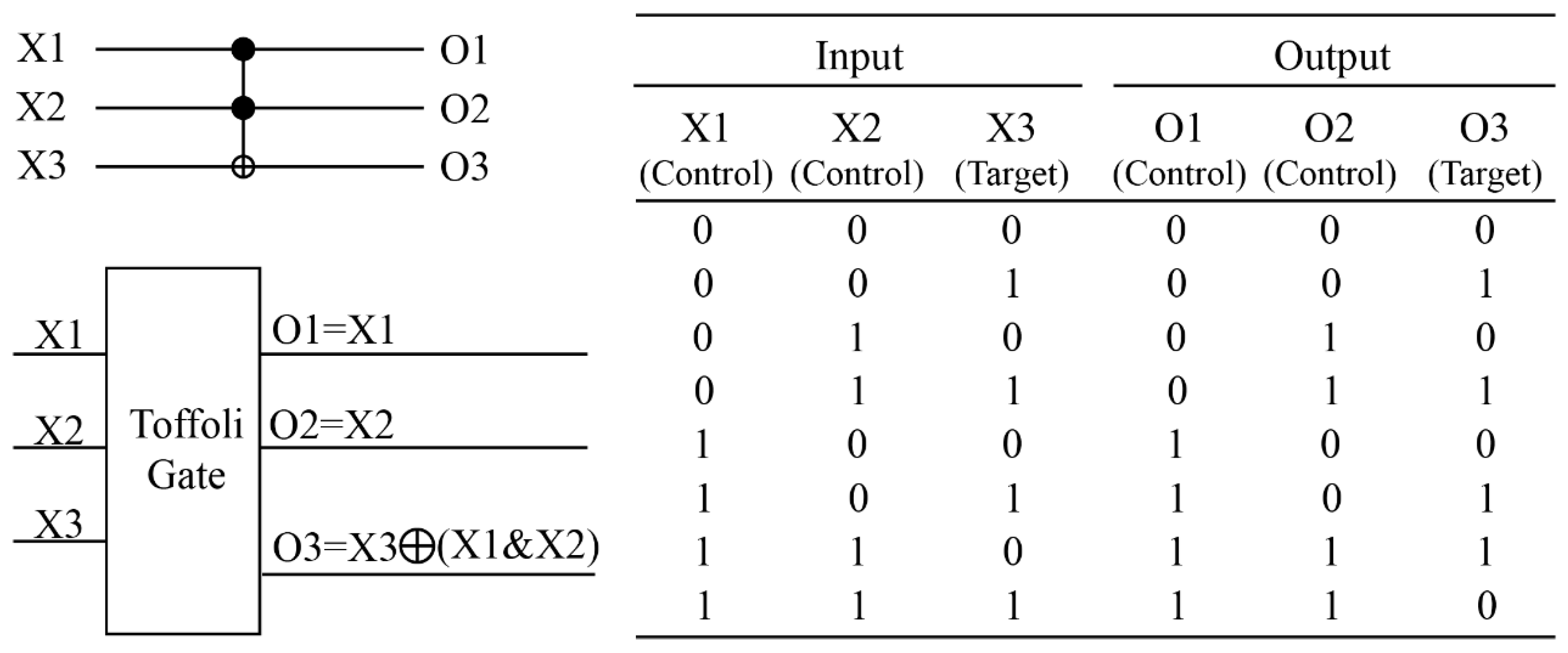
Figure 1. Basic structure of Toffoli gate.
Photonics 12 00805 g001
Figure 2. Toffoli electro-optic hybrid logic structure.
Photonics 12 00805 g002
Figure 3. Optical signal transmission paths in various states of electro-optic hybrid Toffoli logic. (a) when the input is 000, and the output is 000. (b) when the input is 001, and the output is 001. (c) when the input is 010, and the output is 010. (d) when the input is 011, and the output is 011. (e) when the input is 100, and the output is 100. (f) when the input is 101, and the output is 101. (g) when the input is 110, and the output is 111. (h) when the input is 111, and the output is 110.
Photonics 12 00805 g003
Figure 4. Logic control unit of the HSPP switch: (a) Top view of logic control unit with electrodes; (b) 3D view of logic control unit with the electrodes; (c) Electromagnetic field distribution of logic control unit without voltage applied; (d) Electromagnetic field distribution of logic control unit with voltage applied.
Photonics 12 00805 g004
Figure 5. The characteristics of ITO Films under applied voltage: (a) The model of applied voltage; (b) Equivalent circuit; (c) Simplification of Equivalent circuit; (d) The carrier concentration variation in applied voltage 0~4 V; (e) The relation between the real (green line) and imaginary (red line) components of the complex permittivity ITO under applied voltage.
Photonics 12 00805 g005
Figure 6. Dual silicon waveguide optical coupling model. (a) Side view of the dual silicon waveguide optical coupling model. (b) 3D diagram of the dual silicon waveguide optical coupling model. (c) Optical signals propagate to each other periodically between two waveguides (d) Continuous propagation of optical signal along the other silicon waveguide after single period coupling.
Photonics 12 00805 g006
Figure 7. Simulation study on gap parameters of waveguide coupling.
Photonics 12 00805 g007
Figure 8. Y-shaped splitter: (a,b) Model of Y-shaped splitter; (c) The insertion Loss of Y-shaped splitter; (d) Optical signal distribution during operation of Y-shaped splitter.
Photonics 12 00805 g008
Figure 9. Insertion loss in each state.
Photonics 12 00805 g009
Figure 10. Maximum, minimum, and average extinction ratios of each output port.
Photonics 12 00805 g010
Disclaimer/Publisher’s Note: The statements, opinions and data contained in all publications are solely those of the individual author(s) and contributor(s) and not of MDPI and/or the editor(s). MDPI and/or the editor(s) disclaim responsibility for any injury to people or property resulting from any ideas, methods, instructions or products referred to in the content.