Article

Damage Characteristics of Silicon Solar Cells Induced by Nanosecond Pulsed Laser

Department of Aerospace and Technology, Space Engineering University, Beijing 101416, China
*
Author to whom correspondence should be addressed.
Photonics 2025, 12(8), 804; https://doi.org/10.3390/photonics12080804
Submission received: 19 June 2025 / Revised: 28 July 2025 / Accepted: 9 August 2025 / Published: 11 August 2025

Abstract

The damage characteristics of monocrystalline silicon solar cells irradiated by a nanosecond pulsed laser were investigated in a vacuum environment. An 8 ns pulsed laser was used with a 1064 nm wavelength, a 2.0 J maximum pulse energy, and a millimeter-scale ablation spot diameter. The cells were irradiated by a laser with varying fluences, irradiation positions, and pulse numbers. The damage mechanism was discussed in combination with the degradation of electrical properties, the morphology of surface damage, and electroluminescence images. A single pulse mainly caused surface heating and deformation, while multi-pulse irradiation led to the formation of melting ablation craters. More severe performance degradation was caused by irradiation at the grid line site due to fracture of the grid line electrodes. Moreover, monocrystalline silicon cells showed excellent damage resistance to fixed-position irradiations at non-gridded line areas. This work reveals, for the first time in vacuum, that grid-line fracture dominates performance degradation—enabling targeted hardening for space solar cells.

1. Introduction

As renewable wireless power sources, solar cells are widely deployed in aerospace systems [1,2]. Multiple photovoltaic (PV) materials are suitable for preparing solar cells [3,4], including, but not limited to, monocrystalline silicon, polysilicon, GaAs, InP, etc. The most mature among these is the monocrystalline silicon solar cell, which stands out for its simple preparation, rich content, and higher photoelectric conversion efficiency. The 1064 nm wavelength is sometimes chosen because it is the fundamental output of space-qualified solid-state lasers, such as Nd: YAG systems, which are commonly used for orbital wireless power transmission [5]. This wavelength enables maximized energy delivery because frequency-doubling to alternative wavelengths (e.g., 532 nm) incurs substantial photon-energy losses. However, at present, the conversion efficiency of monocrystalline silicon solar cells is lower than 24%; most of the laser energy used for wireless energy transmission in space is absorbed by the surface material, leading to rapid temperature increases and potential structural damage [6,7]. Laser-induced defects can also reduce the recombination efficiency of carriers in the cells [8,9], resulting in lower conversion efficiency and unstable output voltage. As laser energy supply and processing technologies continue to be developed, it is important to study the damage characteristics of laser-irradiated silicon cells.
It is widely considered that laser-induced damage to solar cells is mainly caused by thermal melting damage [10], thermal stress deformation [11], as well as the destruction of the ordered doped structure of the cell. The damage effect depends on laser parameters such as wavelength [12,13], pulse duration [14,15], repetition frequency [16], and laser fluence [17,18]. Hiroshi et al. investigated damage efforts on InP cells by nanosecond pulsed laser irradiation [19]. They proposed a method to reflect the damaging degree of the cell by using the intensity of the probe light reflection. The results indicated that the surface damage accumulation was dependent on the doping property, with both the laser fluence and pulse number influencing the surface damage accumulation. Wang et al. irradiated monocrystalline silicon with a 1064 nm laser at millisecond, nanosecond, and picosecond pulse durations. They found that the damage threshold increased significantly with pulse width; 1 ms, 10 ns, and 10 ps pulses corresponded to thresholds of 127.2 J/cm2, 4.8 J/cm2, and 0.7 J/cm2 [15]. Hohn et al. demonstrated that the optimal wavelength of laser irradiation for GaAs cells increased with the operating temperature, leading to reduced optical losses [12]. Zhou et al. investigated electroluminescence (EL) [20], a unique phenomenon of solar cells. When an external electric field was applied, electrons and holes flowed in opposite directions and created a composite around the PN junction. Photons were then produced from these composites inside the solar cell, leading to the emission of light. The results indicated that the maximum output power of triple-junction GaAs (GaInP2/GaAs/Ge) solar cells follows a similar trend to the intensity of EL.
With regard to monocrystalline silicon solar cells, the laser-induced damage mechanism has also been investigated. In an early study, Matsuoka et al. discovered that high-power pulsed lasers cause both output power reduction and surface damage [21,22,23]. Material surface damage consists of melting, ablation craters, and cracks. In addition to thermal melting, stress shocks also play a role in damage generation. In 2018, the damage process of an Si material induced by millisecond laser ablation was investigated and experimentally combined with a numerical simulation by Jia et al. [24]. Plastic deformation occurred during the laser switch-on stage and the plastic zone was larger than the spot irradiation area. During the laser switch-off stage, more serious re-damage was induced by the solidification of the molten liquid. In 2024, Li et al. irradiated six different regions of a monocrystalline silicon cell by six laser pulses [9]. The results showed a nearly doubled output power reduction rate compared to multi-pulse irradiation at the same location. This indicates that the reduction in open-circuit voltage and short-circuit current can be attributed to changes in the values of parallel and series resistance in the cell after laser irradiation. In general, most studies on laser-induced solar cell damage have focused on material surface characteristics such as temperature distribution, melting ablation craters, thermal stress deformation, etc. However, for a laser with a wavelength of 1064 nm, its penetration depth in monocrystalline silicon is approximately 1255 µm [25], which is much larger than the thickness of the silicon cell, approximately 200 µm. Therefore, lasers with a 1064 nm wavelength may cause damage to the whole range of silicon cell thicknesses, which results in the degradation of electrical properties. At present, these internal damages have not received enough attention, especially in vacuum environments. In this study, an experimental system for the nanosecond pulsed laser ablation of monocrystalline silicon solar cells in a vacuum environment was conducted. Laser damage characteristics were analyzed through volt ampere relation (VAR), surface morphology, and the EL intensities of the cells. Further, the differences in laser irradiation on metal grid lines and non-gridded line areas were investigated at a certain repetition frequency of the laser. Finally, the damage mechanism of the nanosecond pulsed laser ablation of monocrystalline silicon solar cells was summarized. Unlike atmospheric studies [9,15,17], our vacuum experiment uncovered suppressed oxidation and accelerated grid-line failure, providing authentic space-relevant damage benchmarks.

2. Experimental Setup

The schematic diagram of the experimental system is shown in Figure 1 The whole experiment was carried out in a vacuum chamber with a vacuum degree of 10−3 Pa. A laser with λ = 1064 nm and τ = 8 ns was emitted by a Q-switch Nd: YAG laser with a maximum pulse energy of 2.0 J. The laser was focused by an optical lens and then ablated the upper surface of the monocrystalline silicon cell with a spot diameter of 1 mm, which was measured by a beam-quality analyzer. A beam splitter directed a proportion of the beam to a calibrated reference energy detector (model Ophir PD10C, Israel). The incident laser energy was calculated in real time through splitting ratios. The laser energy was controlled within ±5% via real-time energy monitoring. Each test condition was repeated 3–4 times on separate cell samples to ensure statistical reliability. The beam was re-focused before each pulse via automated XYZ stage repositioning (0.1 μm resolution) to maintain the spot position. An optical microscope (model 11XB-PC) with micrometer detection accuracy was used to detect changes in the surface morphology of the solar cells after laser irradiation. A digital source meter (model Keithley 2450) was applied to measure the real-time VAR of the cell during the damage, with electrical performance parameters, including open-circuit voltage Voc (<±1% error), short-circuit current Isc (<±1% error), and peak power Pmax (<±1% error). The maximum EL wavelength emitted by the monocrystalline silicon is near infrared, which cannot be observed by the naked eye [26]. Therefore, a DC power source, together with an EL measurement camera (model JHUM504Bs-NIR, spectral response range 400 nm–1100 nm, <±3% variation), was used to measure the relative luminescence intensity of the cell. Camera calibration was performed using an 850 nm LED standard source at 5 intensity levels (0.1–10 mW/cm2). The camera response was linearized via I EL = k × ( G raw G dark ) , where G dark is the average dark-field background (30 frames at 0.1 s exposure, 25 °C) subtracted from raw gray-scale G raw . The exposure times were optimized per fluence (0.5 s for intact cells and 2 s for damaged cells) to maintain pixel saturation < 80%. The destruction of the semiconductor material inside the solar cell can be reflected by the relative intensity of EL.
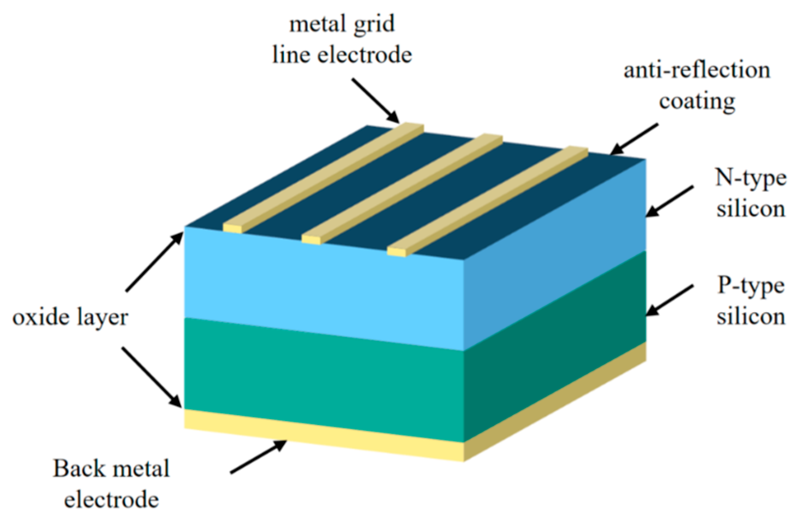
As shown in Figure 2, the structure of the monocrystalline silicon cell consists of metal grid line electrodes, anti-reflective film, silicon semiconductor material, and metal electrodes covering the bottom, in order from top to bottom. The forbidden bandwidth of silicon is between 1.1 eV and 1.3 eV, while the photon energy of sunlight is distributed between 0.8 eV and 4 eV. Therefore, the energy of most of the photons in sunlight is greater than the forbidden bandwidth of silicon materials, meeting the prerequisite of the PV effect.
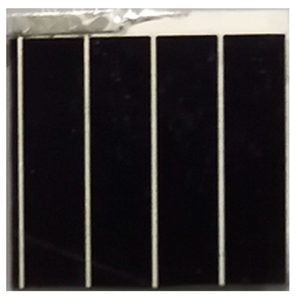
The monocrystalline cell sample (Figure 3) was selected for irradiation, measuring 1 cm × 1 cm × 200 µm with adjacent grid lines spaced ~2 mm apart. The metal grid line electrodes on the top surface and the metal electrode covering the bottom can reduce the loss of carriers in their movement within the silicon material. Since metal grid lines critically enable photogenerated carrier collection, we separately analyzed laser damage at the grid lines versus non-gridded areas. The laser irradiation rapidly heated the silicon cell surface to melting/boiling points, causing thermal damage visible in the surface images. Internal damage was assessed via EL intensity and VAR.

3. Results

3.1. Laser-Induced Damage at Non-Gridded Areas

Before placing the cell in the vacuum chamber, we wiped its surface with alcohol to prevent impurity interference with the damage effects. Laser parameters remained constant: wavelength 1064 nm, pulse duration 8 ns, and spot diameter 1 mm. Laser output power on non-gridded areas was gradually increased from 0.4 J to 1.3 J (fluence: 51.3–163.5 J/cm2). The pulse count per site was varied from 1 to 16 to analyze cumulative effects.
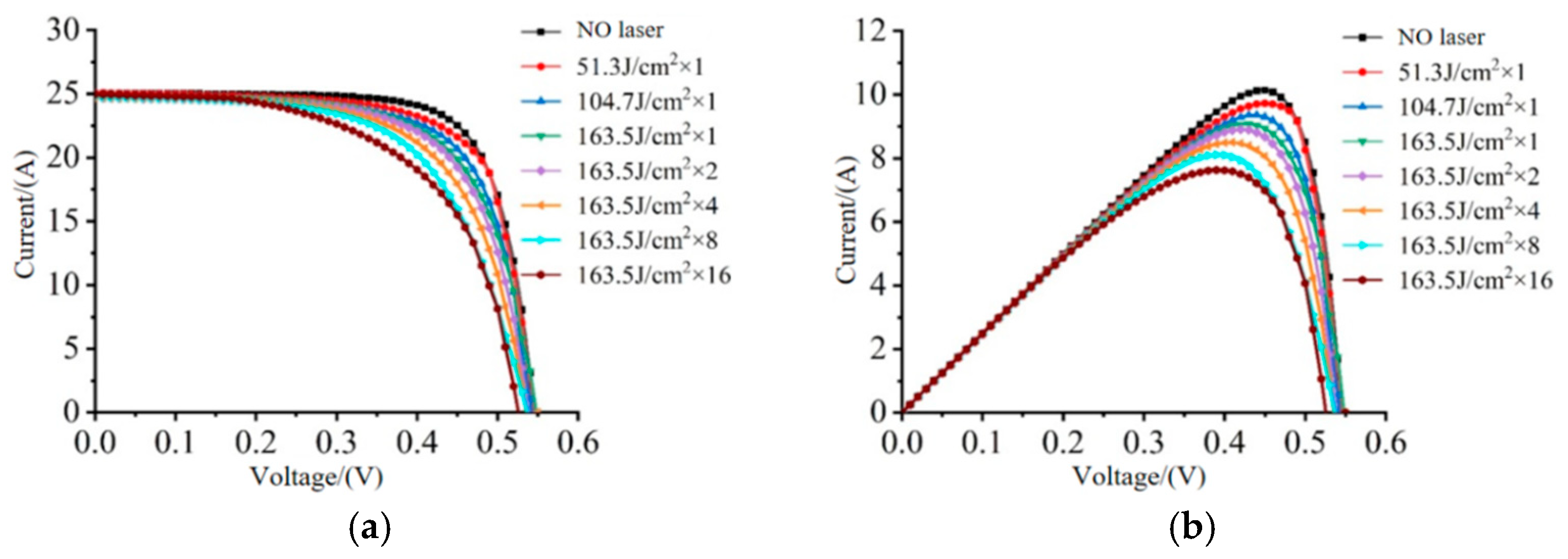
The volt–ampere and power–voltage relationship curves of the silicon cell irradiated by different laser fluences and pulse numbers are presented in Figure 4a,b, respectively. It can be seen that both the current and the output power correspond to the same voltage attenuated after laser irradiation. As the laser fluence and number of pulses increase, the peak point of the power decreases significantly, causing more severe performance degradation. Laser irradiation resulted in a weak effect on Voc and Isc, with a decrease of less than 5% through the multiple pulses irradiated. The decrease in Pmax was more significant, especially with the increase in the number of irradiation pulses. However, despite the single-pulsed laser fluence reaching 163.5 J/cm2 with sixteen pulses irradiated, the Pmax of the cell was still maintained at 75% of the original.
Figure 5 shows the damage morphology of non-gridded line areas irradiated by different laser fluences and pulse numbers. It can be seen that with single-pulsed laser irradiation, the damage area increased with the growth of the laser fluence, as shown in Figure 5a–d. The damage induced by a single-pulsed laser mainly consisted of thermal oxidation of the surface material. The bright part in Figure 5 is the oxide layer, which is called the heat-affected zone. In the process of laser pulse accumulation, massive heat accumulation caused melting spatter which formed melting ablation craters at the center of the irradiation, as shown in Figure 5f–h. The regions around the ablation craters experienced material decomposition due to thermal action, forming a heat-affected zone similar to a circular ring. When the surface of the cell was irradiated by four laser pulses of fluences at 163.5 J/cm2, melting ablation craters were observed. The area of melting ablation craters as well as the heat-affected zone both increased with the growth in the number of irradiation pulses. Eventually, the size of the melting ablation craters tended to stabilize as their area approached the laser spot. Combined with the electrical performance, it can be seen that the silicon cell can still maintain most of its output power, even if millimeter-level melting ablation craters appear on its upper surface.
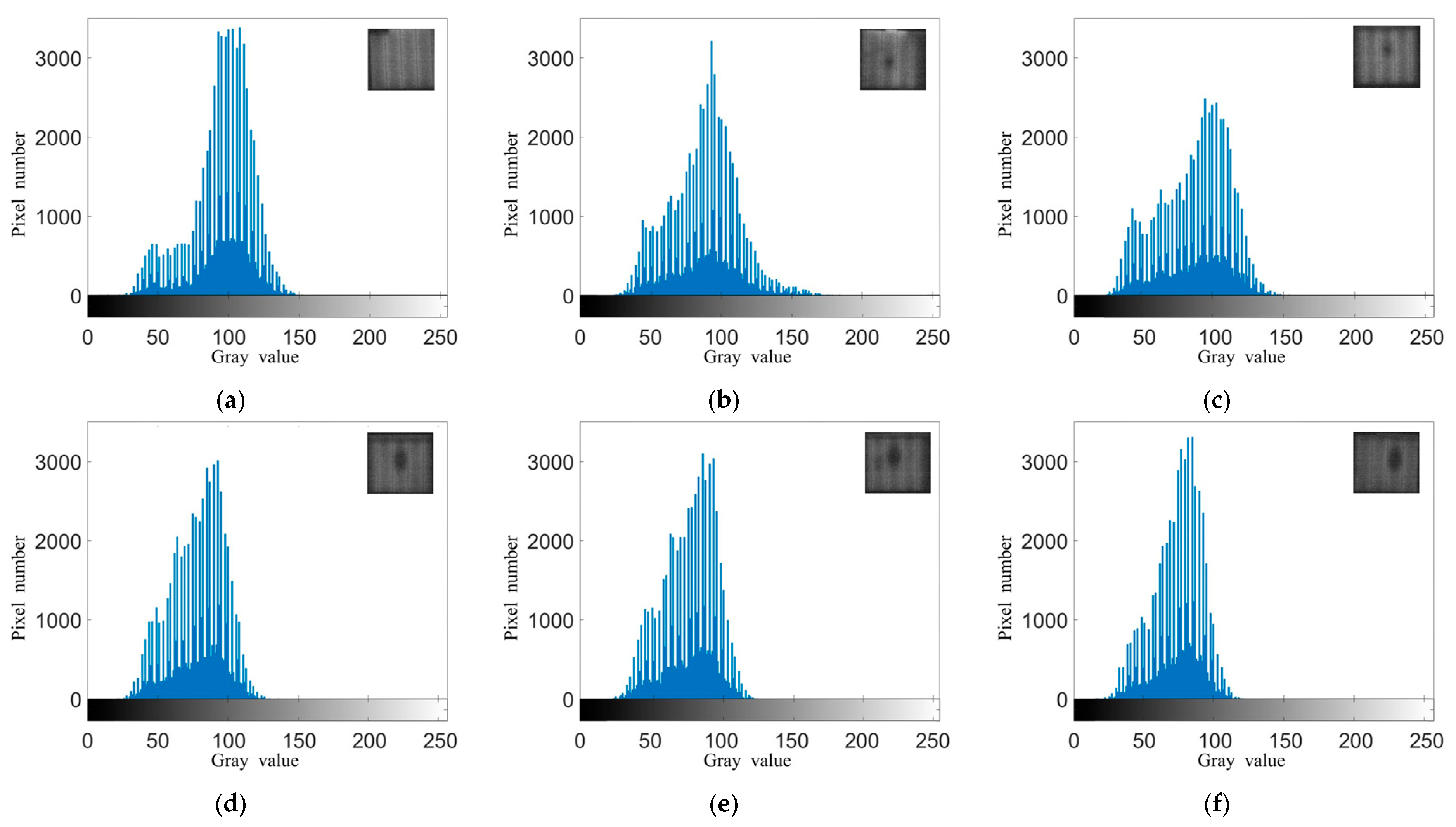
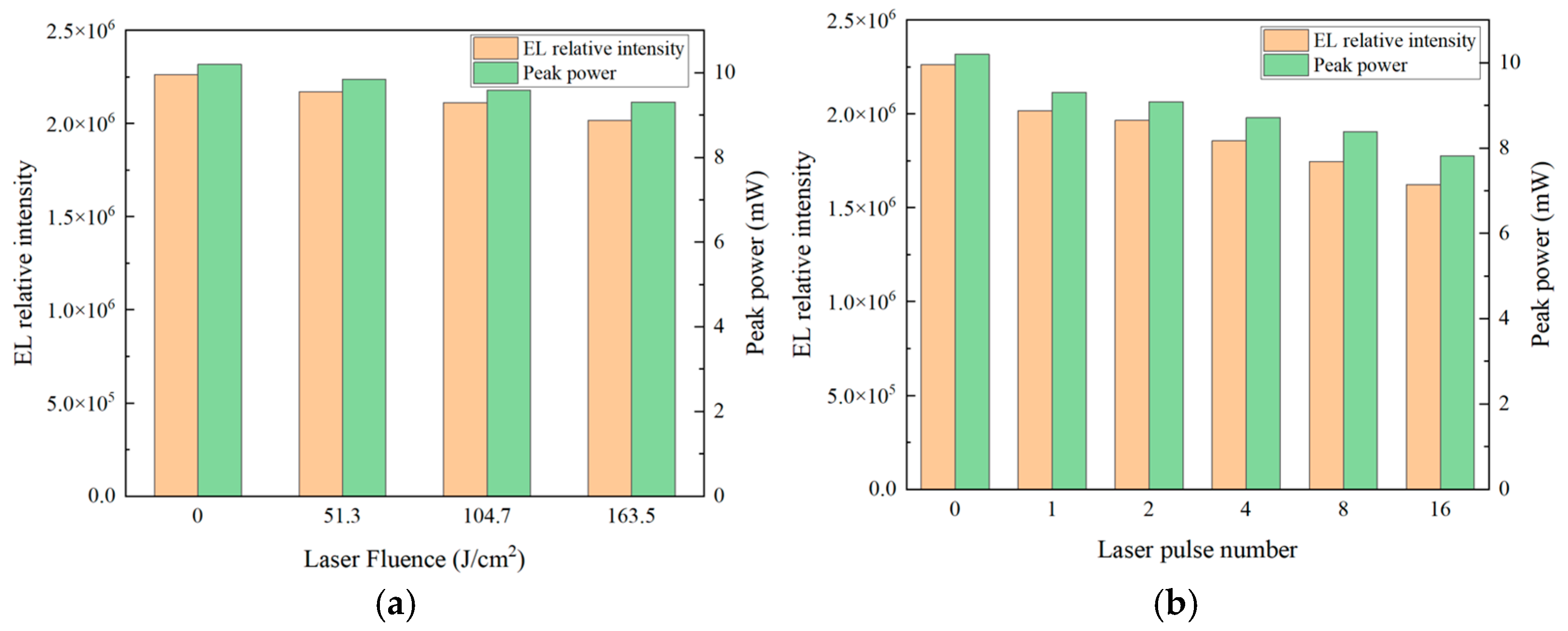
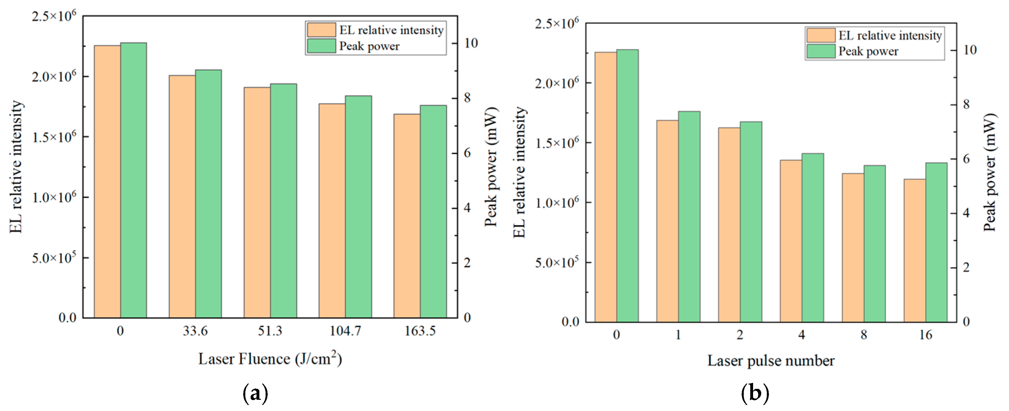
Figure 6 presents the EL images and the grey-scale alteration after the laser irradiated the silicon cell. As can be seen, the areas in which electroluminescence cannot be detected gradually increase with the growth of the laser fluence and pulse number. At lower laser fluences, damaged regions appear as small areas around the laser spot. The gray histogram shifts leftward, indicating reduced relative EL intensity. As shown in Figure 7, the electroluminescence intensity decreases with the growth of the laser fluence and pulse number. This is because damage within the cell directly leads to a degradation in the lifetime of the carriers, which reduces the electroluminescence intensity. However, similar to Pmax, the EL relative intensity of the cell is still maintained at above 80% of the original, although the pulsed laser fluence reached 163.5 J/cm2 with sixteen pulses irradiated. Therefore, it can be concluded that nanosecond laser irradiation at the non-gridded line areas of the cell only leads to a slight degradation in performance; the monocrystalline silicon cells showed satisfactory damage resistance.

3.2. Laser-Induced Damage at Metal Grid Line Electrodes

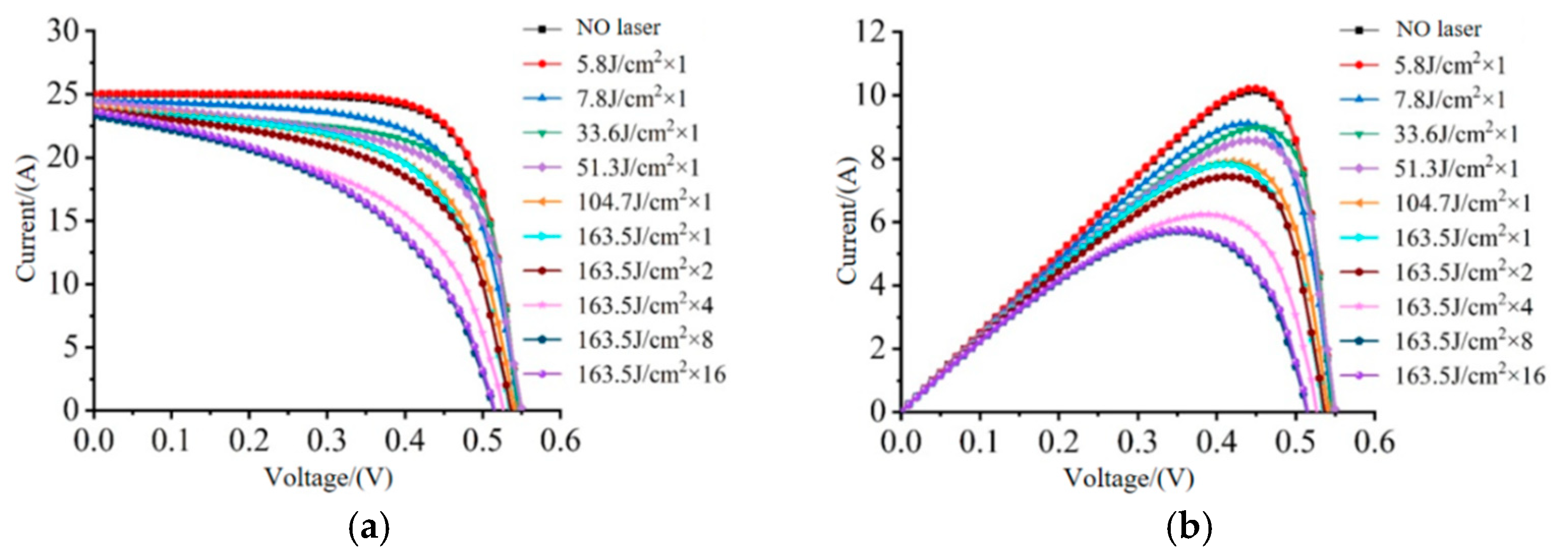
The position of the laser was adjusted to focus the irradiation spot on the metal grid line electrodes on the upper surface of the cell. The laser wavelength of 1064 nm, pulse duration of 8 ns, and irradiated spot diameter of 1 mm were still constant. The range of pulsed laser energy was adjusted to 40–1300 mJ, corresponding to a laser fluence of 5.8–163.5 J/cm2. The number of pulses irradiating at the same position was still set from 1 to 16. Figure 8a,b present the volt–ampere and power–voltage relationship after laser irradiation on the metal grid line electrodes, respectively. As the growth in laser fluence and pulse number, attenuations can be observed, which represents more severe performance degradations due to the damage. After being irradiated by sixteen laser pulses of 163.5 J/cm2, the Pmax of the cell reduced approximately 43%. Compared to irradiation on non-gridded line areas, these damages are more severe. Therefore, irradiated by lasers of the same parameters, more electrical property degradation will occur if the spot focuses on the metal grid line electrodes.
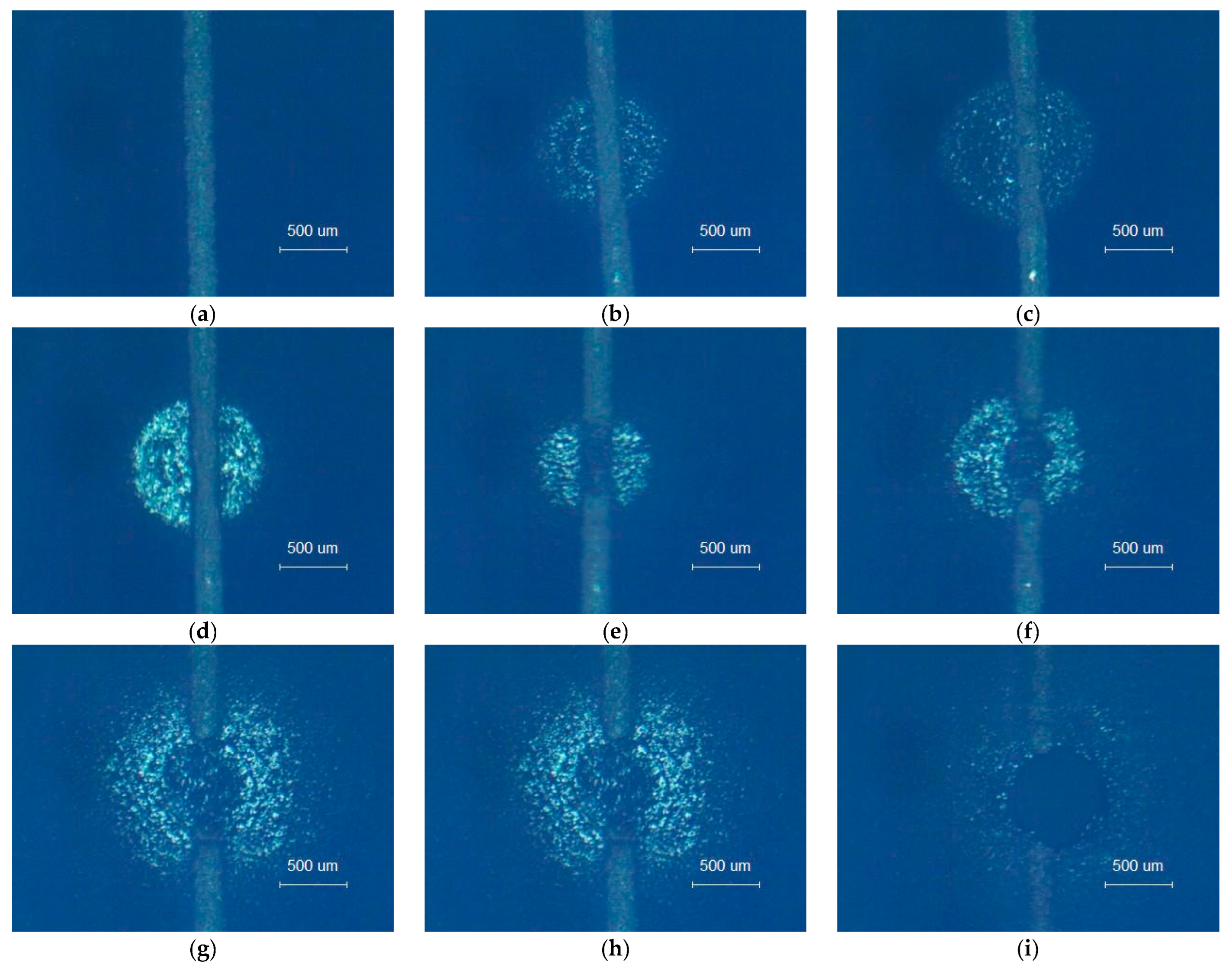
Figure 9 shows the surface morphology of the metal grid line electrode regions of the monocrystalline silicon cell after laser irradiation. In Figure 9b–d, it can be seen that the area of the heat-affected zone gradually increases as the laser fluence changes from 33.6 J/cm2 to 104.7 J/cm2. As shown in Figure 9e, when the laser fluence reaches 163.5 J/cm2, the metal grid line electrode begins to melt, with the area of the corresponding heat-affected zone decreasing. As the number of pulses increases, it can be observed that the metal grid line electrode has completely fractured and the area of the heat-affected zone increases rapidly again, as in Figure 9f–h. During this progress, the Pmax of the cell decreases significantly. This is due to the fracture of the grid line electrodes drastically reducing the absorption efficiency of the carriers inside the solar cells, resulting in more severe damage than in non-gridded areas. For multi-pulse irradiation, more and more heat will accumulate around the grid line electrodes, especially in a vacuum environment. The temperature of the material surface increases more rapidly, resulting in melting ablation craters, as shown in Figure 9i.
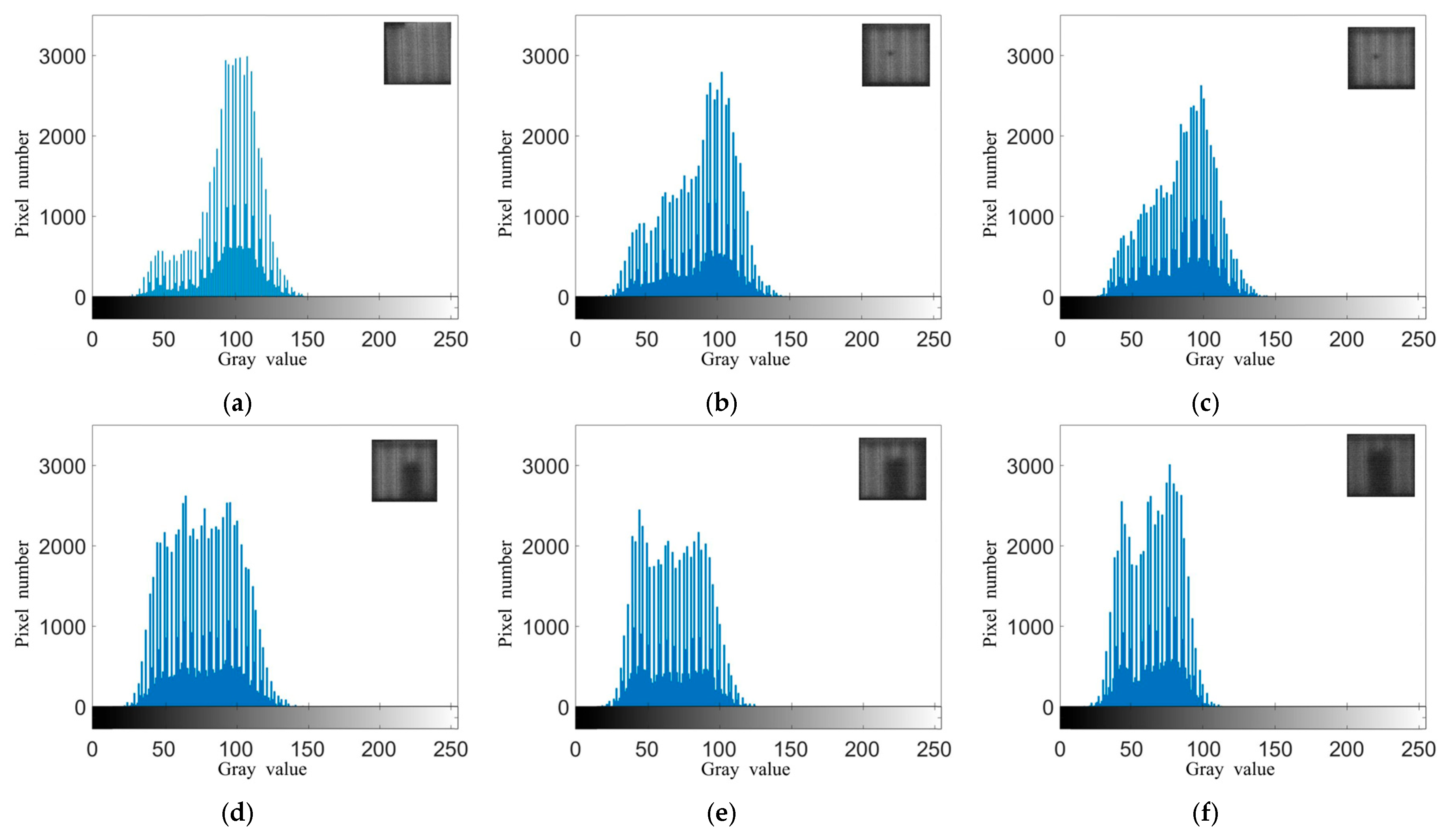
The EL images of the silicon cell after laser irradiation are shown in Figure 10. It can be seen that when the laser fluence is low, only a small area around the laser irradiation spot loses its luminescence ability. Once the grid line electrodes were damaged or even completely fractured, a large rectangular area between two neighboring grid line electrodes lost its luminescence ability. The gray histogram shifted significantly to the left after the fracture of the grid line electrode, which represented more severe damage to the cell. The decreasing trend of Pmax in Figure 11 aligns with the relative electroluminescence intensity, despite differences being present. Thus, the relative EL intensity of the monocrystalline silicon solar cells can reflect the variation of Pmax to some extent. Nevertheless, the difference between EL loss and power loss originates from EL’s exclusive sensitivity to bulk carrier recombination, whereas power loss integrates both the series resistance surge from grid fracture and the shunt resistance changes from lattice defects.

4. Discussion

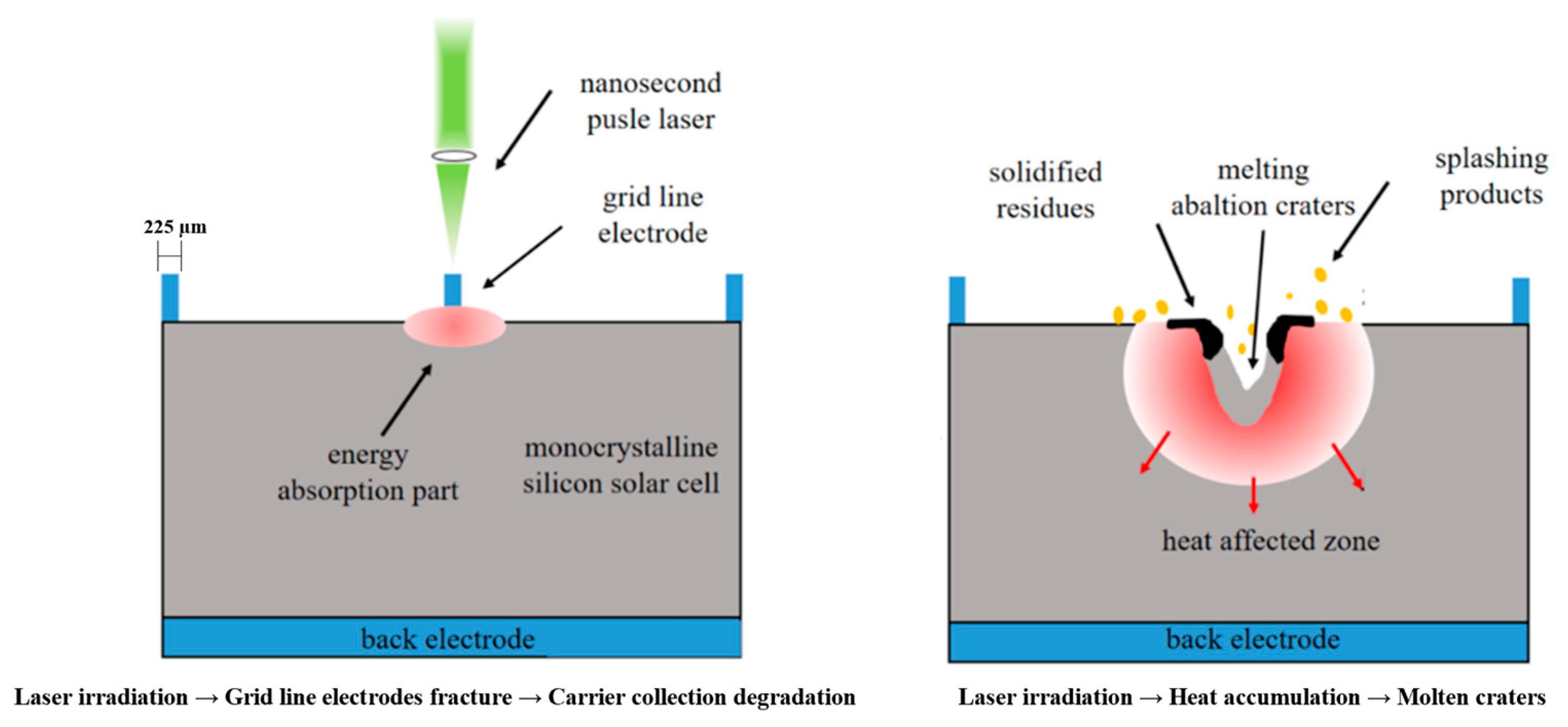
A schematic diagram of nanosecond laser damage to monocrystalline silicon cells is shown in Figure 12. The absorption mechanism of the monocrystalline silicon material for the laser is mainly the intrinsic absorption. During the electron transition from the valence band to the conduction band, electrons absorb energy from photons while transferring energy to the crystal lattices by emitting or absorbing phonons. Since the lattice energy relaxation time exceeds 10−12 s, the electrons fully transfer absorbed optical energy during 8 ns laser pulses. Consequently, thermal deformation first appears on cell surfaces, causing permanent performance degradation. With heat accumulation, surface melting occurs, accompanied by stress-induced cracks. Melting ablation craters and cracks disrupt the solar cell’s internal structure, creating failure zones.
It is worth noting that laser irradiation on metal grid line electrodes not only produces melting ablation craters and heat-affected zones but also fractures the grid line electrodes that are used for the carriers’ absorption. The variation in the Pmax of different laser irradiation positions is shown in Table 1. After sixteen pulses of each fluence at 165.3 J/cm2, the Pmax decreased by 42.6% for irradiation at the grid line electrodes, compared to 24.8% for irradiation at non-gridded line areas. The metal grid line electrodes fractured after four pulses of irradiation at 163.5 J/cm2, while the Pmax for non-gridded line areas only decreased by 15.8. Meanwhile, the electroluminescence images also showed that if the metal grid line electrode fractured, a large area around it would fail. Grid line fractures reduced the collection efficiency for carriers, which decreased the photovoltaic conversion capability of the solar cells, explaining the >20% higher Pmax degradation versus non-grid areas shown in Table 1. Therefore, it is essential to avoid laser irradiation at the metal grid line electrodes on the surface of the monocrystalline silicon cells, even if the laser influence is low.
The vacuum environment (10−3 Pa) also significantly changes heat dissipation dynamics and plasma behavior compared to atmospheric conditions. In ambient air, convective heat dissipation lowers surface temperatures and air breakdown plasma absorbs some of the incident laser energy [15]. This plasma quickly becomes superheated, creating shock waves and plasma sparks that cause mechanical damage and material ejection. Overall, the damage is due to thermal, shock, and mechanical factors for nanosecond and picosecond pulse width lasers. In the vacuum, the absence of plasma shielding and convective losses enabled near-total energy coupling to the silicon substrate, enabling non-gridline regions to withstand 163.5 J/cm2 (8 ns pulses) with only 24.8% Pmax degradation after 16 pulses. This direct comparison underscores the vacuum’s critical role in raising practical damage thresholds.

5. Conclusions

Laser irradiation position critically determines the damage severity in monocrystalline silicon solar cells under vacuum conditions. Avoiding laser exposure to gridline electrodes is essential, as the fracture of these structures disrupts carrier collection, causing significantly higher power degradation (>20%) compared to non-grid areas—even at identical fluences. Multi-pulse irradiation induces thermal accumulation, accelerating crater formation and stress cracking, while single pulses primarily cause surface oxidation. The strong correlation between the decline in electroluminescence intensity and Pmax loss confirms carrier recombination as the dominant failure mechanism. For space laser power systems, protecting gridlines through design or targeting strategies is a critical design consideration to maximize cell resilience.

Author Contributions

Conceptualization, H.C. and W.Z.; methodology, H.C.; validation, W.Z.; formal analysis, W.Z.; investigation, W.Z.; resources, H.C. and W.Z.; data curation, W.Z., Z.J., Y.M., X.Q. and C.X.; writing—original draft preparation, W.Z. and H.C.; writing—review and editing, H.C.; visualization, Z.J. and C.X.; funding acquisition, H.C. and W.Z. All authors have read and agreed to the published version of the manuscript.

Funding

This research was funded by the National Natural Science Foundation of China under Grant 11602304 and Grant 11502301.

Institutional Review Board Statement

Not applicable.

Informed Consent Statement

Not applicable.

Data Availability Statement

The data presented in this study are available on request from the corresponding author. Informed consent was obtained from all subjects involved in the study.

Acknowledgments

The authors would like to acknowledge Z.J. and C.X. for their assistance with the experiments.

Conflicts of Interest

The authors declare no conflicts of interest.

Abbreviations

The following abbreviations are used in this manuscript:
PVPhotovoltaic
ELElectroluminescence
VARVolt ampere relation

References

  1. Xiang, X.B.; Du, W.H.; Chang, X.L.; Yuan, H.R. The study on high efficient AlxGa1−xAs/GaAs solar cells. Sol. Energy Mater. Sol. Cells 2001, 68, 97–103. [Google Scholar] [CrossRef]
  2. Sharma, S.; Jain, K.K.; Sharma, A. Solar cells: In research and applications—A review. Mater. Sci. Appl. 2015, 6, 1145–1155. [Google Scholar] [CrossRef]
  3. Yamaguchi, M. High-efficiency GaAs-based solar cells. In Post-Transition Metals; IntechOpen: London, UK, 2020; pp. 107–128. [Google Scholar] [CrossRef]
  4. Battaglia, C.; Cuevas, A.; De Wolf, S. High-efficiency crystalline silicon solar cells: Status and perspectives. Energy Environ. Sci. 2016, 9, 1552–1576. [Google Scholar] [CrossRef]
  5. Jin, K.; Zhou, W. Wireless laser power transmission: A review of recent progress. IEEE Trans. Power Electron. 2018, 34, 3842–3859. [Google Scholar] [CrossRef]
  6. Dang, C.; Labie, R.; Tous, L.; Russell, R.; Recaman, M.; Deckers, J.; Uruena, A.; Duerinckx, F.; Poortmans, J. Investigation of laser ablation induced defects in crystalline silicon solar cells. Energy Procedia 2014, 55, 649–655. [Google Scholar] [CrossRef]
  7. Li, J.; Zhang, W.; Zhou, Y.; Zhang, X.; Jin, G. Experimental study of the damage morphology induced by the millisecond–nanosecond combined-pulse laser with different pulse delay on silicon. Optik 2021, 226, 165904. [Google Scholar] [CrossRef]
  8. Sun, Z.; Gupta, M.C. A study of laser-induced surface defects in silicon and impact on electrical properties. J. Appl. Phys. 2018, 124, 223103. [Google Scholar] [CrossRef]
  9. Li, S.; Huang, L.; Ye, J.; Hong, Y.; Wang, Y.; Gao, H.; Cui, Q. Study on Radiation Damage of Silicon Solar Cell Electrical Parameters by Nanosecond Pulse Laser. Electronics 2024, 13, 1795. [Google Scholar] [CrossRef]
  10. Qiu, D.; Jin, H.; Liu, S. Damage contrast of solar cells induced by short-pulse laser and CW Laser. Optoelectron. Technol. 2011, 31, 112–116. [Google Scholar] [CrossRef]
  11. Qiu, D.; Jin, H.; Sun, Y. Damage effects research of solar cells under the irradiation of 1064nm CW laser. Laser J. 2013, 34, 23–24. [Google Scholar] [CrossRef]
  12. Höhn, O.; Walker, A.W.; Bett, A.W.; Helmers, H. Optimal laser wavelength for efficient laser power converter operation over temperature. Appl. Phys. Lett. 2016, 108, 971–974. [Google Scholar] [CrossRef]
  13. Li, Y.; Zhang, J.; Dou, P.; Shi, Y.; Feng, G. Thermal damage mechanism of single junction GaAs solar cells irradiated by con-tinuous wave laser. Infrared Laser Eng. 2018, 47, 97–102. [Google Scholar] [CrossRef]
  14. Zhu, R.; Wang, R.; Cheng, X.; Xu, Z. Study of concentric iridescent ring around the laser-induced pits on the solar cell surface. Appl. Surf. Sci. 2015, 336, 375–379. [Google Scholar] [CrossRef]
  15. Wang, X.; Shen, Z.H.; Lu, J.; Ni, X.W. Laser-induced damage threshold of silicon in millisecond, nanosecond, and picosec-ond regimes. J. Appl. Phys. 2010, 108, 033103. [Google Scholar] [CrossRef]
  16. Yang, Y.; Lyu, T.; Zhang, R. Effect of repetition frequency laser on the response characteristics of silicon solar cell. Laser J. 2024, 1, 70–74. [Google Scholar] [CrossRef]
  17. Xue, Q.; Wu, W.; Ye, Y.; Liu, H.; Chen, R.; Hua, Y. Property degradation of GaAs/Ge solar cells after femtosecond laser irradiation. Laser Optoelectron. Prog 2015, 52, 122–128. [Google Scholar] [CrossRef]
  18. Guo, W.; Chang, H.; Yu, C.H.; Li, M.Y. Damage characteristics of continuous-wave laser ablation triple-junction solar cells. J. Laser Appl. 2022, 34, 042038. [Google Scholar] [CrossRef]
  19. Iwata, H.; Asakawa, K. Accumulative damage of GaAs and InP surfaces induced by Multiple-Laser-Pulse irradiation. Jpn. J. Appl. Phys. 2008, 47, 2161–2167. [Google Scholar] [CrossRef]
  20. Zhou, W.; Wen, M.; Chang, H.; Chen, Y.; Ji, G.; Ma, Y.; Jian, Z.; Liao, Y. Damage characteristics of solar cells irradiated by picosecond pulsed lasers. Infrared Laser Eng. 2023, 52, 20210870-1. [Google Scholar] [CrossRef]
  21. Matsuoka, Y.; Usami, A. Laser damage of silicon solar cells with different surface states. Opto-Electron. 1974, 6, 217–223. [Google Scholar] [CrossRef]
  22. Matsuoka, Y. Normal laser damage of silicon solar cells without phase change. Appl. Phys. Lett. 1974, 25, 574. [Google Scholar] [CrossRef]
  23. Matsuoka, Y.; Usami, A. Laser Damage of Silicon Solar Cells. J. Nucl. Sci. Technol. 1973, 10, 61–62. [Google Scholar] [CrossRef]
  24. Jia, Z.; Wang, W.; Li, X.; Hao, L. Millisecond laser-induced damage process of (001) silicon wafer. Opt. Eng. 2021, 60, 097101. [Google Scholar] [CrossRef]
  25. Schinke, C.; Christian Peest, P.; Schmidt, J.; Brendel, R.; Bothe, K.; Vogt, M.R.; Kröger, I.; Winter, S.; Schirmacher, A.; Lim, S.; et al. Uncertainty analysis for the coefficient of band-to-band absorption of crystalline silicon. AIP Adv. 2016, 5, 067168. [Google Scholar] [CrossRef]
  26. Fuyuki, T.; Kitiyanan, A. Photographic diagnosis of crystalline silicon solar cells utilizing electroluminescence. Appl. Phys. A 2009, 96, 189–196. [Google Scholar] [CrossRef]
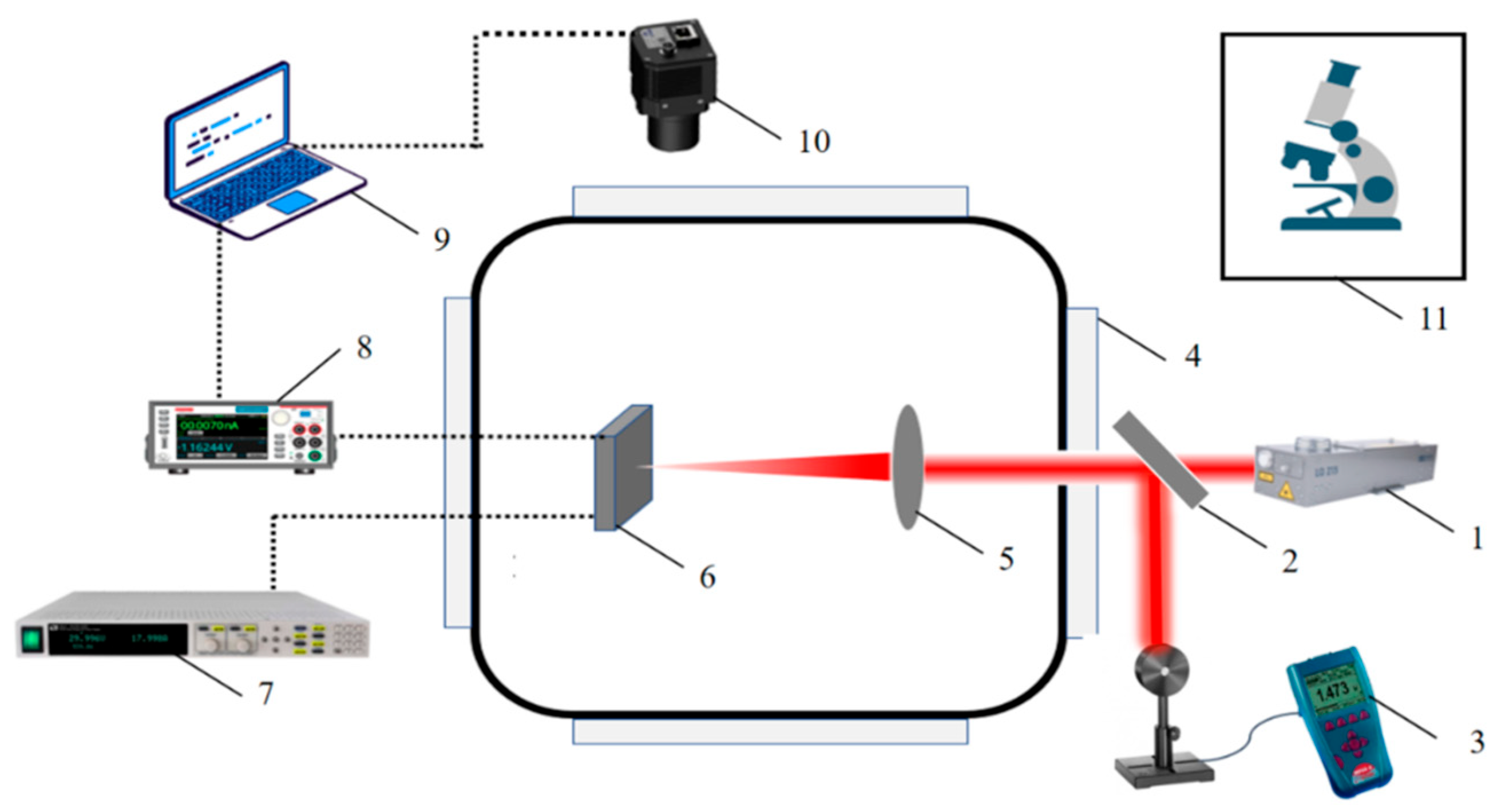
Figure 1. Schematic diagram of the experimental system of laser irradiation silicon solar cell: (1) Q-switched Nd: YAG laser; (2) beam splitter mirror; (3) laser energy meter; (4) vacuum chamber; (5) optical lens; (6) monocrystalline silicon solar cell; (7) DC power source; (8) digital source meter; (9) computer; (10) EL measurement camera; and (11) optical microscope.
Photonics 12 00804 g001
Figure 2. Schematic structure of monocrystalline silicon solar cell.
Photonics 12 00804 g002
Figure 3. Upper surface morphology of monocrystalline silicon cell sample.
Photonics 12 00804 g003
Figure 4. Changes in the electrical performance parameters of the silicon cell with nanosecond laser irradiated at non-gridded line areas: (a) volt–ampere relationship curves; and (b) power–voltage relationship curves.
Photonics 12 00804 g004
Figure 5. Surface morphology on non-gridded line areas of monocrystalline silicon cells irradiated by nanosecond laser. (a) Without laser irradiation; (b) Single pulse, with Laser fluence at 51.3 J/cm2; (c) Single pulse, with laser fluence at 104.7 J/cm2; (d) Single pulse, with laser fluence at 163.5 J/cm2; (e) Two pulses, each with a aser fluence at 163.5 J/cm2; (f) Four pulses, each with a laser fluence at 163.5 J/cm2; (g) Eight pulses, each with a laser fluence at 163.5 J/cm2; (h) Sixteen pulses, each with a laser fluence at 163.5 J/cm2.
Photonics 12 00804 g005
Figure 6. Pixel number distribution across gray values in the EL image after laser irradiation. (Inset: EL image of irradiated non-gridded line area). (a) Without laser irradiation; (b) Single pulse, with laser fluence at 51.3 J/cm2; (c) Single pulse, with laser fluence at 104.7 J/cm2; (d) Single pulse, with laser fluence at 163.5 J/cm2; (e) Four pulses, each with a laser fluence at 163.5 J/cm2; (f) Sixteen pulses, each with a laser fluence at 163.5 J/cm2.
Photonics 12 00804 g006
Figure 7. EL relative intensity and peak power of monocrystalline silicon cell after laser irradiation at non-gridded line areas: (a) different laser fluences; and (b) different pulse numbers with laser fluences at 163.5 J/cm2.
Photonics 12 00804 g007
Figure 8. Changes in electrical performance parameters of the silicon cell with nanosecond laser irradiated at metal grid line electrodes. (a) volt–ampere relationship curves. (b) power–voltage relationship curves.
Photonics 12 00804 g008
Figure 9. Surface morphology of the monocrystalline silicon cell after laser irradiation at metal grid line electrodes. (a) Without laser irradiation; (b) Single pulse, with laser fluence at 33.6 J/cm2; (c) Single pulse, with laser fluence at 51.3 J/cm2; (d) Single pulse, with laser fluence at 104.7 J/cm2; (e) Single pulse, with laser fluence at 163.5 J/cm2; (f) Two pulses, each with a laser fluence at 163.5 J/cm2; (g) Four pulses, each with a laser fluence at 163.5 J/cm2; (h) Eight pulses, each with a laser fluence at 163.5 J/cm2; (i) Sixteen pulses, each with a laser fluence at 163.5 J/cm2.
Photonics 12 00804 g009
Figure 10. Pixel number distribution across the gray value in the EL image after laser irradiation. (Inset: EL image of irradiated grid line area). (a) Without laser irradiation; (b) Single pulse, with laser fluence at 33.6 J/cm2; (c) Single pulse, with laser fluence at 104.7 J/cm2; (d) Single pulse, with laser fluence at 163.5 J/cm2; (e) Eight pulses, each with a laser fluence at 163.5 J/cm2; (f) Sixteen pules, each with a laser fluence at 163.5 J/cm2.
Photonics 12 00804 g010
Figure 11. EL relative intensity and peak power of monocrystalline silicon cell after laser irradiation at metal grid line electrodes: (a) different laser fluence; and (b) different pulse numbers with laser fluences at 163.5 J/cm2.
Photonics 12 00804 g011
Figure 12. Schematic diagram of nanosecond laser damage to monocrystalline silicon cells.
Photonics 12 00804 g012
Table 1. The decreasing rate of Pmax by nanosecond pulse laser irradiating at the grid line and in the non-gridded area, and their performance gaps.
Laser Fluence × Pulse NumberGrid Line ElectrodeNon-Gridded Line AreaPerformance Gap
5.8 J/cm2 × 11.0%0.0%1.0%
7.8 J/cm2 × 19.9%0.0%9.9%
33.6 J/cm2 × 110.9%0.0%10.9%
51.3 J/cm2 × 114.9%4.0%10.9%
104.7 J/cm2 × 121.8%6.9%14.9%
163.5 J/cm2 × 122.8%9.9%12.9%
163.5 J/cm2 × 226.7%11.9%14.8%
163.5 J/cm2 × 438.6%15.8%22.8%
163.5 J/cm2 × 843.6%19.8%23.8%
163.5 J/cm2 × 1642.6%24.8%17.8%
Disclaimer/Publisher’s Note: The statements, opinions and data contained in all publications are solely those of the individual author(s) and contributor(s) and not of MDPI and/or the editor(s). MDPI and/or the editor(s) disclaim responsibility for any injury to people or property resulting from any ideas, methods, instructions or products referred to in the content.