Abstract
Recently, diffractive optics systems have garnered increasing attention due to their myriad benefits in various applications, such as creating vortex beams, Bessel beams, or optical traps, while refractive optics systems still exhibit some disadvantages related to materials, substrates, and intensity shapes. The manufacturing of diffractive optical elements has become easier due to the development of lithography techniques such as direct laser writing, photo lithography, and electron beam lithography. In this paper, we improve the results from previous research and propose a new methodology to design and fabricate advanced binary diffractive optical elements that achieve a square focal spot independently, reducing reliance on additional components. By integrating a binary square zone plate with an axicon zone plate of the same scale, we employ machine learning for laser path optimization and direct laser lithography for manufacturing. This streamlined approach enhances simplicity, accuracy, efficiency, and cost effectiveness. Our upgraded binary diffractive optical elements are ready for real-world applications, marking a significant improvement in optical capabilities.
1. Introduction
Diffractive optical elements (DOEs) are designed to deflect light at specific angles and into certain orders. Additionally, DOEs have several advantages in creating unique focal points for various applications. For example, spiral DOEs can generate vortex beams [1,2], which are valuable in fields such as displacement measurement [3] and 3D magnetic imaging [4]. In addition, axicon DOEs [5,6] can be used to produce Bessel beams for applications such as those related to strong-field physics [7] and nanolithography [8]. DOEs can operate in non-light wavelengths, such as those associated with X-rays, [9,10] gamma rays [11], and ultraviolet light [12], where traditional lenses are challenging to manufacture due to material limitations. One intriguing application of DOEs relies on their capacity to create specialized focal shapes that traditional refractive optics struggle to produce. For example, DOEs can generate a circular focus via axicon zone plates (AZP) [5,6], vortex beams through spiral axicon zone plates [13], a cross-focus using square zone plates (SZPs) [14], and airy beams [15] as well. In prior research conducted by Sabatyan et al., a method for producing a square focus using a shifting-square zone plate (SSZP) was introduced [16]. The core concept of this study involved incorporating a shifting constant into the SZP to create a lateral phase shift, constrained along the horizontal and vertical axes according to a rectangular function. The research presented experimental results validating the proposed approach, which proved to be successful. However, the square focus generated in this study was notably large, with a focal length of 500 mm, which poses challenges for practical implementation in actual optical systems. Furthermore, the SSZP was fabricated using a printer, rendering it less suitable for professional optical applications. In our research, we aim to enhance this methodology by introducing new parameters that accommodate practical optical systems. Additionally, we present a novel technique for fabricating SSZPs that ensures their viability in real-world applications. To advance the generation of a square focus with a smaller beam size, we integrate the binary SZP with an AZP of the same scale, thereby broadening the potential applications of square beams and their future utility.
To design DOEs, various methods, such as computer-generated holography (CGH) [17,18] and/or the iterative Fourier transform algorithm (IFTA) [19,20], are used under help of programming languages such as MATLAB R2020b or Python. These designs often feature intricate shapes and detailed patterns at the micro- or nanoscale, which present considerable difficulties during their production. To maintain precision in the manufacturing stage, a technique that integrates Fourier optics, a machine-learning decision tree algorithm (MLDTA), and direct laser lithography (DLL) is employed to convert designs into real products. The effectiveness of DLL has been proven in numerous prior DOE manufacturing processes [21,22] and in various earlier studies [23,24]. MLDTA is widely recognized for its non-parametric supervised learning approach, which is adept at handling both classification and regression tasks [25,26]. In the manufacturing process, the MLDTA algorithm functions as a tool for generating laser paths for the DLL, utilizing the pixel matrix from the DOE. It effectively identifies which areas require laser processing and which ones should be skipped.
Initially, DOEs are developed using CGH or IFTA within the MATLAB R2020b environment. The resulting binary matrix is then transformed into laser path coordinates within the same platform, which enhances the accuracy of the MLDTA. In the subsequent step, these laser path coordinates are fed into the DLL system before the chemical etching process begins, leading to the creation of the final product. An optical verification system is established to assess the optical performance of the fabricated DOEs. This entire methodology is noted for its simplicity, dependability, and high precision when producing intricate DOE patterns. Additionally, it offers substantial benefits by minimizing labor and time demands while achieving very high fabrication success rates. Both the DLL system and the chemical etching solution are safe to handle, are cost-effective, and can be stored at room temperature without complications. Every aspect of the system can be adjusted using numerical methods, permitting customization to fulfill specific requirements. The entire design and laser path generation workflow is conducted within a single software platform, eliminating the need for external applications. Furthermore, this method allows for the creation of binary DOEs in various geometric shapes. The final products are compact, durable, and can be easily integrated into a range of optical systems without the need for supplementary optical components. This approach is particularly effective for generating binary DOEs and an assortment of patterns that are suitable for diverse applications such as beam shaping or laser heating manufacturing (laser plastic welding, glass frit sealing, laser bonding, or laser heaters).
2. Design Methodology
This section presents the creation of DOEs primarily based on CGH. The aim is to design and simulate the optical characteristics of these DOEs and to prepare the input matrix for further stages. In an earlier publication [27], Joseph W. Goodman provided an in-depth explanation of the physical process of holography, which involves two key phases: recording and reconstruction. The recording phase employs a standard technique known as interferometry. In this phase, a second wavefront coherent with the first and possessing a defined amplitude and phase is superimposed onto the unknown wavefront, as shown in Figure 1. The equation represents the object wave and represents the reference wave with which object wave interferes; then, the sum intensity of the interference is given by
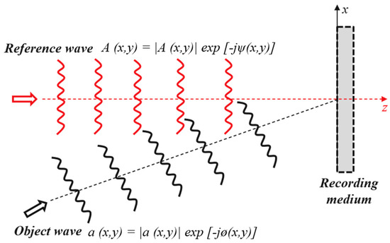
Figure 1.
Interferometric recording explanation.
The technique of recording the interference pattern produced by an object wave interacting with a reference wave can be seen as the creation of a hologram. This interference pattern is projected onto a photosensitive medium, and once developed, the resulting amplitude transmittance of the hologram corresponds to the intensity distribution of the interference pattern. When the hologram is illuminated by the reference wave, it generates the object wave, and the same principle applies in reverse.
For CGH, the interference pattern produced by the computer programming language is transformed into a corresponding phase profile, which can then be represented in binary, multilevel, or grayscale formats. In previous research conducted by S. Bhattacharya and A. Vijayakumar, insights were shared regarding the creation of DOEs using CGH [28]. Conceptually, CGH is an interferogram formed by the overlapping of two waves. For example, when a plane wave A (as described in Equation (2)) interferes with a conical wave B (as presented in Equation (3)), which travels at an angle “θ” along the z-axis, the result is an AZP pattern (Figure 2), which will appear later in this section, assuming both waves share the same constant amplitude profile.
where is the tilt angle of the wave, x and y are the coordinates, and is the wavelength. When a plane wave strikes a refractive axicon at a right angle, it produces a conical wave. This conical wavefront shows a gradual change in phase along the radial direction, resulting in a fringe pattern that is evenly spaced in that same direction.
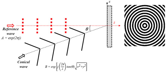
Figure 2.
AZP formation by a conical wave and a reference wave.
Similarly, the proposal to establish an SSZP put forth by Sabatyan et al. [16] introduces the incorporation of a shifting constant (which affects the shifting on the focused intensity) and the side length into the existing SZP equation. As a result, the modified equation takes the following form:
where is the wavelength, is the focal length, L is the dimension of the SSZP, and x and y are the coordinates. The binary classification and rectangle function are described below:
In their study, Sabatyan et al. [16] set L to 12 mm and f to 500 mm, which may be quite large for an optical system. Therefore, it is better to scale down the parameters to achieve a shorter focal length for good agreement with actual optical systems. The simulation results (with the same wavelength of 632.8 nm) and an example of new parameters are displayed in Figure 3. In order to evaluate the optical performance of the SSZP or any DOE, we utilize the “Fresnel impulse response propagator” approach (the choice of propagation methods may vary based on the dimensions and propagation distance utilized in the experimental section that follows; different approaches may be considered if the conditions require it). This method allows us to model the optical characteristics of every DOE by employing the theoretical framework provided by Rayleigh–Sommerfeld diffraction solution I [29]:
whilst the general form of the Rayleigh–Sommerfield impulse response is as follows:
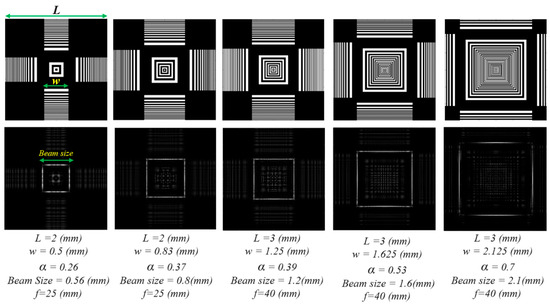
Figure 3.
SSZP patterns (above line) and their intensity simulation result (below line).
Here, the values of represent the complex field amplitude in the source (source plane), those of (the result of the propagation process) signify the field retrieved after propagating the source plane over a distance of z (mm), and
As a result, the SSZP is now optimized for practical applications in real-world systems. In the subsequent section, we present an innovative fabrication method for the SSZP that does not rely on conventional printer imaging techniques, as referenced in earlier work [16]. However, it is important to note that generating smaller square focal points poses significant challenges due to the limitations imposed by the shifting constant. Specifically, as the parameter is decreased, the fidelity of the square shape diminishes, resulting in a configuration that resembles a cross rather than a true square, as discussed in the aforementioned study [16]. To address this limitation, we propose a novel approach that combines the capabilities of the AZP and the SZP and then applies the binary classification in Equation (5). The resulting fused DOE enables the creation of smaller square beams across a range of focal lengths. The mathematical formulations required to derive the AZP is described in Equation (3) and SZP are detailed below.
In addition, another effect in Equation (3) is determining the number of circles in an AZP. The results are displayed in Figure 4, while the design parameters are shown in Table 1. By increasing or decreasing the L and changing θ, it may lead to an increase or decrease in the beam size and focal length, respectively. It should be noted that the matrix dimension refers to the number of rows and columns in the DOE matrix. The pixel pitch, which represents the resolution, is equal to L divided by the matrix dimensions. These parameters significantly impact the fabrication process, as discussed later.
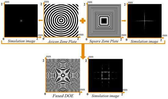
Figure 4.
Square-focus formation by fusing AZP and SZP.

Table 1.
Fused DOE parameters.
The design of new DOE or other variants can be meticulously crafted by calibrating the parameters based on empirical knowledge and experimentation. However, the process of achieving an optimal balance among these input parameters can often be time-consuming and labor-intensive. For instance, in the context of this research, when certain conditions such as the wavelength, pixel pitch, and matrix dimensions are held constant (due to the equipment), the parameters L, , and f play a significant role in influencing the design. The challenges associated with balancing and predicting these parameters to align with the design specifications can be formidable. Therefore, we propose a methodology aimed at streamlining this process, thereby reducing both the time and effort required to achieve optimal design outcomes.
The foundation of this method is based on forecasting parameters using a machine learning regression algorithm. Depending on the trends identified in the training data, various regression methods can be applied, with Linear Regression [30] being the simplest option. For instance, in this research, we utilized Multivariate Polynomial Regression (MPR) [31] to address the problem due to the trend in training data. MPR expands upon Linear Regression by accommodating multiple input variables and allowing for non-linear interactions between those variables and the outcome variable (Figure 5). In this model, the input variables are taken to various powers, resulting in a polynomial equation. The coefficients in this polynomial equation are estimated through a least-squares optimization method, similar to the approach used in Linear Regression.
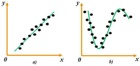
Figure 5.
(a) Linear Regression. (b) Polynomial Regression. The black dots represent the data while the green line is the regression line.
The mathematical expression for MPR [31] is described below.
Here, y is the dependent variable, and x is the independent variable. , , … are the coefficients of the polynomial terms, k is the degree of the polynomial, and represents the error term. In addition, the model can be shown as a system of linear equations, as follows:
The estimated Polynomial Regression coefficients vector is calculated using the equation below.
In the design of fused DOEs, several critical parameters, specifically f, L, and the , influence the design process profoundly. A comprehensive dataset comprising the specifications of 30 distinct DOEs, each characterized by varying the values of f, L, and , has been developed. This dataset facilitates the generation of square focal spots at various distances and beam sizes, as detailed in Table 2. The dataset can be employed to predict one parameter based on two given parameters. For instance, during the design of fused DOEs, it is common practice to specify f and L, thereby allowing for the estimation of using the dataset in conjunction with MPR. This approach significantly minimizes the computational time. It is important to note that the accuracy of the dataset directly impacts the quality of the predictions. Additionally, the selected parameters must remain within reasonable bounds to uphold the correlative relationship between the dimensions of the DOE and its focal length. For example, maintaining a long focal length with a small DOE presents significant challenges. Moreover, this predictive methodology can be generalized to various designs of DOEs, provided that the dataset is precise and the given parameters are both qualitatively and quantitatively suitable. Although Linear Regression could also be applied to this dataset, preliminary assessments indicate that its predictive performance is inferior to that of MPR, as the interactions between the parameters in the context of fused DOEs exhibit non-linear characteristics.
Table 2.
Training dataset.
Figure 6 presents the simulation results for five fused DOEs with randomly assigned values for f and L, along with the predicted generated by the MPR algorithm. It is evident that the algorithm performs well with this dataset, as the square beam produced is significantly smaller compared to the design method developed by Sabatyan et al. The SSZP and fused DOE fabrication process is discussed in the next section. In addition, using L values of 2 or 3 mm, the previous method creates a DOE that generates beams ranging from 0.56 mm to 2.1 mm. In our design, with L values of 2.52 mm, 4.3 mm, and even 5.2 mm, we generate beams with sizes of 0.38 mm, 0.6 mm, and 0.7 mm, respectively.
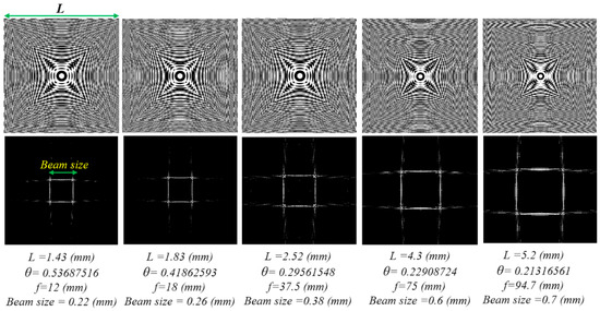
Figure 6.
Fused DOE simulation results and corresponding design parameters.
3. Fabrication Process
In the previous section, a binary matrix was obtained, which enables the direct generation of laser paths in MATLAB R202b without the need for additional software. This approach offers precise control over all parameters, ensuring the efficiency of the system. The explanation of this method is introduced in Figure 7a.
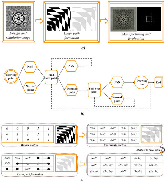
Figure 7.
(a) The overall process from design, fabrication, and evaluation. (b) Laser path generating algorithm explanation. (c) Laser path construction.
The algorithm for generating laser paths utilizes the MLDTA approach, where decisions are made based on a classification method. In MATLAB, DOEs are represented as a matrix, with each pixel corresponding to a specific value. For binary DOEs, pixel values can only be 0 or 1. Leveraging this framework, we can design an algorithm that populates all pixels with a value of 1 while ignoring those that are 0 (Figure 7b). This algorithm is capable of scaling the design to actual dimensions. Such a straightforward yet effective method for fabricating DOEs is particularly advantageous for applications involving laser lithography or laser writing. It proves especially useful for custom systems, as it helps minimize costs and removes the necessity of acquiring costly commercial machinery.
To start, the pixel positions from the binary matrix are converted into the coordinates for the DOE pattern. Pixels with a value of 0 are designated as NaN (Not a Number), while the positions of pixels with a value of 1 are used to construct the coordinate matrix. This matrix is then scaled according to the pixel pitch specified for each DOE, translating the coordinates into “real-life” dimensions suitable for the DLL machine. MLDTA is then employed to scan each row (or column), linking all points while skipping NaN points to streamline the calculation and minimize manufacturing time. The coordinates that correspond to the laser paths are subsequently sent to the DLL system for the production of the DOE patterns, as depicted in Figure 7c. The entire computational process, from Section 2 to the generation of all laser path coordinates in Section 3, was efficiently completed using MATLAB on a laptop in just a few seconds (Dell Technologies, Round Rock, TX, USA—Dell Latitude 7390 2018-United States Intel Core i7-8650U CPU @ 1.90 GHz 2.11 GHz, 16 GB of RAM).
In the diagram depicted in Figure 8a, the operation of the DLL system is illustrated. Initially, a laser source (1) is employed to generate the laser beam. Subsequently, an acousto-optic modulator (2) regulates the intensity of the beam prior to its passage through the shutter (3). The shutter is capable of obstructing the beam path as necessary, after which three mirrors (4, 5, 6) redirect the laser beam toward the writing head (7). The specimen (8) is securely positioned on linear stages X and Y (9, 10). The entirety of the system is integrated with the control system (11).
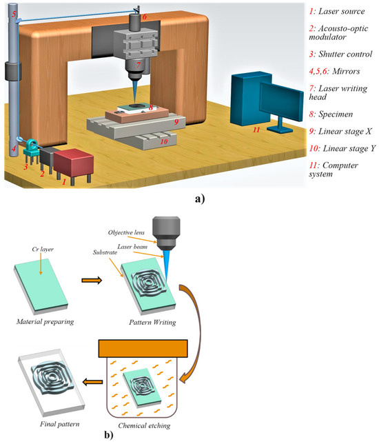
Figure 8.
(a) DLL system, (b) chemical etching process.
The process of fabricating DOEs by the DLL system is illustrated in Figure 8b. Initially, a glass substrate with a refractive index of approximately 1.5 and a Chromium (Cr) layer on its surface is prepared. Subsequently, laser paths from the previous section are imported into the DLL system to inscribe the desired pattern on the surface. The laser beam (514.5 nm) induces the conversion of Cr into Chromium (III) Oxide (Cr2O3). The substrate material is selected for its durability, affordability, and ease to etch, while the wavelength is chosen to optimize the substrate’s performance. Other wavelengths, such as 400, 800, and 1030 nm, as well as substrates like polymer and silicone, can be utilized in a custom direct laser lithography machine. In addition, modern techniques can be used for custom direct laser lithography writing in DOE fabrication, such as multiphoton lithography [32] or metasurfaces [33]. Following this, the specimen undergoes a five-minute etching process in a chemical solution (formed by mixing one solution containing 37.5 g K3Fe(CN)6 with 100 mL pure water and the other containing 6.25 g NaOH with a 25 mL pure water solution) to remove the Cr layer while preserving the Cr2O3. This completes the fabrication of the DOEs.
The outcomes of the fabrication process, as detailed in Section 1, are depicted in Figure 9. We choose an SSZP with L = 2 mm, w = 0.83 mm, = 0.37, and f = 25 mm, along with the fused DOE, as described in Table 1. Upon an initial examination, both the SSZP and fused DOE surfaces appear smooth and clean, with their geometries perfectly matching the simulations. The subsequent section will delve into an evaluation process aimed at assessing the surface quality and optical performance of each DOE.
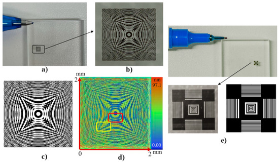
Figure 9.
Fabrication results: (a) fused DOE specimens, (b) zoomed-in view, (c) simulation image, (d) surface quality, and (e) SSZP specimen (left) and corresponding simulation image (right).
4. Experimental Results and Optical Evaluation
In this section, we present a comprehensive analysis of the surface measurement results and optical performance of each DOE. The surface measuremenst was conducted using a commercial white-light scan uncontacted interferometer, Nano System NV-2400 (Nano System Company, Daejeon, Republic of Korea). Figure 10 and Figure 11 present the detailed surface quality measurement of the fused DOE in Figure 9d. The results from the manufacturing process demonstrate exceptional surface quality levels, with the geometrical configurations of the fused DOE aligning precisely with the design specifications outlined in the preceding section.
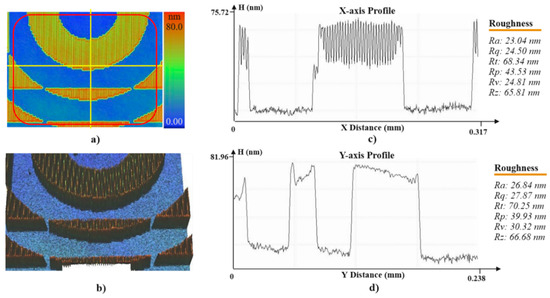
Figure 10.
(a) Local view (red) of Figure 9d, (b) 3D view, and (c,d) surface profile on the X and Y axes in (a).
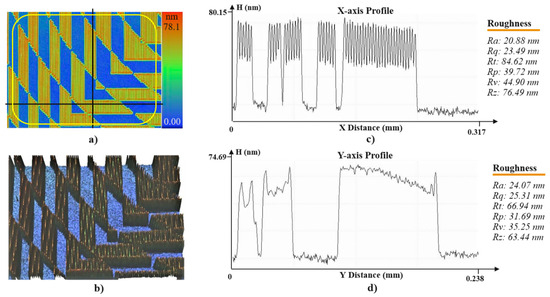
Figure 11.
(a) Local view (yellow) of Figure 9d, (b) 3D view, and (c,d) surface profile on X and Y axes in (a).
To verify the optical performance of the DOEs, an optical system was meticulously assembled (Figure 12a). This system utilized a He-Ne laser (1) as a beam source with a precise wavelength of 632.8 nm. To adapt the intensity for the CMOS camera, a meticulous approach was employed, involving the use of two lenses (2, 3) to expand the laser beam and a filter (4). Specifically, the experiment utilized a Thorlabs AC254-030-A-ML lens (with a focal length of 30 mm and a diameter of 25.4 mm, BBARR COATING 400–700 nm, N-BAF10/N-SF6HT, Thorlabs Inc., Newton, NJ, USA) and a Thorlabs AC254-300-A-ML lens (with a focal length of 300 mm and a diameter of 25.4 mm, BBARR COATING 400–700 nm, N-BK7/SF2. Thorlabs Inc, Newton, NJ, USA). The specimen (5) was positioned precisely in front of the CMOS camera (6) on a movable stage. Notably, it is imperative to highlight that no additional equipment was employed to enhance the performance of the DOEs, thus ensuring that the experimental results are a true representation of the DOEs’ performance capabilities.
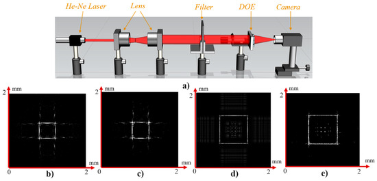
Figure 12.
(a) Optical verification setup, (b) fused DOE simulation image, (c) fused DOE experiment image, (d) SSZP simulation image, and (e) SSZP experiment image.
The experimental images demonstrate a strong correlation with the simulation results, thereby validating the accuracy of the design, simulation, and fabrication processes (Figure 12b–e). These findings substantiate the precision of these methodologies, highlighting their relevance and applicability across a variety of contexts in both research and industrial settings, particularly for the development and evaluation of DOEs. This thorough assessment underscores the potential to advance methodologies within the fields of optical engineering and manufacturing, paving the way for enhanced innovation and efficiency.
5. Conclusions
In this manuscript, we present methods for generating square-focus configurations using DOEs. These DOEs can create square-focus configurations in various dimensions and focal lengths, making them suitable for real-life applications. In addition, the design and fabrication process overcome the drawbacks of previous methods and improve square-focus generating by DOEs.
The design and optical performance of the DOEs are simulated using advanced methods, in this case CGH, IFTA, or other Fourier optics techniques. Subsequently, laser path coordinates are derived from the simulated binary matrix result by MLDTA. In the subsequent stage, a DLL system is employed to fabricate the DOEs before etching using a chemical solution. Finally, the surface of the DOEs is characterized and the optical performance is verified to ensure the precision of the design and fabrication processes.
The resulting DOEs exhibit small, compact, and durable characteristics, with shapes and optical performance congruent with the design and simulation process. Furthermore, the DOEs are ready for integration into any optical system without the need for additional optical equipment. The design process is characterized by simplicity, efficiency, and self-containment within one software package, ensuring accuracy when transferring from simulation results to laser path coordinates without the requirement of expensive equipment or external software. The DLL system does not require a mask or a cleanroom, making it cost effective for manufacturing and maintenance. Additionally, the etching chemical solution is non-toxic, cost-efficient, readily available, and stable for long-term storage under standard room conditions. The DOEs feature the ability to manipulate the intensity independently without the need for additional equipment. Their compact, durable, and cost-effective design enhances their applicability in real-world optical systems. Furthermore, this methodology simplifies the production of high-resolution binary DOEs with intricate patterns and superior optical characteristics.
Author Contributions
Conceptualization, H.T.D.T., Y.-S.G. and H.-G.R.; Methodology, Y.-S.G. and H.-G.R.; Software, H.T.D.T.; Validation, Y.-S.G. and H.-G.R.; Formal analysis, H.T.D.T.; Investigation, H.T.D.T. and H.-G.R.; Resources, H.-G.R.; Data curation, H.T.D.T.; Writing—original draft, H.T.D.T.; Writing—review & editing, Y.-S.G. and H.-G.R.; Visualization, H.T.D.T.; Supervision, Y.-S.G. and H.-G.R.; Project administration, H.-G.R.; Funding acquisition, H.-G.R. All authors have read and agreed to the published version of the manuscript.
Funding
This work was supported in part by the Technology Innovation Program (grant no. RS-2023-00237714, Development of Dynamic Metrology Tool for CMP Process Stabilization) funded by the Ministry of Trade, Industry & Energy (MOTIE, Korea) (NTIS no. 1415187786) and in part by the Technology Innovation Program (grant no. 20020311, Optical Technology for the Automatic Analysis of EUV Mask) funded by the Ministry of Trade, Industry & Energy (MOTIE, Republic of Korea).
Data Availability Statement
Data will be made available on request.
Conflicts of Interest
The authors declare no conflict of interest.
References
- Jiménez, N.; García, V.R.; Raffi, L.M.G.; Camarena, F.; Staliunas, K. Sharp acoustic vortex focusing by Fresnel-spiral zone plates. Appl. Phys. Lett. 2018, 112, 204101. [Google Scholar] [CrossRef]
- Zhang, L.; Zhang, H.; Huang, H.; Wang, J.; Zhou, H.; Yu, T. Generation of ultra-intense vortex laser from a binary phase square spiral zone plate. Opt. Express 2024, 32, 5161–5173. [Google Scholar] [CrossRef]
- Gao, H.; Hu, X.; Yang, Z.; Liu, Z. Application of vortex beam interference in displacement measurement. In Proceedings of the Fourteenth International Conference on Information Optics and Photonics (CIOP 2023), Xi’an, China, 24 November 2023; Proceedings SPIE: Bellingham, WA, USA, 2023; Volume 12935. [Google Scholar] [CrossRef]
- Barrows, F.; Petford-Long, A.K.; Phatak, C. 3D magnetic imaging using electron vortex beam microscopy. Commun. Phys. 2022, 5, 324. [Google Scholar] [CrossRef]
- Khonina, S.N.; Kazanskiy, N.L.; Khorin, P.A.; Butt, M.A. Modern Types of Axicons: New Functions and Applications. Sensors 2021, 21, 6690. [Google Scholar] [CrossRef]
- Vijayakumar, A.; Bhattacharya, S. Phase-shifted Fresnel axicon. Opt. Lett. 2012, 37, 1980–1982. [Google Scholar] [CrossRef] [PubMed]
- Summers, A.M.; Yu, X.; Wang, X.; Raoul, M.; Nelson, J.; Todd, D.; Zigo, S.; Lei, S.; Trallero-Herrero, C.A. Spatial characterization of Bessel-like beams for strong-field physics. Opt. Express 2017, 25, 1646–1655. [Google Scholar] [CrossRef] [PubMed]
- Fan, D.; Wang, L.; Ekinci, Y. Nanolithography using Bessel Beams of Extreme Ultraviolet Wavelength. Sci. Rep. 2016, 6, 31301. [Google Scholar] [CrossRef]
- Chang, C.; Sakdinawat, A. Ultra-high aspect ratio high-resolution nanofabrication for hard X-ray diffractive optics. Nat. Commun. 2014, 5, 4243. [Google Scholar] [CrossRef]
- Marchesini, S.; Sakdinawat, A. Shaping coherent x-rays with binary optics. Opt. Express 2019, 27, 907–917. [Google Scholar] [CrossRef]
- Skinner, G.K. Design and imaging performance of achromatic diffractive—refractive x-ray and gamma-ray Fresnel lenses. Appl. Opt. 2004, 43, 4845–4853. [Google Scholar] [CrossRef] [PubMed]
- Feng, S.; Wang, Z.; Cheng, X.; Dun, X. Design of diffractive optical element for ultra-thin deep ultraviolet imaging system. In Proceedings of the International Conference on Optoelectronic and Microelectronic Technology and Application, Nanjing, China, 20–22 October 2020; SPIE: Bellingham, WA, USA, 2020; Volume 11617, pp. 560–567. [Google Scholar] [CrossRef]
- Nalimov, A.; Stafeev, S.; Kotlyar, V.; Kozlova, E. Optical Sensor Methodology for Measuring Shift, Thickness, Refractive Index and Tilt Angle of Thin Films. Photonics 2023, 10, 690. [Google Scholar] [CrossRef]
- Alda, J.; Rico-García, J.M.; Salgado-Remacha, F.J.; Sanchez-Brea, L.M. Diffractive performance of square Fresnel zone plates. Opt. Commun. 2009, 282, 3402–3407. [Google Scholar] [CrossRef][Green Version]
- Trung, H.T.D.; Ghim, Y.S.; Rhee, H.G. Design and Fabrication of Micro-binary Diffractive Optical Elements to Generate Airy Beams Using a Versatile Direct Laser Lithography Machine. Curr. Opt. Photon. 2025, 9, 130–140. [Google Scholar] [CrossRef]
- Sabatyan, A.; Taheri Balanoji, S.M. Square-shaped beam generated by phase shifted bounded square zone plate. Opt. Quantum Electron. 2017, 49, 325. [Google Scholar] [CrossRef]
- Cederquist, J.N.; Fienup, J.R. Analytic design of optimum holographic optical elements. J. Opt. Soc. Am. A 1987, 4, 699–705. [Google Scholar] [CrossRef]
- Feldman, M.R.; Guest, C.C. Computer generated holographic optical elements for optical interconnection of very large scale integrated circuits. Appl. Opt. 1987, 26, 4377–4384. [Google Scholar] [CrossRef] [PubMed]
- Wyrowski, F.; Bryngdahl, O. Iterative Fourier-transform algorithm applied to computer holography. J. Opt. Soc. Am. A 1988, 5, 1058–1065. [Google Scholar] [CrossRef]
- Hasegawa, S.; Nozaki, K.; Tanabe, A.; Hashimoto, N.; Hayasaki, Y. Holographic femtosecond laser processing using 6.3 kHz pulse-to-pulse spatial light modulation with binary phase masks. Opt. Laser Technol. 2024, 176, 111014. [Google Scholar] [CrossRef]
- Trung, H.T.D.; Nguyen, H.L.V.; Munnibee, A.; Kim, Y.-J.; Ghim, Y.-S.; Rhee, H.G. Design and fabrication of a Fresnel zone plate with an enhanced depth of focus. Appl. Opt. 2024, 63, 6384–6392. [Google Scholar] [CrossRef]
- Anh, N.N.H.; Rhee, H.; Ghim, Y.S. Novel fabrication and designs for hybrid optical elements with wider angle field of view by using integrated direct laser lithographic system. Opt. Lasers Eng. 2023, 170, 107774. [Google Scholar] [CrossRef]
- Song, Y.; Xu, J.; Liu, Z.; Zhang, A.; Yu, J.; Qi, J.; Chen, W.; Cheng, Y. Fabrication of high-aspect-ratio fused silica microstructures with large depths using Bessel-beam femtosecond laser-assisted etching. Opt. Laser Technol. 2024, 170, 110305. [Google Scholar] [CrossRef]
- Yang, Y.; Li, S.; Xu, H.; Xu, Y.; Chen, Y. Fabrication of flexible microheater with tunable heating capabilities by direct laser writing and selective electrodeposition. J. Manuf. Process. 2022, 74, 88–99. [Google Scholar] [CrossRef]
- Rahman, M.; Kamal, N.; Abdullah, N.F. EDT-STACK: A stacking ensemble-based decision trees algorithm for tire tread depth condition classification. Results Eng. 2024, 22, 102218. [Google Scholar] [CrossRef]
- Alrbai, M.; Al-Dahidi, S.; Alahmer, H.; Al-Ghussain, L.; Hayajneh, H.; Shboul, B.; Abusorra, M.; Alahmer, A. Utilizing waste heat in wastewater treatment plants for water desalination: Modeling and Multi-Objective optimization of a Multi-Effect desalination system using Decision Tree Regression and Pelican optimization algorithm. Therm. Sci. Eng. Prog. 2024, 54, 102784. [Google Scholar] [CrossRef]
- Goodman, J.W. Introduction to Fourier Optics, 2nd ed.; McGraw-Hill Companies Inc.: New York, NY, USA, 1996. [Google Scholar]
- Vijayakumar, A.; Bhattacharya, S. Design and Fabrication of Diffractive Optical Elements with MATLAB; SPIE: Bellingham, WA, USA, 2017; ISBN 9781510607064. [Google Scholar] [CrossRef]
- Voelz, D.G. Computational Fourier Optics: A MATLAB Tutorial 2011; SPIE Press: Bellingham, WA, USA, 2011; pp. 52+64–66. ISBN 9780819482044. [Google Scholar]
- Hope, T.M. Linear regression. Machine Learning: Methods and Applications to Brain Disorders; Academic Press: Cambridge, MA, USA, 2019; pp. 67–81. [Google Scholar] [CrossRef]
- Priyanka, S. Multivariate Polynomial Regression in Data Mining: Methodology, Problems and Solutions. Int. J. Sci. Eng. Res. 2013, 4, 962–965. [Google Scholar]
- Zuev, D.M.; Nguyen, A.K.; Putlyaev, V.I.; Narayan, R.J. 3D printing and bioprinting using multiphoton lithography. Bioprinting 2020, 20, e00090. [Google Scholar] [CrossRef]
- Bochek, D.V.; Samusev, K.B.; Yavsin, D.A.; Zhukov, M.V.; Limonov, M.F.; Rybin, M.V.; Shishkin, I.I.; Sinelnik, A.D. Fabrication of Ge2Sb2Te5 metasurfaces by direct laser writing technique. Opt. Laser Technol. 2021, 141, 107124. [Google Scholar] [CrossRef]
Disclaimer/Publisher’s Note: The statements, opinions and data contained in all publications are solely those of the individual author(s) and contributor(s) and not of MDPI and/or the editor(s). MDPI and/or the editor(s) disclaim responsibility for any injury to people or property resulting from any ideas, methods, instructions or products referred to in the content. |
© 2025 by the authors. Licensee MDPI, Basel, Switzerland. This article is an open access article distributed under the terms and conditions of the Creative Commons Attribution (CC BY) license (https://creativecommons.org/licenses/by/4.0/).