Abstract
Experimental and simulation analysis was conducted on the effects of 532 nm nanosecond laser-induced thermal damage on the front-side illuminated CMOS detector. The study examined CMOS detector output images at different stages of damage, including point damage, line damage, and complete failure, and correlated these with microscopic structural changes observed through optical and scanning electron microscopy. A finite element model was used to study the thermal–mechanical coupling effect during laser irradiation. The results indicated that at a laser energy density of 78.9 mJ/cm2, localized melting occurs within photosensitive units in the epitaxial layer, manifesting as an irreversible white bright spot appearing in the detector output image (point damage). When the energy density is further increased to 241.9 mJ/cm2, metal routings across multiple pixel units melt, resulting in horizontal and vertical black lines in the output image (line damage). Upon reaching 2005.4 mJ/cm2, the entire sensor area failed to output any valid image due to thermal stress-induced delamination of the silicon dioxide insulation layer, with cracks propagating to the metal routing and epitaxial layers, ultimately causing structural deformation and device failure (complete failure).
1. Introduction
The Complementary Metal-Oxide-Semiconductor (CMOS) is a solid-state imaging device that converts optical signals into electrical signals through a photodiode array [1]. Compared to Charge Coupled Devices (CCDs), CMOS devices reduce system complexity and power consumption while offering high quantum efficiency, wide dynamic response, and superior anti-crosstalk performance [2]. These advantages have led to CMOS devices gradually replacing CCDs in applications such as intelligent surveillance [3], space remote sensing [4], and automotive applications [5]. However, the multilayer structure of CMOS devices, composed of metal and silicon materials, is susceptible to damage from high-intensity laser irradiation. This can cause signal distortion, structural damage, and interlayer delamination [6]. Research on the mechanisms of laser-induced damage in CMOS devices is essential for designing robust imaging systems and developing laser protection strategies for photodetectors.
Researchers have conducted experimental studies to investigate the impact of different laser parameters on the damage characteristics of the detector. Wang et al. compared continuous-wave (CW) lasers with single-pulse nanosecond lasers and found that pulsed lasers had a significantly lower energy density threshold for CMOS damage [7]. Schwarz et al. used the 1-on-1 test method to measure damage thresholds of picosecond and nanosecond pulsed lasers on CMOS cameras, with picosecond lasers showing a lower damage threshold [8,9]. Westgate et al. demonstrated that back-side illuminated (BSI) CMOS requires two orders of magnitude higher laser energy density for complete damage than front-side illuminated (FSI) CMOS, due to its circuitry placement beneath the photosensitive layer [10]. Cao et al. demonstrated that combined nanosecond/picosecond laser irradiation induced damage to CCD detectors, achieving a complete damage threshold of 103 mJ/cm2—significantly lower than thresholds observed under single nanosecond or picosecond laser pulses [11]. Yoon et al. found that CMOS damage from CW near-infrared laser irradiation had reversible interference at low energy densities and irreversible damage at higher energy densities [12]. Théberge et al. used different CW lasers to damage silicon-based cameras, categorizing damage into three stages based on pixel response degradation, circuit layer melting, and sensor failure [13]. Wang et al. studied CMOS devices with mid-infrared lasers, observing saturation, black screen, and other damage phenomena [14]. Xu et al. conducted CW laser experiments on BSI CMOS devices, observing various types of damage and determining power density thresholds [15]. Zhang et al. investigated CMOS device damage from CW and pulsed laser irradiation, finding different damage mechanisms for lens damage, point damage, line damage, and stress damage [16]. Han et al. demonstrated that irradiation of a CCD detector with a 1.06 μm continuous laser induces a multi-stage progression of damage across its multilayer structure, characterized by sequential phases of microlens melting, aluminum film delamination, silicon electrode fusion, and destruction of the N-Si substrate layer [17]. Niu et al. achieved millisecond-level online evaluation of laser-induced damage in CCD detectors by fusing features from three data sources (cat’s eye echo signals, plasma flash data, and surface image characteristics) and using a probabilistic neural network algorithm [18].
In numerical simulations, there are currently few referenceable theoretical models for laser-irradiated CMOS sensors [19,20]. Dai et al. created a thermomechanical model for thermal damage in CMOS detectors, showing that mechanical damage mainly occurs at the photosensitive surface [19]. Qian et al. conducted thermodynamic simulations on CMOS damage under pulsed lasers with different pulse widths and wavelengths. Combined with experimental data, they found that the damage threshold of CMOS under 532 nm pulsed lasers was significantly lower than that under 1064 nm lasers [20]. Numerical methods developed for CCDs [21,22,23,24,25], another class of imaging sensors, have also provided critical insights for CMOS laser damage studies. Li et al. simulated the process of millisecond pulse laser irradiation on Si-CCD by establishing a thermal-stress coupling model. They found that damage originates in the color filter layer. As energy density increases, this progressively leads to microlens loss, melting of the photosensitive area, and ultimately functional failure due to channel damage in the N-Si layer [21]. Ren et al. simulated thermal damage in CCDs under repetitive pulsed laser irradiation, showing temperature accumulation and staged damage progression [22]. Han et al. simulated CCD damage under CW laser irradiation, calculating time thresholds for different damage stages [23]. Kou et al. confirmed that electrode short circuits from insulation layer ablation were the main failure mechanism in CCDs [24].
Although significant progress has been made in understanding the damage mechanisms of the CMOS under laser irradiation through experimental studies, numerical simulations still require further exploration to characterize device damage characteristics comprehensively. Current two-dimensional thermomechanical coupling models struggle to accurately represent the interaction between lasers and the CMOS, often neglecting the influence of detector fill factor on thermal damage processes and lacking a detailed analysis of multilayer structural damage progression. Given this background, this study aims to investigate the thermal damage characteristics of the FSI CMOS detector under 532 nm nanosecond pulsed laser irradiation. Experimental analysis was conducted by output images, optical microscopy, and scanning electron microscopy (SEM) observations to understand the damage mechanisms at different stages under varying laser energy densities. Numerical simulations were also performed using a three-dimensional thermal–mechanical coupling model of the CMOS multilayer structure, incorporating internal heat conduction, material phase transitions, and thermal expansion to simulate energy deposition, heat diffusion, and mechanical responses. The study seeks to improve the understanding of nanosecond pulsed laser interactions with CMOS detectors.
2. Theoretical Model
The CMOS detector used in the experiment is the NVC-50-M-CL model, which is equipped with an FSI CMOS device (GMAX0505), as shown in Figure 1. The device has a resolution of 1280 × 1024 and a pixel size of 5 µm × 5 µm. As depicted in Figure 2a, the multilayer structure of the FSI CMOS along the incident light path includes the following layers from top to bottom: a 2 µm thick microlens made of polyimide for focusing light, a 1 µm thick silicon dioxide buffer layer to reduce thermal stress, a 0.5 µm thick silicon nitride passivation layer for corrosion protection, a 1 µm thick metal routing layer primarily made of aluminum for electrical signal transmission, a 0.5 µm thick silicon dioxide insulation layer for electrical isolation, and a 25 µm thick epitaxial layer containing silicon photodiodes for converting optical signals to electrical signals.
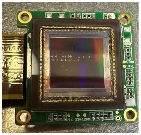
Figure 1.
FSI CMOS device.
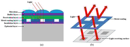
Figure 2.
(a) Cross-sectional view of the FSI CMOS; (b) schematic diagram of light incidence in the FSI CMOS.
As shown in Figure 3, a three-dimensional finite element model was developed for the CMOS structure. As shown in Figure 2b, for the FSI CMOS structure, incident light must pass through the openings in the metal routing layer to reach the photosensitive surface of the epitaxial layer, with partial light being blocked by the metal routing. Therefore, the model considered the fill factor, which is the ratio of the effective photosensitive area to the total pixel area. The experimental CMOS detector has a fill factor of approximately 70%. The model consists of 25-pixel units, each sized 5 µm × 5 µm.
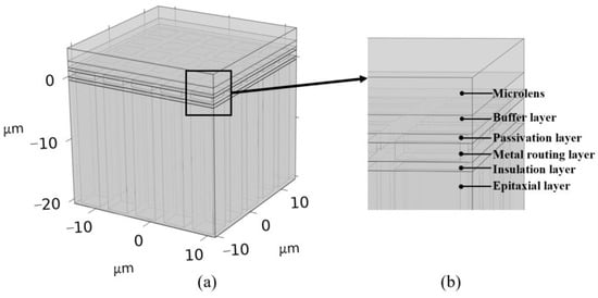
Figure 3.
(a) Schematic diagram of the CMOS 3D geometric model; (b) Enlarged schematic diagram of the layered structure in the model.
The laser irradiation process on CMOS devices involves the interaction of optical, thermal, mechanical, and electrical fields. This study focuses on analyzing thermal damage effects induced by lasers, making the following assumptions for finite element calculations: (1) Simplified to pure thermal conduction processes, ignoring non-thermal mechanisms. (2) Laser energy distribution follows a Gaussian spatial pattern. (3) Material properties remain constant with temperature variations. (4) All layers are considered continuous, isotropic media with uniform properties.
Upon reaching the CMOS surface, the laser beam’s energy is converted into a heat source with specific temporal and spatial distributions. This leads to the generation of a transient heat flow field within the CMOS multilayer structure, a process that is modeled using Fourier’s heat conduction equation [23].
where T is the instant temperature, Q is the laser heat source, , c, and k are the material density, specific heat, and heat conductivity, respectively.
When the CMOS is exposed to the nanosecond pulsed laser, the polyimide, silicon dioxide, and silicon nitride do not absorb laser heat directly. Therefore, most of the laser beam will directly illuminate the photosensitive surface of the epitaxial layer. Since silicon can absorb laser energy volumetrically, the laser heat source in this layer is considered a volumetric heat source [24]. The corresponding laser energy deposition function is expressed as follows:
Given the fill factor of the CMOS, a portion of the laser irradiates the metal routing layer. As the thickness of the metal routing layer in our model greatly surpasses its laser absorption depth (10−7–10−8 m−1), the laser heat source in this layer is classified as a surface heat source [22]. The corresponding laser energy deposition function is presented as
where represents the peak power of the laser, and the expression is
In Equations (2) and (3), is the radius of the laser spot, t represents time, corresponds to the absorption coefficient of silicon for the laser (α ≈ 7500 cm−1), R is the reflectivity of the photosensitive region in the epitaxial layer (R ≈ 0.3), is the absorptivity of aluminum to the laser (β ≈ 8%), is the single pulse energy and is the pulse width.
The temporal distribution of the pulsed laser can be expressed as follows:
The corresponding boundary conditions for convective heat exchange between the CMOS surface and ambient environment are as follows:
where h represents the convective heat transfer coefficient, is the CMOS surface temperature, and is the ambient temperature set at 298 K.
When laser irradiation begins, the initial temperature of the model is set to 298 K.
During laser irradiation, a transient and non-uniform temperature field distribution develops across CMOS layers, with spatial temperature variations inducing distinct deformation and thermal stress in each layer. This physical process can be described by the thermoelastic equilibrium equation [21,22].
Here, , , and represent the displacement components in the three orthogonal directions, while , , and are the material’s Poisson’s ratio, volumetric strain, and thermal expansion coefficient, respectively.
The stress components in three orthogonal directions are:
The stiffness matrix components C11, C12, and C13 can be determined using Young’s modulus [22].
The thermodynamic properties of the materials in each layer of the CMOS are listed in Table 1.

Table 1.
The thermodynamic parameters of materials [23].
3. Experiments
The experimental system shown in Figure 4 was used to investigate the damage characteristics. The laser source is a custom developed setup operating at a wavelength of 532 nm with a pulse width of 150 nanoseconds. The fundamental 1064 nm beam originates from a diode-pumped Nd: YAG laser module. This beam exits the laser cavity via mirrors M1 and M2. It then passes through a half-wave plate (HWP1) and a polarizing beam splitter (PBS) to produce P-polarized light. The polarized light undergoes frequency doubling to 532 nm using a half-wave plate (HWP2) and a KTP crystal. The resulting 532 nm laser beam is directed sequentially through dichroic mirror M3, energy attenuators, and a beam splitter, ultimately irradiating the CMOS target surface. Energy attenuators, including four absorptive neutral density filters and one continuous neutral density filter, were used to regulate the laser energy intensity. The beam splitter (with an approximately equal~1:1 splitting ratio) divides the laser beam into two paths. The transmitted beam irradiated the CMOS target surface, while the reflected beam was monitored by the energy meter (Ophir PE50-DIF-C) for real-time energy measurement. Output images from the CMOS detector were acquired by the computer. The experiments employed a single pulse operating in manual trigger mode. The displacement platform moved the CMOS target to unexposed areas after each pulse to avoid the thermal accumulation effect of laser energy. Damage stages were determined based on abnormal features in the CMOS output images, with corresponding laser energy density values recorded for each stage. All experiments were conducted under darkroom conditions to eliminate ambient light interference.
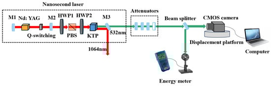
Figure 4.
Experimental system for laser-induced thermal damage in CMOS.
The 532 nm laser beam spot distribution was measured using a beam profiler (DataRay Beam’R2), as shown in Figure 5. The spot exhibits a typical Gaussian intensity distribution and its beam diameter is approximately 600 μm, with the peak intensity located at the center of the beam.
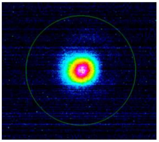
Figure 5.
Nanosecond single-pulse laser spot distribution diagram.
Based on the pulse energy measured by the energy meter and the spot size obtained from the beam profilers, the laser energy density on target was determined.
According to the law of error propagation, the relative uncertainty of a variable raised to a power is scaled by the corresponding exponent:
The relative error of the energy density is calculated as 4.24%, where δE denotes the error of the energy meter and δR represents the error of the beam spot radius.
The determination of damage stages relied on observed abnormalities in CMOS output images. As shown in Figure 6, three distinct damage stages were observed in the detector output images as the laser energy increased progressively: point damage, line damage, and complete failure. At a laser energy density of 78.9 mJ/cm2 (the single-pulse energy was measured at 0.223 mJ), an irreversible white bright spot appeared in the output image (Figure 6a), indicating localized pixel damage, and approximately 1% imaging function was lost across the device. When the energy density increased to 241.9 mJ/cm2 (the single-pulse energy was measured at 0.684 mJ), mutually perpendicular irreversible black lines emerged along both horizontal and vertical orientations in the irradiated area (Figure 6b), demonstrating full pixel failure along these linear regions while other areas maintained normal imaging function, and approximately 8% area of the device lost its imaging function at this time. Ultimately, when the energy density reached 2005.4 mJ/cm2 (the single-pulse energy was measured at 5.670 mJ), the entire sensor area failed to output any valid image (Figure 6c), marking total device failure.
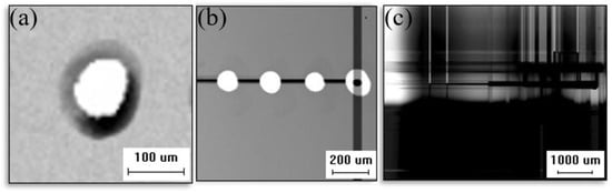
Figure 6.
Output images of CMOS at different damage stages: (a) point damage, (b) line damage, (c) complete failure.
4. Results and Analysis
4.1. Point Damage
When the laser energy density is 78.9 mJ/cm2, Figure 7 presents the optical micrograph and SEM image of the point damage. From the optical micrograph of the point-damaged area (Figure 7a), it is evident that the laser-irradiated region exhibits a typical Gaussian distribution ablation pit morphology. Additionally, SEM shows a damaged pit in the central irradiation zone (Figure 7b), exposing the disrupted epitaxial layer. Upon magnification, as shown in Figure 7c of the SEM image, it is observed that each damaged photosensitive pixel center on the epitaxial layer displays ablation, while the metal wiring between adjacent pixels remains intact. The localized melting of the epitaxial layer resulted in irreversible damage to CMOS, affecting its photoelectric conversion efficiency and charge storage performance. However, the damage was confined to the locally melted pixel areas, allowing the remaining portion to function normally for imaging purposes.
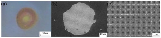
Figure 7.
Laser-induced point damage in CMOS: (a) optical micrograph, (b) SEM, (c) magnified view of SEM.
The simulated distribution of temperature and stress in the CMOS is illustrated in Figure 8a,b at the end of the irradiation period (t = 150 ns). The epitaxial layer exhibits the temperature rise and stress variation. The maximum temperature in the CMOS reaches 1750 K, located at the central point on the surface of the epitaxial layer, exceeding the melting point of silicon (1685 K). Due to the opening ratio, the temperature rise effect in the epitaxial layer is most pronounced in the areas not covered by metal wiring. The remaining heat is attributed to thermal diffusion. This scenario corresponds to the phenomenon observed in the SEM image where damaged pixels primarily experience ablation in the central region. The uneven distribution of the temperature field further leads to an uneven distribution of stress, with the maximum stress reaching 149 MPa at the interface between the insulation layer and the epitaxial layer.
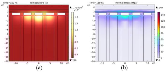
Figure 8.
Laser-induced point damage in CMOS: (a) temperature field distribution, (b) stress field distribution.
4.2. Line Damage
When the nanosecond laser’s single-pulse energy density increased to 241.9 mJ/cm2, both the area and depth of the molten region progressively expanded. The optical micrograph in Figure 9a shows the structural features of the exposed CMOS metal wiring layer due to melting. When combined with the SEM image in Figure 9b, it is evident that the area and depth of the damaged pits have significantly increased. Upon magnification in the SEM image (Figure 9c), it is observed that a considerable amount of metal wiring between pixels has undergone varying degrees of melting damage. This thermal melting damage disrupted the charge transfer pathways both horizontally and vertically between adjacent pixels, leading to the failure of the light-sensing function in the entire row of pixels. Consequently, black lines appeared both horizontally and vertically in the output image of the CMOS.
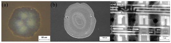
Figure 9.
Laser-induced line damage in CMOS: (a) optical micrograph, (b) SEM, (c) magnified view of SEM.
The temperature distribution and stress profile inside the detector at the end of the irradiation simulation are illustrated in Figure 10a,b. The central temperature of the laser energy deposition region significantly rises, expanding the thermal impact area within the CMOS. Consequently, the thermal damage extends to more pixel units. The maximum stress remains at the interface between the insulation layer and the epitaxial layer (peak stress of 240 MPa), with an overall increase in maximum stress values across the layers. The temperature distribution in the metal wiring layer and epitaxial layer, along with the corresponding phase transition, is depicted in Figure 10c,d. The peak temperature in the central region of the epitaxial layer reaches up to 2170 K, leading to the formation of multiple melting zones. The melting across pixels in the metal wiring layer results in a failure to enable both horizontal and vertical pixel connections.
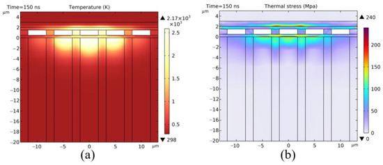
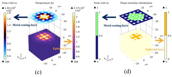
Figure 10.
Laser-induced line damage in CMOS: (a) temperature field distribution, (b) stress field distribution, (c) temperature field distribution of the metal routing layer and epitaxial layer, (d) phase transition distributions of the metal routing layer and epitaxial layer (0 and 1 in the phase transition image denote solid phase and liquid phase, respectively).
4.3. Complete Failure
When the laser energy density reaches 2005.4 mJ/cm2, as shown in Figure 11, the optical micrograph shows severe ablation pits under this energy condition, with corresponding SEM images showing distinct cracks. The CMOS multilayer structure exhibited significant protrusions due to excessive thermal expansion stress, indicating the presence of structural tearing.
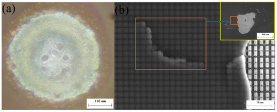
Figure 11.
Laser-induced complete failure in CMOS: (a) optical micrograph, (b) SEM.
The experimental results confirmed that the CMOS device experienced structural failure due to thermal–mechanical tearing at this stage. However, the specific damage layer responsible for complete functional failure was not clear. To investigate further, we simulated the thermal–mechanical conditions at the stage of complete failure. As shown in Figure 12a,b, the temperature of the epitaxial layer and metal routing layer increases rapidly, causing significant variations in thermal expansion stress. This leads to the formation of a stress concentration zone in the insulation layer between them. The maximum stress on the upper surface of the silicon dioxide layer reaches 502 MPa, with stress concentration at the edge regions (Figure 12c). The lower surface exhibits a peak stress of 482 MPa, decreasing radially from the center to the periphery (Figure 12d). These stress levels exceed the yield strength of silicon dioxide (300 MPa), causing the insulation layer to fracture. Subsequent crack propagation to the interface between the metal routing layer and the epitaxial layer results in interfacial delamination and additional structural damage. This thermal damage mechanism aligns with the experimentally observed tearing morphology, confirming that the thermo-mechanically induced fracture of the insulation layer was the critical factor in the complete functional failure of the CMOS device.
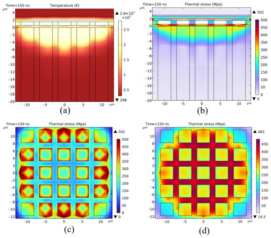
Figure 12.
Laser-induced complete failure in CMOS: (a) temperature field distribution, (b) stress field distribution, (c) stress distribution on the upper surface of the insulation layer, (d) stress distribution on the lower surface of the insulation layer.
5. Conclusions
The study investigated the thermal damage mechanisms of CMOS multilayer structures under 532 nm pulsed laser irradiation. Thermal damage in CMOS was found to be caused by thermal melting and thermal expansion stress. At a laser energy density of 78.9 mJ/cm2, localized point damage occurred in the CMOS, leading to partial pixel failure. When the energy density increased to 241.9 mJ/cm2, line damage occurred, disrupting charge transfer pathways between pixels. At a laser energy density of 2005.4 mJ/cm2, significant thermal stress led to complete structural failure of the CMOS, resulting in loss of all imaging functionality.
Author Contributions
Conceptualization, W.Z. and H.C.; methodology, W.Z. and H.C.; validation, W.Z. and H.C.; formal analysis, Y.M., X.Q. and Z.W.; investigation, Z.J.; resources, W.Z. and H.C.; data curation, Z.J., Y.M., X.Q. and Z.W.; writing—original draft preparation, Z.J. and Y.M.; writing—review and editing, W.Z. and H.C.; visualization, Z.J.; funding acquisition, W.Z. and H.C. All authors have read and agreed to the published version of the manuscript.
Funding
This research received no external funding.
Data Availability Statement
Data are contained within the article.
Acknowledgments
The authors would like to acknowledge Haixin Zhang for his assistance with the experiments.
Conflicts of Interest
The authors declare no conflicts of interest.
Abbreviations
The following abbreviations are used in this manuscript:
| CMOS | Complementary Metal-Oxide-Semiconductor |
| CCDs | Charge Coupled Devices |
| CW | Continuous-wave |
| FSI | Front-side illuminated |
| BSI | Back-side illuminated |
| SEM | Scanning electron microscopy |
References
- Bigas, M.; Cabruja, E.; Forest, J.; Salvi, J. Review of CMOS image sensors. Microelectron. J. 2006, 37, 433–451. [Google Scholar] [CrossRef]
- Gouveia, L.C.P.; Choubey, B. Advances on CMOS image sensors. Sens. Rev. 2016, 36, 231–239. [Google Scholar] [CrossRef]
- Sukhavasi, S.B.; Sukhavasi, S.B.; Elleithy, K.; Abuzneid, S.; Elleithy, A. CMOS Image Sensors in Surveillance System Applications. Sensors 2021, 21, 488. [Google Scholar] [CrossRef]
- Vala, A.; Patel, A.; Gosai, R.; Chaudharia, J.; Mewada, H.; Mahant, K. A low-cost and efficient cloud monitoring camera system design for imaging satellites. Int. J. Remote Sens. 2019, 40, 2739–2758. [Google Scholar] [CrossRef]
- Takayanagi, I.; Kuroda, R. HDR CMOS image sensors for automotive applications. IEEE Trans. Electron Devices 2022, 69, 2815–2823. [Google Scholar] [CrossRef]
- Wen, J.; Bian, J.; Li, X.; Kong, H.; Guo, L.; Lv, G. Research progress of laser dazzle and damage CMOS image sensor. Infrared Laser Eng. 2023, 52, 20230269. [Google Scholar] [CrossRef]
- Wang, A.; Guo, F.; Zhu, Z.; Xu, Z.; Cheng, X. Comparative study of hard CMOS damage irradiated by CW laser and single-pulse ns laser. High Power Laser Part. Beams 2014, 26, 091007. [Google Scholar] [CrossRef]
- Schwarz, B.; Ritt, G.; Koerber, M.; Eberle, B. Laser-induced damage threshold of camera sensors and micro-optoelectromechanical systems. Opt. Eng. 2017, 56, 034108. [Google Scholar] [CrossRef]
- Schwarz, B.; Ritt, G.; Eberle, B. Impact of threshold assessment methods in laser-induced damage measurements using the examples of CCD, CMOS, and DMD. Appl. Opt. 2021, 60, F39–F49. [Google Scholar] [CrossRef]
- Westgate, C.; James, D. Visible-Band Nanosecond Pulsed Laser Damage Thresholds of Silicon 2D Imaging Arrays. Sensors 2022, 22, 2526. [Google Scholar] [CrossRef]
- Cao, H.; Xie, X.; Chang, H.; Li, Y.; Yue, J.; Yu, Y.; Wang, Y.; Lu, Z. Laser-induced damages to charge coupled devices with combined nanosecond/picosecond short-pulse lasers. Front. Phys. 2024, 12, 1345859. [Google Scholar] [CrossRef]
- Yoon, S.; Jhang, K.Y.; Shin, W.S. Damage analysis of CMOS electro-optical imaging system by a continuous wave laser. In Proceedings of the Pacific Rim Laser Damage 2016: Optical Materials for High-Power Lasers, Yokohama, Japan, 10 August 2016. [Google Scholar] [CrossRef]
- Théberge, F.; Auclair, M.; Daigle, J.F.; Pudo, D. Damage thresholds of silicon-based cameras for in-band and out-of-band laser expositions. Appl. Opt. 2022, 61, 2473–2482. [Google Scholar] [CrossRef] [PubMed]
- Wang, X.; Zhao, N.; Zhang, Y.; Wang, B.; Dong, X.; Zou, Y.; Lei, W.; Hu, Y. Irradiation effect of 2.79 μm mid-infrared laser on CMOS image sensor. Infrared Laser Eng. 2023, 52, 20230168. [Google Scholar] [CrossRef]
- Xu, Y.; Wang, Y.; Zheng, C.; Liu, Y.; Cheng, X.; Shao, J. Experimental study on back-illuminated CMOS image sensor irradiated by CW laser. J. Appl. Opt. 2024, 45, 1072–1078. [Google Scholar] [CrossRef]
- Zhang, H.X.; Li, Y.F.; Chang, H.; Yu, Y.; Wang, G.; Wang, Y.L.; Lu, Z.W. Investigation of the damage profiles and mechanisms of CMOS devices subjected to continuous and pulsed laser exposure. Appl. Phys. B 2025, 131, 93. [Google Scholar] [CrossRef]
- Han, M.; Nie, J.; Sun, K.; Wang, X.; Dou, X.A. Experiment on the temporal evolution characteristics of a CCD multilayer structure irradiated by a 1.06 μm continuous laser. Appl. Opt. 2018, 57, 4415–4420. [Google Scholar] [CrossRef]
- Niu, C.H.; Yu, T. Damage effect evaluation of CCD irradiated by laser based on multi-source information fusion. Opt. Express 2024, 32, 18201–18215. [Google Scholar] [CrossRef]
- Dai, J.; Yu, H.; Wang, J.; Gao, X. Influence of laser energy density on thermal stress at photosensitive layer of CMOS detector. J. Appl. Opt. 2024, 45, 568–574. [Google Scholar] [CrossRef]
- Qian, F.; Peng, J.; Xu, Y. Damage mechanism of back-illuminated CMOS image sensor irradiated by pulsed laser. Chin. Opt. 2025, 18, 256–265. [Google Scholar] [CrossRef]
- Li, M.; Jin, G.; Tan, Y. Simulation of the Si-CCD irradiated by millisecond pulse laser. Optik 2017, 131, 67–71. [Google Scholar] [CrossRef]
- Ren, X.; Lei, W.; Wang, Y. Study on thermodynamic effect of CCD detector irradiated by laser. Optik 2019, 185, 497–504. [Google Scholar] [CrossRef]
- Han, M.; Wang, X.; Nie, J.; Sun, K.; Zhang, M. Temporal evolution characteristics and damage threshold of CCD detector irradiated by 1.06-μm continuous laser. Optik 2018, 157, 1282–1291. [Google Scholar] [CrossRef]
- Kou, Z.; Li, Y.; Wang, G.; Li, K.; Hou, Y.; Xie, X.; Lu, Z. Temporal evolution characteristics and mechanism analysis of CCD breakdown induced by nanosecond and picosecond pulse lasers. Optik 2022, 262, 169313. [Google Scholar] [CrossRef]
- Li, Y.; Kou, Z.; Wang, G.; Hou, Y.; Xie, X.; Yu, Y.; Wang, Y.; Lu, Z. Recent advances of short-pulse laser—Induced breakdown effect on charge-coupled device detectors. Opt. Laser Technol. 2022, 156, 108533. [Google Scholar] [CrossRef]
Disclaimer/Publisher’s Note: The statements, opinions and data contained in all publications are solely those of the individual author(s) and contributor(s) and not of MDPI and/or the editor(s). MDPI and/or the editor(s) disclaim responsibility for any injury to people or property resulting from any ideas, methods, instructions or products referred to in the content. |
© 2025 by the authors. Licensee MDPI, Basel, Switzerland. This article is an open access article distributed under the terms and conditions of the Creative Commons Attribution (CC BY) license (https://creativecommons.org/licenses/by/4.0/).