Article

Numerical Investigation of the Optimal Structure for Dynamic Plasmonic Colors Generated via Photothermal Deformation of Metal Semi-Shell Structures

1
Division of Engineering & Agriculture, Graduate School of Regional Development and Creativity, Utsunomiya University, Utsunomiya 321-8585, Japan
2
HORIBA STEC, Co., Ltd., Kyoto 601-8116, Japan
*
Author to whom correspondence should be addressed.
Photonics 2025, 12(8), 753; https://doi.org/10.3390/photonics12080753
Submission received: 26 April 2025 / Revised: 22 July 2025 / Accepted: 23 July 2025 / Published: 26 July 2025

Abstract

Nanostructure-based coloration has been investigated extensively to overcome the limitations of conventional pigments and dyes. In this study, we focused on the dynamic coloration of plasmonic structures via the photothermal deformation of a metal semi-shell. However, identifying the optimal structure using this method typically requires considerable computational time. To address the high computational cost of structural optimization in dynamic plasmonic coloration, we propose an efficient method for estimating the optimal nanostructure geometry. The color gamut area was found to be influenced by both the nanosphere density and the thickness of the metal semi-shell. The optical response of deformed semi-shells, resulting from laser-induced local heating, was simulated across a range of semi-shell shapes. From these simulations, an empirical correlation was identified that links nanoparticle diameter, density, and semi-shell thickness. This correlation enables the rapid estimation of optimal parameters, thereby reducing computational demands and supporting the efficient fabrication of dynamic plasmonic color materials.

1. Introduction

Ultraviolet light, toxicity concerns, and the challenge of coloring submicron areas pose significant obstacles in the field of coloration. Although photonic crystals and dielectric multilayers have been explored to address these problems, they face limitations, such as low reflectance and a restricted range of color variation. Metallic nanostructures are considered to be promising solutions to these challenges. For example, periodic nanodiscs and nanoholes can produce stable colors with a high spatial resolution over extended periods; however, these colors cannot be modified after fabrication. Recent advances in nanophotonics have enabled the development of structural color technologies that overcome the limitations of conventional pigmentation, offering superior tunability, resolution, and multifunctionality. A wide range of plasmonic and metamaterial-based systems have been investigated to realize dynamic, high-fidelity color control. For example, Ellenbogen et al. introduced compact plasmonic devices that integrate color filtering with polarization sensitivity, enabling tunable, durable, and high-resolution color modulation. Expanding on these multifunctional capabilities [1], Song et al. demonstrated a plasmonic polarizing metamirror capable of high-resolution color display and polarization-dependent optical encryption [2]. Xiang et al. further advanced dynamic structural coloration by employing heliconical cholesteric liquid crystals to achieve the low-voltage, real-time, and reversible tuning of reflected light across the ultraviolet to infrared spectrum [3]. Electrically tunable perfect absorbers, reported by Mirshafieyan and Gregory, offer an additional pathway toward dynamic coloration using thin, CMOS-compatible structures that combine high color fidelity with integration potential [4]. Similarly, Shu et al. employed the thermally induced phase transition of vanadium dioxide to achieve fast, reversible, and energy-efficient color switching, particularly suited for smart windows and displays [5]. Prezgot et al. proposed a lithography-free approach using thermally embedded silver nanocrystals within polymer films to fabricate scalable, low-cost, and flexible structural colors with high vibrancy and durability [6]. Duan et al. made a significant contribution by implementing subwavelength plasmonic pixels capable of energy-efficient, dynamic color tuning with long-term stability [7]. Additionally, Song et al. demonstrated a mechanically responsive structural color platform based on a stretchable substrate, enabling vivid, reversible, and angle-stable color variation without power input [8]. More recently, Geng et al. introduced a laser-based technique that combines a wide color gamut, high writing speed, ultra-high resolution, angle independence, durability, and cost-effectiveness in a streamlined inkless process [9]. Choi et al. presented a polymer-assisted photochemical deposition method that enables ambient, low-cost additive manufacturing with microscale resolution, vivid coloration, and substrate versatility [10]. Furthermore, Franklin et al. developed a self-assembled plasmonic system that provides full-color, angle-insensitive structural displays with actively addressable black states using a scalable and lithography-free fabrication process [11].
Collectively, these developments illustrate the growing versatility of dynamic structural color systems and highlight their potential for transformative applications in optical devices, high-resolution displays, security printing, and adaptive sensors.
However, they face several limitations, including the requirement for electron beam lithography, which is complicated and limited to small areas [1,7], reliance on electricity [3,4], requirement of stress and deformation [8], restricted color range [5,6], low reflectance [9,11], and requirement of complicated fabrication process [10].
The metal semi-shell structure—comprising a partial metallic shell over a dielectric core—exhibits distinct and geometrically tunable localized surface plasmon resonance (LSPR) characteristics, arising from its inherent asymmetry and hybrid dielectric–metal configuration. The LSPR wavelength is highly sensitive to structural parameters such as semi-shell thickness, capping angle (e.g., hemispherical or crescent-shaped), core diameter, and refractive index [12]. This tunability enables precise control over both the resonance peak position and spectral linewidth, thereby facilitating applications in color tuning and plasmonic sensing. Such LSPR behavior is particularly advantageous for the generation of vivid and spectrally pure structural colors.
Previous studies have demonstrated that dynamic plasmonic coloring utilizing a metal semi-shell structure facilitates the efficient and cost-effective processing of large areas and exhibits the potential to achieve a broad color gamut [13]. In this study, the reflection spectra were computed using the discrete dipole approximation (DDA) for various diameters and densities of the nanospheres, thicknesses of the metal semi-shells, and shapes of the capping angles of the metal semi-shells. The color gamut area was defined as the polygonal region on the chromaticity diagram delineated by multiple coordinates derived from the reflection spectra. The color gamut area is influenced by both the density of the nanospheres and the thickness of the semi-shell. Before depositing the semi-shell, the thickness that maximizes the color gamut area, which depends on the density of the nanospheres, must be estimated. The chromaticity coordinates were determined via time-consuming DDA calculations performed for each combination of the nanosphere diameter, density, semi-shell thickness, and capping angle of the semi-shell. For example, calculations for a nanosphere with diameters, densities, semi-shell thicknesses, and capping angles of 100 nm, 19.8 µm−2, 20 nm, and 90°, respectively, required 23 h and 25 min when using DDSCAT7.3.3 [14] software on a self-assembled PC equipped with an Intel Core i7-8700 3.2 GHz processor. To reduce the computational time, estimating the semi-shell thickness that optimizes the color gamut area for specific values of nanosphere diameter and density is advantageous.
This study demonstrates that the semi-shell thickness that maximizes the color gamut area for a given nanosphere diameter and density is strongly correlated with both the diameter and density.

2. Materials and Methods

The calculations included the incident angle, polarization, wavelength, nanostructure material and shape, chromaticity coordinates, and the evaluation index by area on a chromaticity diagram. The metal semi-shell structures considered in this study are typically fabricated by immersing a substrate in a liquid containing dispersed nanospheres, which allows the nanospheres to adhere to the substrate and subsequently deposit metal onto them.
It is well established that the particle size of silica nanospheres significantly influences their aggregation behavior during substrate deposition. Nanoparticles with diameters below 30 nm tend to aggregate due to high surface energy and incomplete surface modification, even when silane coupling agents are used [15]. On the other hand, particles around 200 nm can also exhibit aggregation during drying or settling due to gravitational sedimentation and capillary forces [16]. Therefore, appropriate size selection and process control are essential to ensure uniform deposition without aggregation.

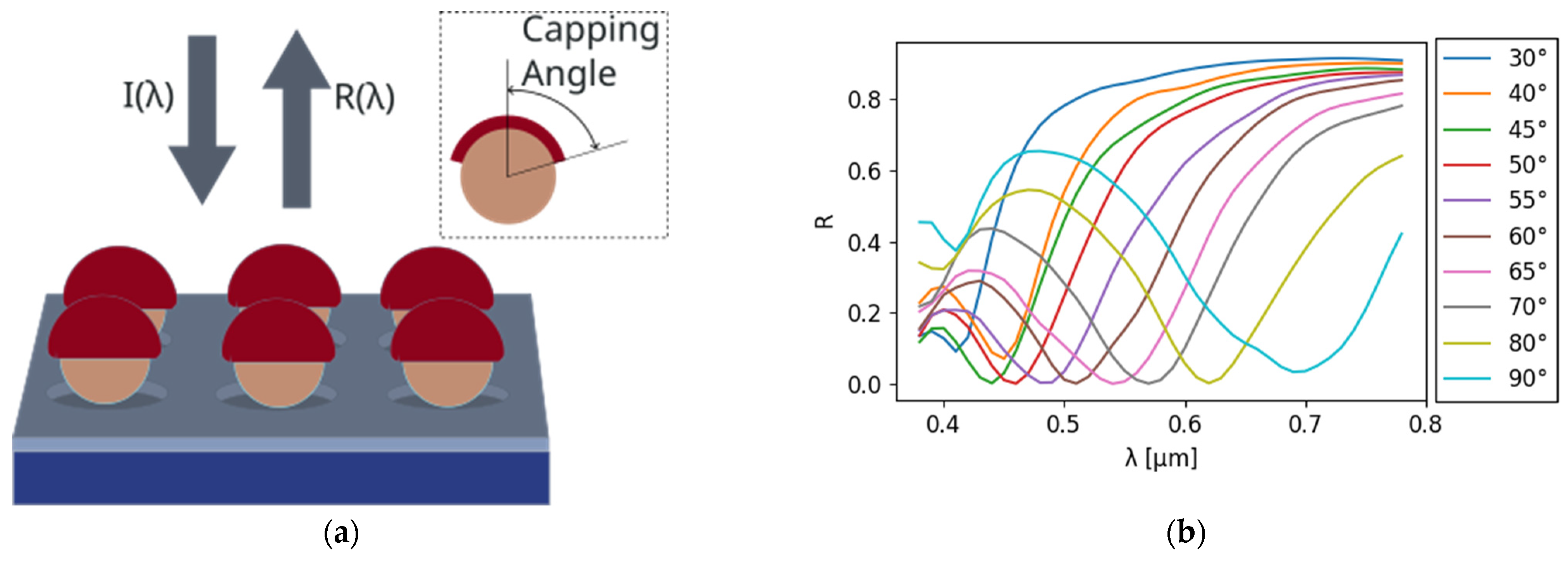
2.1. Materials and Structure

The core material was fused silica, which was chosen because of its heat resistance and widespread availability. Aluminum was selected as the substrate material because of its cost-effectiveness and widespread availability. Silver was used as the deposition material to achieve the broadest color gamut, as demonstrated in previous studies [13]. The refractive indices of fused silica, aluminum, and silver were obtained from the literature [17,18,19]. The diameters of the nanospheres were 50, 75, and 100 nm, and the substrate thickness was 40 nm. The deposition thicknesses and densities are listed in Table 1. The capping angles of the semi-shells varied by 30°, 40°, 45°, 50°, 55°, 60°, 65°, 70°, 80°, and 90°.

2.2. Reflectance Spectrum

Figure 1a illustrates the reflection of incident light from a nanostructure composed of a substrate, nanospheres, and a metal semi-shell. The deformation of the semi-shell owing to laser-induced local heating was simulated at various irradiation intensities. Upon laser irradiation, the metal semi-shell underwent local heating, leading to melting and deformation driven by surface tension [12], photothermophoretic force [20], and optical force [21]. In the present study, the shape proposed by Asato et al. [22] was adopted as the model geometry for simulations using the DDA method. The capping angle varied from 90° to 30°. The reflectance spectra were calculated using the DDA method with the DDSCAT 7.3.3 software [14]. The wavelength varied from 380 to 780 nm in increments of 10 nm. The refractive index of the surrounding medium was set as 1.0, and two orthogonal incident polarizations, each at an incidence angle of 0°, were applied to the nanostructures. The target geometry consisted of a unit nanostructure periodically repeated in two dimensions, and periodic boundary conditions were applied in both in-plane directions to model an infinite two-dimensional array. The resulting reflection spectra are shown in Figure 1b.

2.3. Calculation Condition

For the DDA calculations, a dipole spacing of 2 nm was adopted. Although the use of a finer spacing (1 nm) resulted in a slight shift (~10 nm) in the reflectance trough and caused a less than 10% change in the enclosed area on the chromaticity diagram, it increased the total number of dipoles by approximately a factor of eight. Considering this substantial increase in computational cost and the relatively minor impact on the spectral and chromaticity results, a 2 nm spacing was deemed a reasonable compromise between accuracy and efficiency. The densities of the nanostructures and the number of dipoles are listed in Table 1. Because the nanoparticles were placed closer to the substrate than to their neighboring nanoparticles, the plasmon coupling between the nanoparticles and the substrate was stronger than that between the nanoparticles themselves [23]. Consequently, the absorption characteristics of the periodic structure closely resembled those of a random structure. The error tolerance was 10−4.

2.4. Color Gamut Area in Commission Internationale De L’éclairage (CIE) Luv Color Space

The tristimulus values, XYZ, of the light were calculated from the reflectance spectrum R(λ) at each capping angle, the CIE standard light source D65 spectrum I(λ), and the isochromatic function of the CIE 1931, a 2° colorimetric standard observer [24,25], which represents the average human color perception over a 2° visual field, as expressed by Equation (1) as follows:
X Y Z = 1 k λ x ¯ λ y ¯ λ x ¯ ` λ I λ R λ d λ k = λ y ¯ λ I λ d λ .
In Equation (1), x ¯ λ ,   y ¯ λ , and z ¯ ( λ ) are the CIE 1931 color-matching functions of a 2° observer (Figure 1c) [26]. The values in the CIE XYZ color space were then converted to the CIE Luv color space (Figure 1d), as follows [27]:
u = 4 X X + 15 Y + 3 Z v = 9 Y X + 15 Y + 3 Z .
The area S enclosed by the coordinate points derived from the reflectance spectra of all capping angles in the CIE Luv color space, calculated using Equation (3), was adopted as the evaluation criterion [28].
S = 1 2 u j u j + 1 v j + v j + 1

3. Results

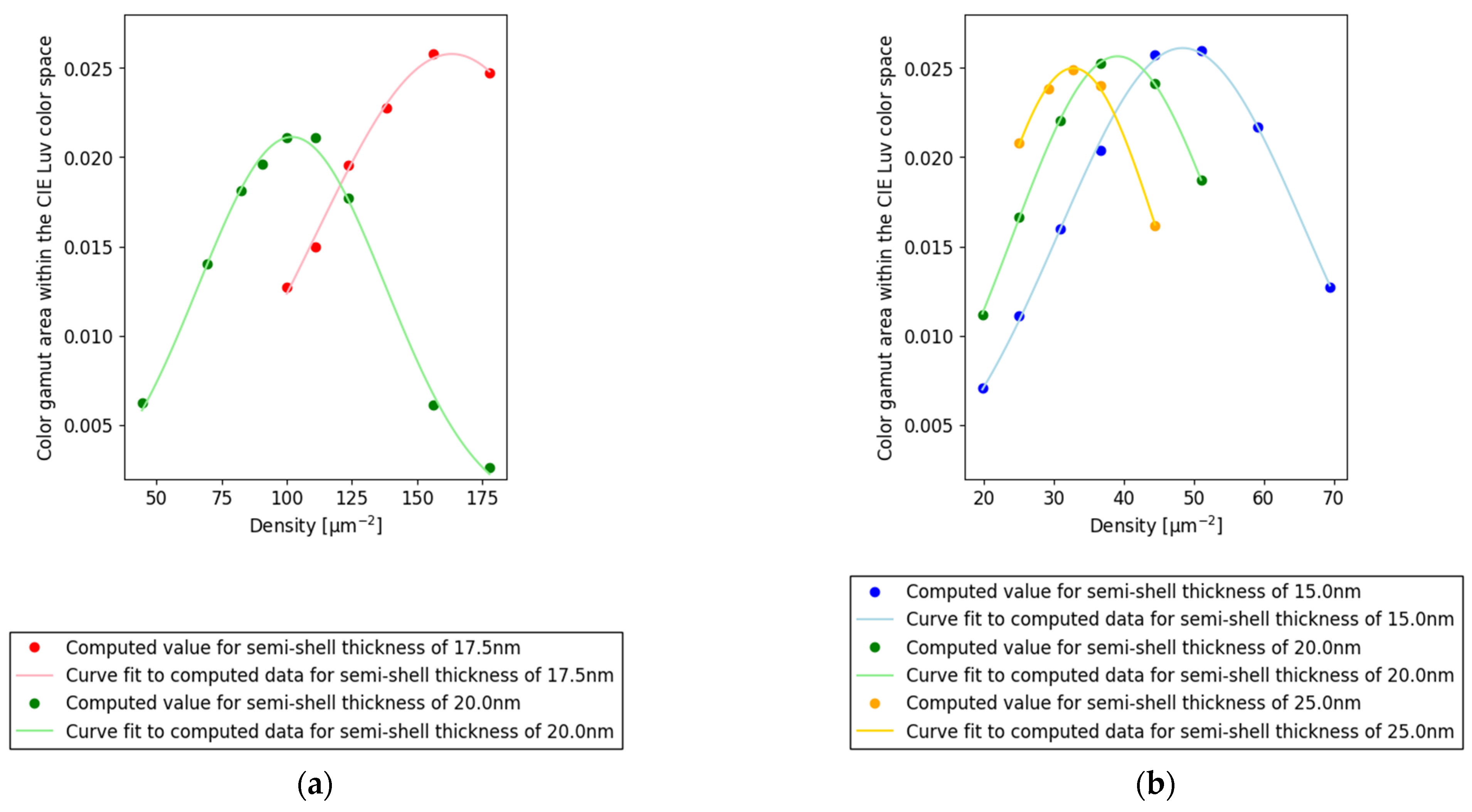
3.1. Color Gamut Areas in the CIE Luv Chromaticity Diagram

Figure 2a–c show the color gamut areas in the CIE Luv chromaticity diagrams. The x-axis represents the density, whereas the y-axis depicts the color gamut area within the CIE Luv color space. For each nanosphere diameter and semi-shell thickness, the color gamut area was maximized at a specific density.

3.2. Density of the Maximum Color Gamut Area for Each Core Diameter and Semi-Shell Thickness

The color gamut area corresponding to each nanosphere and semi-shell thickness was fitted using a Gaussian function. The central values of the resulting Gaussian functions are listed in Table 2. This central value was identified as the point at which the color gamut area reached its maximum value. These data points were approximated using the equation for a plane (4) as follows:
z = a x + b y + c .
The following coefficients and determination coefficient were obtained as follows:
a = 0.6058 , b = 0.2283 , c = 28.91 , R 2 = 0.9289 .
The data were sufficiently approximated by a plane, as illustrated in Figure 2d.

4. Discussion

4.1. Validation of the Approximation Formula

In the case of a core diameter of 75 nm and density of 45.0 µm−2, which corresponds to a center-to-center distance of 149.0 nm, the maximum color gamut area obtained using the approximate Formula (4) was 17.5 nm in semi-shell thickness. Figure 3a illustrates the calculated color gamut area for a core diameter of 75 nm and a semi-shell thickness of 17.5 nm. Additionally, the figure demonstrates that the densities at which the color gamut area reached its peak are almost identical. Moreover, as summarized in Table 3 and illustrated in Figure 3b, point (75, 149.0, 17.5) lies closer to the fitted plane than the data points used to construct the plane. This proximity confirms the validity of the estimation.

4.2. Structure That Maximizes the Color Gamut Area

To expand the color gamut area, the reflectance trough values appearing at each capping angle must be as close as possible to zero. For example, Figure 3c shows the reflectance spectra at each capping angle for a core diameter of 75 nm, semi-shell thickness of 20 nm, and center-to-center distance of 140 nm. At a capping angle of 70°, a reflectance trough appears at a wavelength of 0.58 µm. Figure 3d shows the relationship between the center-to-center distance and the absorption for a core diameter of 75 nm, semi-shell thickness of 20 nm, and capping angle of 70°. When the center-to-center distance between nanostructures was within the range of 140–165 nm, the absorption peak decreased due to enhanced plasmonic coupling. This coupling induced spectral broadening [29], reducing the peak intensity and thereby decreasing the enclosed area in the chromaticity diagram. As the interparticle distance increased beyond 165 nm, the spectral broadening effect diminished and the absorption peak became sharper. However, the overall absorption was still reduced because the lower density of nanostructures resulted in a relatively greater contribution from substrate reflection. In both regimes—below and above 165 nm—the deviation from the optimal distance led to a shift in the reflectance minimum away from zero, which in turn shifted the chromaticity coordinates closer to white and decreased the color gamut area.

5. Conclusions

In this study, we propose a method for estimating the optimum thickness of metal deposition to expand the color gamut of plasmonic colors generated by nanostructures. These nanostructures were fabricated by dipping a substrate in a liquid containing dispersed nanospheres, followed by metal deposition to form semi-shell structures. The resulting color gamut area was found to be influenced by both the density of the nanospheres and the thickness of the semi-shell. The deformation of the semi-shell owing to laser-induced local heating was simulated to evaluate semi-shell deformation under various irradiation intensities. The results indicated that the semi-shell thickness that maximized the color gamut area for a given nanosphere diameter and density was strongly correlated with both the diameter and density. To reduce computational effort, an estimation method was developed to predict the optimal semi-shell thickness for specific nanosphere configurations, enabling the more efficient fabrication of dynamically tunable plasmonic color materials. The proposed estimation method enables the direct prediction of the optimal semi-shell thickness, significantly reducing computational cost. Conventionally, determining the optimal thickness requires simulations under at least three different conditions, each taking approximately 23.5 h, as stated in the Introduction. By eliminating the need for such exhaustive computations, the method facilitates the more efficient design of dynamically tunable plasmonic color materials.
However, a fundamental limitation of photothermal plasmonic coloration is the typically single-peaked nature of the plasmonic absorption spectrum, which restricts the attainable color gamut—particularly in the green region, where more complex spectral shaping is required to achieve high color purity. To address this issue, recent studies have explored strategies such as the introduction of multiple resonant modes through complex nanostructure geometries [2], the use of hybrid metal–dielectric multilayer designs [30], and the implementation of reconfigurable plasmonic architectures [31]. These approaches provide broader spectral control and offer promising directions for overcoming the intrinsic limitations of single-mode plasmonic systems. Building on the present approach, a promising direction for future work is its application to metal semi-shell structures, where geometrical tunability and plasmonic resonance behavior are more complex. Extending the estimation framework to such architectures may enable a more comprehensive optimization of color gamut characteristics in dynamically reconfigurable plasmonic systems.

Author Contributions

Conceptualization, R.F. and M.M.; Data curation, M.M.; Formal analysis, R.F. and M.M.; Funding acquisition, M.M.; Investigation, M.M.; Methodology, R.F. and M.M.; Project, R.F. and M.M.; Resources, R.F. and M.M.; Software, R.F. and M.M.; Supervision, R.F.; Validation, R.F. and M.M.; Visualization, M.M.; Writing—original draft, M.M.; Writing—review and editing, R.F. and M.M. All authors have read and agreed to the published version of the manuscript.

Funding

This research received no external funding.

Data Availability Statement

The raw data supporting the conclusions of this article will be made available by the authors on request.

Conflicts of Interest

Author Masaaki Magari is employed by the company HORIBA STEC Co., Ltd. The remaining author declares that the research was conducted in the absence of any commercial or financial relationships that could be construed as a potential conflict of interest.

References

  1. Ellenbogen, T.; Seo, K.; Crozier, K.B. Chromatic plasmonic polarizers for active visible color filtering and polarimetry. Nano Lett. 2012, 12, 1026–1031. [Google Scholar] [CrossRef]
  2. Song, M.; Li, X.; Pu, M.; Guo, Y.; Liu, K.; Yu, H.; Ma, X.; Luo, X. Color display and encryption with a plasmonic polarizing metamirror. Nanophotonics 2018, 7, 323–331. [Google Scholar] [CrossRef]
  3. Xiang, J.; Li, Y.; Li, Q.; Paterson, D.A.; Storey, J.M.-D.; Imrie, C.T.; Lavrentovich, O.D. Electrically tunable selective reflection of light from ultraviolet to visible and infrared by heliconical cholesterics. Adv. Mater. 2015, 27, 3014–3018. [Google Scholar] [CrossRef]
  4. Mirshafieyan, S.S.; Gregory, D.A. Electrically tunable perfect light absorbers as color filters and modulators. Sci. Rep. 2018, 8, 2635. [Google Scholar] [CrossRef]
  5. Shu, F.-Z.; Yu, F.-F.; Peng, R.-W.; Zhu, Y.-Y.; Xiong, B.; Fan, R.-H.; Wang, Z.-H.; Liu, Y.; Wang, M. Dynamic plasmonic color generation based on phase transition of vanadium dioxide. Adv. Opt. Mater. 2018, 6, 1700939. [Google Scholar] [CrossRef]
  6. Prezgot, D.; Tatarchuk, S.W.; Ianoul, A. Plasmonic color generation in silver nanocrystal-over-mirror films by thermal embedment into a polymer spacer. Nano Sel. 2022, 3, 1082–1090. [Google Scholar] [CrossRef]
  7. Duan, X.; Kamin, S.; Liu, N. Dynamic plasmonic colour display. Nat. Commun. 2017, 8, 14606. [Google Scholar] [CrossRef]
  8. Song, S.C.; Ma, X.L.; Pu, M.B.; Li, X.; Liu, K.P.; Gao, P.; Zhao, Z.Y.; Wang, Y.Q.; Wang, C.T.; Luo, X.G. Actively tunable structural color rendering with tensile substrate. Adv. Opt. Mater. 2017, 5, 1600829. [Google Scholar] [CrossRef]
  9. Geng, J.; Xu, L.; Yan, W.; Shi, L.; Qiu, M. High-speed laser writing of structural colors for full-color inkless printing. Nat. Commun. 2023, 14, 565. [Google Scholar] [CrossRef]
  10. Choi, S.; Zhao, Z.; Zuo, J.; Faruque, H.M.R.; Yao, Y.; Wang, C. Structural color printing via polymer-assisted photochemical deposition. Light. Sci. Appl. 2022, 11, 84. [Google Scholar] [CrossRef]
  11. Franklin, D.; He, Z.; Mastranzo Ortega, P.; Safaei, A.; Cencillo-Abad, P.; Wu, S.; Chanda, D. Self-assembled plasmonics for angle-independent structural color displays with actively addressed black states. Proc. Natl. Acad. Sci. USA 2020, 117, 13350–13358. [Google Scholar] [CrossRef]
  12. Fujimura, R.; Zhang, R.; Kitamoto, Y.; Shimojo, M.; Kajikawa, K. Modeling of semi-shell nanostructures formed by metal deposition on dielectric nanospheres and numerical evaluation of plasmonic properties. Jpn. J. Appl. Phys. 2014, 53, 035201. [Google Scholar] [CrossRef]
  13. Magari, M.; Fujimura, R. Numerical investigation of dynamic plasmonic color generated via photothermal deformation of a metal semi-shell structure. Jpn. J. Appl. Phys 2024, 63, 082001. [Google Scholar] [CrossRef]
  14. Draine, B.T.; Flatau, J. Discrete-dipole approximation for scattering calculations. J. Opt. Soc. Am. A 1994, 11, 1491–1499. [Google Scholar] [CrossRef]
  15. Fujimoto, K.; Nagao, D.; Konno, M. Effect of particle size on surface modification of silica nanoparticles with hexyltrimethoxysilane (C6S) and its influence on the dispersion stability of silica particles in methylethylketone (MEK). J. Colloid Interface Sci. 2007, 309, 394–401. [Google Scholar]
  16. Bigioni, T.P.; Lin, X.M.; Nguyen, T.T.; Corwin, E.I.; Witten, T.A.; Jaeger, H.M. Kinetically driven self-assembly of highly ordered nanoparticle monolayers. Nat. Mater. 2006, 5, 265–270. [Google Scholar] [CrossRef]
  17. Malitson, I.H. Interspecimen comparison of the refractive index of fused silica. J. Opt. Soc. Am. 1965, 55, 1205–1209. [Google Scholar] [CrossRef]
  18. Polyanskiy, M.N. Refractiveindex.info database of optical constants. Sci. Data 2024, 11, 94. [Google Scholar] [CrossRef]
  19. Rakic, A.D.; Djurisic, A.B.; Elazar, J.M.; Majewski, M.L. Optical properties of metallic films for vertical-cavity optoelectronic devices. Appl. Opt. 1998, 37, 5271–5283. [Google Scholar] [CrossRef]
  20. Wang, S.; Ding, T. Photothermal-Assisted Optical Stretching of Gold Nanoparticles. ACS Nano 2019, 13, 32–37. [Google Scholar] [CrossRef]
  21. Yao, J.; Li, Y.; Wang, S.; Ding, T. Thin-Film-Assisted Photothermal Deformation of Gold Nanoparticles. A Facile and In-Situ Strategy for Single-Plate-Based Devices. ACS Nano 2024, 18, 10618–10624. [Google Scholar] [CrossRef]
  22. Asato, N.; Fujimura, R. Tunable plasmonic resonance by photothermal deformation in Ag-SiO2 semi-shell nanostructure and enlargement of the controllable spectral region by UV-curable resin. Opt. Rev. 2024, 31, 488–495. [Google Scholar] [CrossRef]
  23. Chevalier, P.; Bouchon, P.; Jaeck, J.; Lauwick, D.; Bardou, N.; Kattnig, A.; Pardo, F.; Haïdar, R. Absorbing metasurface created by diffractionless disordered arrays of nanoantennas. Appl. Phys. Lett. 2015, 107, 251108. [Google Scholar] [CrossRef]
  24. Smith, T.; Guild, J. The CIE colorimetric standards and their use. Trans. Opt. Soc. 1931, 33, 73. [Google Scholar] [CrossRef]
  25. Ohta, N.; Robertson, A.R. CIE Standard Colorimetric System. In Colorimetry; Kriss, M.A., Lowe, A.C., MacDonald, L.W., Miyake, Y., Eds.; Wiley: Chichester, UK, 2005. [Google Scholar]
  26. CIE. CIE 1931 Colour-Matching Functions, 2 Degree Observer (Data Table); International Commission on Illumination (CIE): Vienna, Austria, 2018. [Google Scholar]
  27. Carter, E.C.; Schanda, J.D.; Hirschler, R.; Jost, S.; Luo, M.R.; Melgosa, M.; Ohno, Y.; Pointer, M.R.; Rich, D.C.; Viénot, F.; et al. CIE 015:2018 Colorimetry, 4th ed.; Commission Internationale de l’Eclairage: Vienna, Austria, 2018. [Google Scholar]
  28. Braden, B. The surveyor’s area formula. College Math. J. 1986, 17, 326–337. [Google Scholar] [CrossRef]
  29. Jain, P.K.; Huang, W.; El-Sayed, M.A. On the universal scaling behavior of the distance decay of plasmon coupling in metal nanoparticle pairs: A plasmon ruler equation. Nano Lett. 2007, 7, 2080–2088. [Google Scholar] [CrossRef]
  30. Chen, W.T.; Yang, K.Y.; Wang, C.M.; Huang, Y.W.; Sun, G.; Chiang, I.D.; Liao, C.Y.; Hsu, W.L.; Lin, H.T.; Sun, S.; et al. High-efficiency broadband meta-hologram with polarization-controlled dual images. Nat. Commun. 2014, 5, 4802. [Google Scholar] [CrossRef]
  31. Yoon, G.; Kim, K.; Huh, D.; Rho, J. Single-step manufacturing of hierarchical dielectric metalens in the visible. Nat. Commun. 2020, 11, 2268. [Google Scholar] [CrossRef]
Figure 1. (a) Schematic of reflection of incident light from the structure. Inset: capping angle. (b) Reflectance spectra corresponding to a diameter of 75 nm, semi-shell thickness of 20 nm, and a center-to-center distance of 165 nm. (c) CIE1931 color matching functions of a 2° observer. (d) Change in the color gamut of Ag semi-shells of 20 nm thickness on silica cores of 75 nm on Al substrate at a density of 36.7 μm−2 as the capping angle decreases from 90° to 30° in the CIE Luv chromaticity diagram. The background shows the estimated visible colors corresponding to each chromaticity coordinate (u′, v′). Due to limitations of display devices and color gamut mapping, the shown colors are only illustrative approximations.
Photonics 12 00753 g001aPhotonics 12 00753 g001b
Figure 2. Color gamut areas in CIE Luv color space for (a) core diameter of 50 nm and semi-shell thicknesses of 17.5 nm and 20 nm; (b) core diameter of 75 nm and semi-shell thicknesses of 15, 20, and 25 nm; (c) core diameter of 100 nm and semi-shell thicknesses of 15, 20, and 25 nm. (d) Core diameter, period, and thickness difference. X-axis: core diameter [nm], y-axis: period [nm], and z-axis: semi-shell thickness difference from the approximated plane [nm].
Photonics 12 00753 g002aPhotonics 12 00753 g002b
Figure 3. (a) Color gamut area in the CIE Luv color space for a core diameter of 75 nm and a semi-shell thickness of 17.5 nm. (b) Semi-shell thickness difference in the predicted data from the approximated plane. (c) Reflectance spectra at core diameter of 75 nm, semi-shell thickness of 20 nm, and center-to-center distance of 140 nm. The trough of the reflectance spectrum at a wavelength of 0.58 µm at a capping angle of 70° has a reflectance of approximately 0.1. (d) Absorption at a wavelength of 0.58 µm for a core diameter of 75 nm and semi-shell thickness of 20 nm at a capping angle of 70°. (e) Absorption spectra of different center-to-center distances for a core diameter of 75 nm and semi-shell thickness of 20 nm at a capping angle of 70°.
Photonics 12 00753 g003
Table 1. Representative conditions used in the dipole calculation for different nanostructure sizes.
Diameter of Nanosphere [nm]Density
[µm−2]
Deposition Thickness
[nm]
Average Number of Dipoles of All the Capping Angles
50177.78 17.550,363.1
50100.00 17.582,043.1
50177.78 2050,000.1
5044.44 20184,503.2
7559.17 15156,010.5
7519.75 15401,388.5
7551.02 20177,278.0
7519.75 20428,254.0
7544.44 25218,923.2
7525.00 25362,539.2
10027.99 15327,747.8
10016.00 15520,887.8
10032.65 20302,464.7
10011.11 20759,900.7
10025.00 25400,139.9
10013.22 25707,635.9
Table 2. Best density for each nanostructure.
Core Diameter
[nm]
Semi-Shell Thickness [nm]Density
[µm−2]
Center-to-Center Distance [nm]
5017.5163.325±2.06478.2
5020101.986±0.66399.0
751548.396±0.173143.7
752039.089±0.048159.9
752532.759±0.160174.7
1001524.141±0.053203.5
1002019.734±0.198225.1
1002515.838±0.052251.3
Table 3. Difference between semi-shell thickness and the approximated semi-shell thickness.
Core Diameter
[nm]
Semi-Shell Thickness [nm]
(a)
Center-to-Center Distance [nm]Approximated Semi-Shell Thickness [nm]
(b)
Difference Between Semi-Shell Thickness and the Approximated Semi-Shell Thickness [nm] (a)–(b)
A5017.578.216.4731.027
502099.021.222−1.222
7515143.716.282−1.282
7520159.919.9800.020
7525174.723.3591.641
10015203.514.7890.211
10020225.119.7200.280
10025251.325.702−0.702
B7517.5149.017.4920.008
Note: A was used to calculate the plane and B was used for validation.
Disclaimer/Publisher’s Note: The statements, opinions and data contained in all publications are solely those of the individual author(s) and contributor(s) and not of MDPI and/or the editor(s). MDPI and/or the editor(s) disclaim responsibility for any injury to people or property resulting from any ideas, methods, instructions or products referred to in the content.

