Article

Superlattice Structure for High Performance AlGaN Deep Ultraviolet LEDs

by
Mano Bala Sankar Muthu
,
Ravi Teja Velpula
,
Barsha Jain
and
Hieu Pham Trung Nguyen
*
Department of Electrical and Computer Engineering, Texas Tech University, 910 Boston Avenue, Lubbock, TX 79409, USA
*
Author to whom correspondence should be addressed.
Photonics 2025, 12(8), 752; https://doi.org/10.3390/photonics12080752
Submission received: 1 July 2025 / Revised: 22 July 2025 / Accepted: 24 July 2025 / Published: 26 July 2025
(This article belongs to the Section Optoelectronics and Optical Materials)

Abstract

This study presents a novel approach to mitigate electron overflow in deep ultraviolet (UV) AlGaN light-emitting diodes (LEDs) by integrating engineered quantum barriers (QBs) with a concave shape and an optimized AlGaN superlattice (SL) electron blocking layer (EBL). The concave QBs reduce electron leakage by lowering the electron thermal velocity and mean free path, enhancing electron capture in the active region. The SL EBL further reduces electron overflow without compromising hole transport. At a wavelength of ~253.7 nm, the proposed LED demonstrates a 2.67× improvement in internal quantum efficiency (IQE) and a 2.64× increase in output power at 150 mA injection, with electron leakage reduced by ~4 orders of magnitude compared to conventional LEDs. The efficiency droop is found to be just 2.32%.

1. Introduction

AlGaN-based devices have undergone accelerated technological evolution and substantial advancements in performance over the past two decades due to their superior optical properties and efficiency [1,2,3,4]. Moreover, AlGaN deep ultraviolet (UV) LEDs are being explored as a viable alternative to mercury lamps [5,6], offering advantages such as compact size, long operational lifetime, low power consumption, and tunable optical emission, further making them suitable for applications in sterilization [7], data preservation, water purification [8], and advanced biomedical research [9,10,11,12,13]. Despite their potential applications, the efficiency and output power of AlGaN deep-UV LEDs remain limited, primarily due to factors such as significant defects and dislocations from lattice mismatch in epilayers, polarization-induced quantum-confined Stark effect (QCSE), and electron leakage, along with insufficient hole injection efficiency [14,15,16].
Extensive research has been conducted to address the electron leakage problem [15] with various device engineering designs in the active region, including staggered quantum wells (QWs) [17], intrinsic strip-in-a-barrier structures [18], and many others [19,20]. Further, electron leakage has been suppressed by introducing a p-doped and high-Al composition bulk electron blocking layer (EBL) after the active region, leveraging its enhanced bandgap to suppress electron leakage and improve carrier confinement [21]. Next, EBL is optimized with graded layers [22,23], polarization-modulated regions, and superlattice structures [24,25,26,27] to better control electron overflow from the active region. Overall, these device optimizations in the active region and EBL have demonstrated partial suppression of electron leakage from the active region but not completely.
In this context, this paper introduces a novel technique to reduce electron overflow in AlGaN deep UV LEDs by employing concave quantum barriers (QBs) in conjunction with an optimized AlGaN superlattice (SL) electron blocking layer (EBL). The concave QBs effectively suppress electron leakage by reducing the electron thermal velocity and mean free path (MFP), thereby increasing electron capture efficiency within the active region. Meanwhile, the SL EBL mitigates the remaining electron overflow while maintaining effective hole transport at a wavelength of approximately 253.7 nm. The proposed LED structure is anticipated to substantially optimize internal quantum efficiency (IQE), output power, and radiative recombination rates, driven by advanced engineering of carrier dynamics and material interfaces.

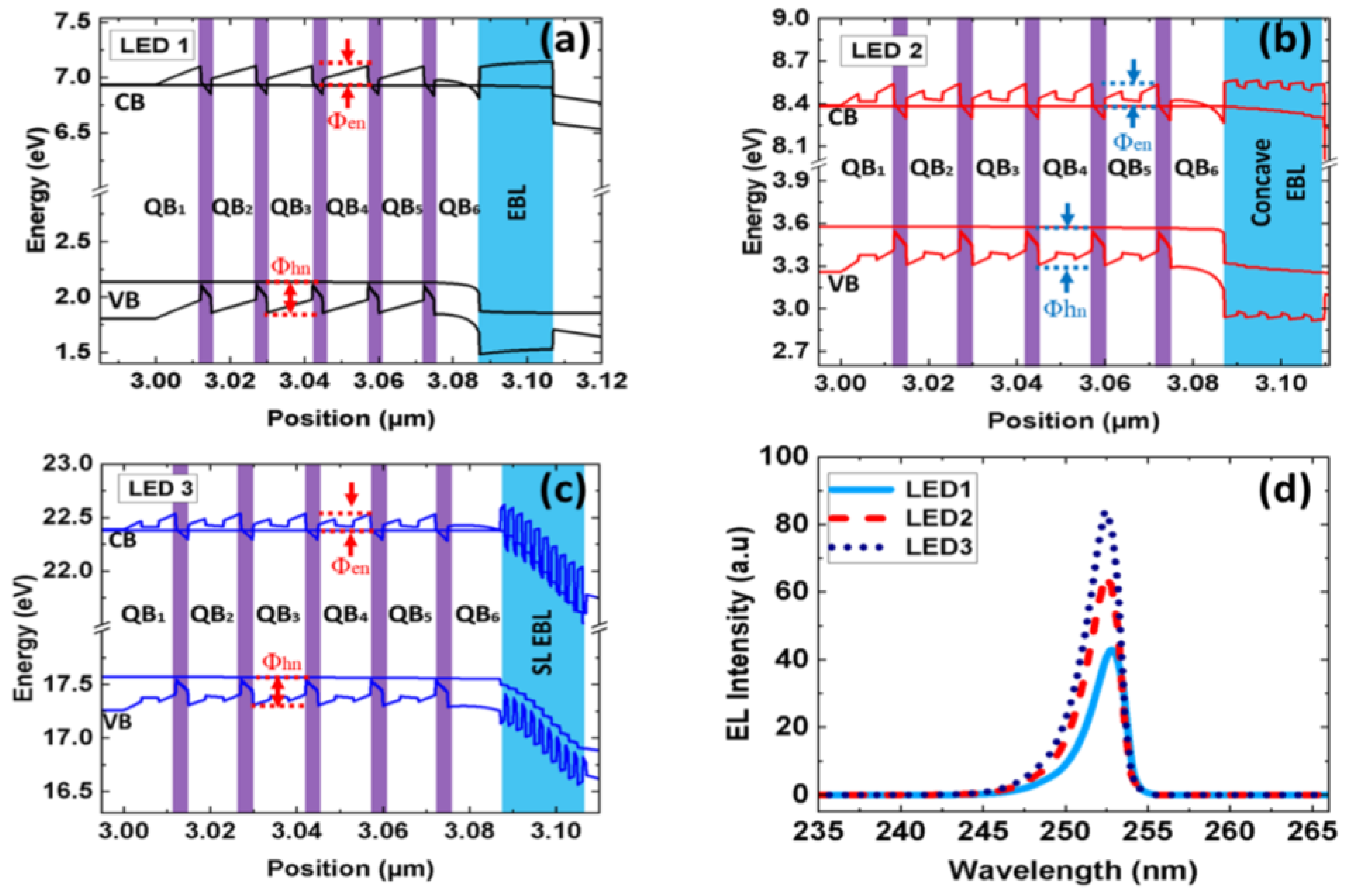
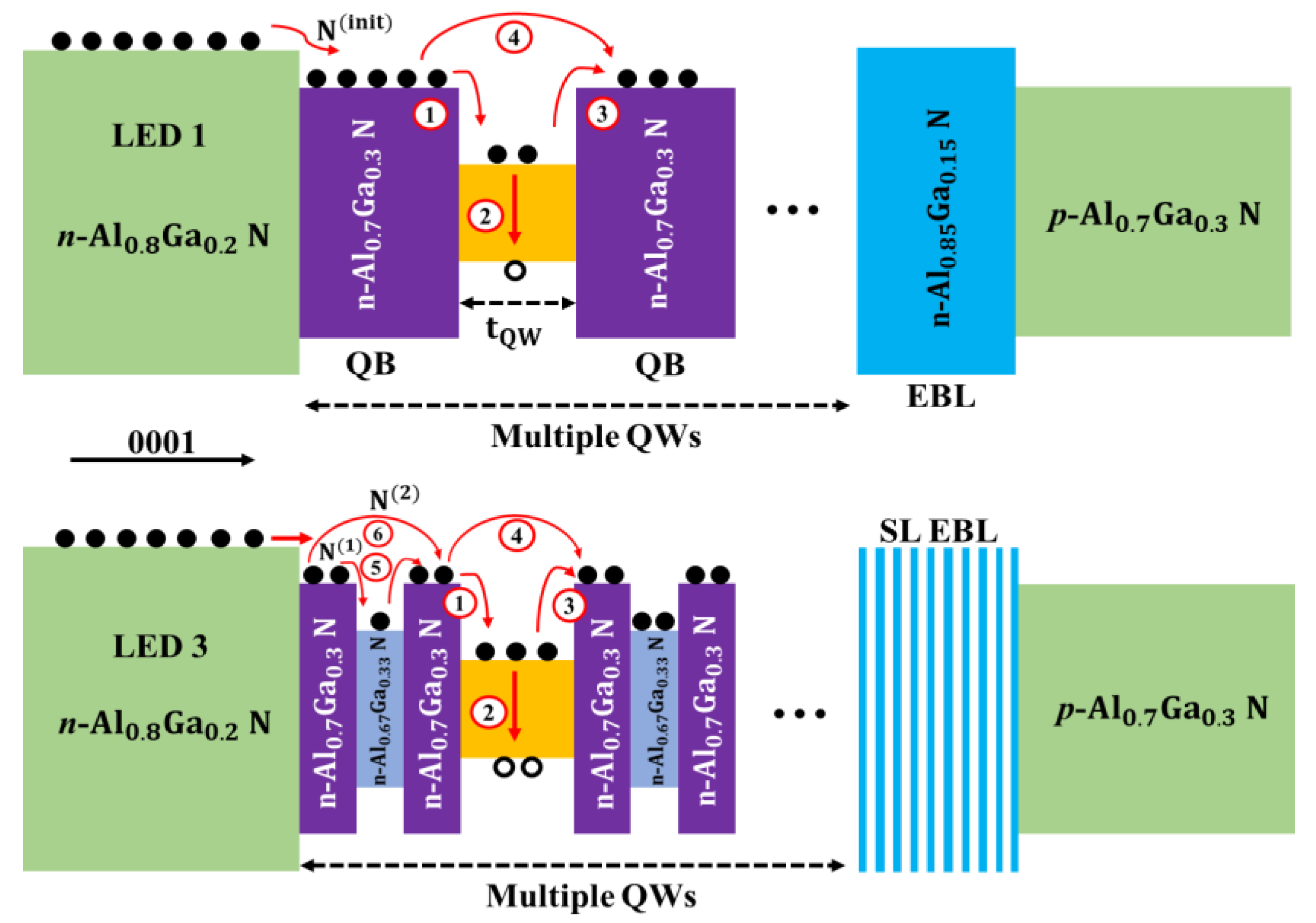
2. Device Structure and Parameters

The AlGaN Deep UV LED structure used for reference is based on the LED fabricated by Yan et al. [28]. Figure 1a shows a schematic representation of the conventional LED structure, i.e., LED1. Next, conduction band schematics, along with the Al composition regarding the EBL for LED1, LED2, and LED3, are shown in Figure 1b. The Al composition (%) profile of the active region and EBL for all LEDs is shown in Figure 1c. The LED1 contains a 3 μm n-Al0.8Ga0.2N layer (doping concentration: 5 × 1024 cm−3), five undoped 3 nm Al0.6Ga0.4N QWs sandwiched between six undoped 12 nm Al0.7Ga0.3N QBs as an active region, a 20 nm p-Al0.85Ga0.15N (doping concentration: 3 × 1025 cm−3) EBL, a 100 nm p-Al0.7Ga0.3N (doping concentration: 2 × 1025 cm−3) cladding layer, and a 20 nm p-GaN (doping concentration: 1 × 1026 cm−3) contact layer. The conventional QBs and a bulk EBL are replaced with the proposed concave-shaped QBs and EBL in LED2. The concave QBs are composed of 4 nm Al0.7Ga0.3N/4 nm Al0.67Ga0.33N/4 nm Al0.7Ga0.3N layers and the EBL consists of 4 cycles of 3 nm Al0.85Ga0.15N/2 nm Al0.82Ga0.18N layers. Finally, the proposed LED3 structure is the same as that of LED2 except for the EBL. The proposed EBL contains 1 nm Al0.85Ga0.15N/1 nm Al0.6Ga0.4N layers for 10 cycles. The mesa area of the LEDs is considered to be 400 × 400 μm2. The Advanced Physical Models of Semiconductor Devices (APSYS) tool is employed to analyze the optical and electrical properties of LED structures. The temperature-dependent bandgap energies of GaN and AlN were calculated using an Equation (1) [29] as follows:
E g T = E g 0 A T 2 B + T
where Eg(T) and Eg(0) are the energy bandgap at temperatures T and 0 K, respectively. A and B are material constants. The values of A, B, and Eg(0) for GaN are 0.909 meVK−1, 830 K, and 3.507 eV [30]. The corresponding values for AlN are 1.799 meVK−1, 1462 K, and 6.23 eV, respectively [30]. The energy band gap of AlzGa(1−z)N is determined using Equation (2) as follows:
E B G = z . E A l N + ( 1 z ) E G a N b z ( 1 z )
where the bowing parameter b = 0.94 eV was employed [29]. The band offset ratio for III-nitride hetero-junctions is 0.67/0.33 [29]. The activation energy for Mg in p-AlxGa1-xN alloys is approximated linearly, with values of 170 meV for p-GaN and 510 meV for p-AlN [31]. Net polarization, combining piezoelectric and spontaneous effects, is calculated at 50% of theoretical values [32]. Key coefficients are set as follows: Shockley–Read–Hall (SRH) recombination at 6.67 × 10⁷/s, radiative recombination at 2.13 × 10⁻¹¹ cm3/s, light extraction efficiency at 15%, and Auger recombination at 2.88 × 10⁻³⁰ cm6/s [33]. Energy-band diagrams are computed using the 6 × 6 k.p. model [34]. The internal absorption loss is assumed to be 2000 m−1, and all simulations are performed at room temperature.

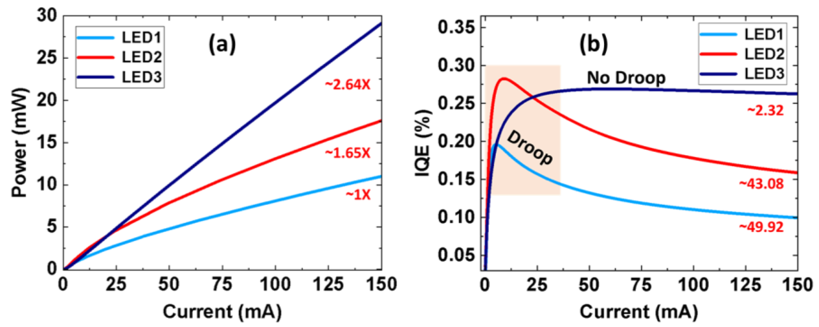
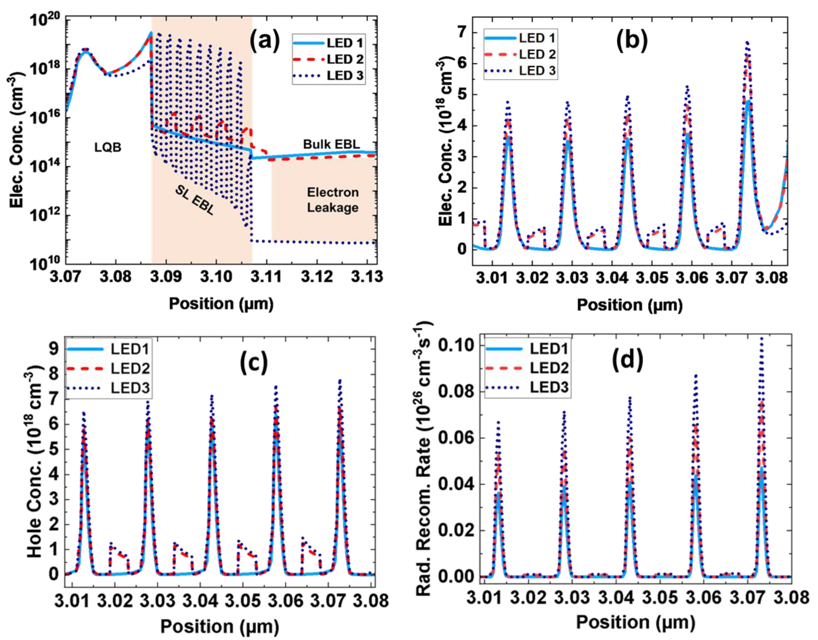
3. Results and Discussion

The calculated energy-band (E-B) diagrams of LED1, LED2, and LED3 at 150 mA current injection are shown in Figure 2a–c to understand their performance and carrier transport. The effective conduction band barrier height (CBBH), denoted as Φen, is defined as the maximum energy difference between the conduction band and its associated quasi-Fermi level for electrons within the QB(n). The estimated Φen values at the corresponding barrier (n) are provided in Table 1. It is seen that both LED2 and LED3 exhibited relatively lower Φen values compared to the conventional structure LED1. Previous studies [18,35] reported that the higher Φen values support the confining of electrons in the active region and prevent severe electron leakage into the p-region. Nevertheless, LED2 and LED3, with concave quantum barriers, show reduced electron leakage despite lower Φen values, due to decreased thermal velocity and a shorter electron mean free path in the active region [18,19].
Moreover, the Φe-EBL of the LED3 in the CBBH is the highest among all three designs because the SL EBL is crucial in minimizing electron leakage to p-region. Further, Φhn represents the effective valence band barrier height, measuring the maximum energy gap between the hole quasi-Fermi level and the valence band at each barrier (n). These values, derived from valence bands, are listed in Table 2. The Φhn values are lower in LED2 and LED3 than in LED1 because of the concave QBs, henceforth promoting better hole transportation into the AlGaN/AlGaN multi-QW region. Additionally, the Φh-EBL in LED3, associated with the valence band barrier height (VBBH), is lower than that in LED1 and LED2, facilitating improved hole transport from the p-region to the quantum wells (QWs). The electroluminescence (EL) spectra of all three LEDs are depicted in Figure 2d. The EL intensity of LED3 is higher than that of LED1 and LED2 at the emission wavelength of ~253.7 nm due to the improved radiative recombination.
The transport and capture behavior of electrons in the active region were systematically analyzed by calculating their thermal velocities and mean free paths (MFPs) across different LED configurations. The thermal velocity (vth) was derived from the sum of electron kinetic energy and work done by the internal electric field, while the electron MFP (lMFP) was computed as a product of (vth) and the electron scattering time (τsc) as shown in an Equation (3).
l M F P = v t h × τ s c
LED1, which uses conventional quantum barriers (QBs), exhibits the highest electron thermal velocity, denoted as vth(1), due to fewer scattering events and minimal structural complexity. In contrast, LED2 and LED3 implement concave-shaped QBs, which introduce additional scattering mechanisms that lower the carrier velocities, denoted as vth(2,3−a) and vth(2,3−b), respectively, as shown in Equations (4)–(7).
v t h 1 = 2 × E 1 + W 1 m e
v t h 2,3 a = 2 × E 2,3 a + W 2,3 a m e
v t h ( 2,3 b ) = 2 × E 2,3 a + Δ E + W 2,3 a ћ ω Δ E m e
v t h 2,3 b = 2 × E 2,3 a + W 2,3 a ћ ω m e
W y = q 0 t Q B   E y d y
where E(1) = 87.2 meV and E(2,3−a) = 87.7 meV are additional kinetic energies (K.E.) in the previous layer of QB2 with respect to its conduction band of LED1 and LED3. The W(1) = 84.5 meV and W(2,3−a) = 67.6 meV are work done to the electrons by the generated local electric field in QB2 of LED1 and LED3, respectively. The probability of electron capture in the QW is governed by a first-order exponential function of QW thickness (tQB) and MFP, as described in Equation (8).
As illustrated in Figure 3, six electron transport processes are defined to describe the mechanisms occurring in the QW region. A portion of the injected electrons (Ninit) enters the QB region and is scattered and captured in the quantum well (QW), forming a subset Ncinit as described in Equation (9) [36]. These carriers are available for radiative recombination and constitute the desired optical emission pathway, as shown in Process (1). A fraction of Ncinit undergoes radiative recombination with holes in the QW, contributing to light emission. Some may also recombine non-radiatively via defect centers, reducing internal quantum efficiency (IQE) in Process (2). Process (3) shows the electrons that initially enter the QW but acquire sufficient kinetic energy due to high field gradients escape the well before recombining. This escape results in an undesired leakage into the p-region. Some electrons possess a mean free path (MFP) longer than the QW thickness and bypass the QW entirely, never becoming confined, as shown in Process (4). These free carriers contribute directly to electron overflow and energy loss.
N c i n i t = N i n i t × 1 exp t Q W l M F P i n i t
where tQW is the quantum well (QW) thickness and lMFPinit is the electron mean free path in LED1. In LED3, two additional processes are introduced due to the use of concave QBs. A subset of Ninit, denoted as N(1), experiences LO phonon scattering in the Al0.67Ga0.33N barrier layer before reaching the QW. This phonon-carrier interaction redistributes the electrons’ kinetic energy and significantly reduces their thermal velocity (vth(2,3−a)) through momentum scattering Equation (3). The cooling effect enhances electron capture by decreasing the MFP, as shown in Process (5) [37]. The +ΔE in Equation (6) represents the K.E. received by the electrons when crossing the band offset between the n-Al0.7Ga0.3N and n-Al0.67Ga0.33N layers. The −ΔE is the energy lost by electrons while jumping from the n-Al0.67Ga0.33N layer during Process (5) in LED3. Also, ћω = 106.75 meV [38] is the energy lost due to LO phonon emission during the scattering in process (5) of LED3. Here, the effective mass of the electrons is considered as me. Therefore, the calculated thermal velocity values of vth(1), vth(2,3−a), and vth(2,3−b) are 2.46 × 10⁷ cms−1, 2.34 × 10⁷ cms−1, and 1.31 × 10⁷ cms−1 respectively. The remaining carriers, N(2) = Ninit − N(1), cross the barrier without significant scattering, as from Process (6). These electrons, having retained higher thermal energies, are less likely to be captured but still interact with the QW with some probability. The total number of captured electrons in LED3, accounting for both N(1) and N(2), is calculated using the two-path probability expression in Equation (10).
N c 1 = N 1 × 1 exp t Q W l M F P 1 + N 2 × 1 exp t Q W l M F P 2
Subsequently, the electron MFP at τsc = 0.0045 ps [39] for above all cases would be 1.11 nm, 1.05 nm, and 0.59 nm, respectively. Across all structures, the electron thermal velocities and MFPs follow the trend: vth(1) > vth(2,3−a) > vth(2,3−b) and lMFP(1) > lMFP(2,3−a) > lMFP(2,3−b). These reductions in thermal velocity and MFP in LED2 and LED3 promote stronger confinement of carriers in the QW, thereby suppressing leakage into the p-region and enhancing the radiative recombination rate. Additionally, the electrostatic fields at the last quantum barrier (LQB)/electron blocking layer (EBL) interface can further affect carrier confinement. A high polarization-induced field can lower the conduction band edge and degrade carrier confinement. This can be mitigated by reducing the EBL thickness or modifying the net polarization-induced charge density as described in Equations (11) and (12) [40].
E b I E B L . Δ P I E B L . ε b + I b . ε E B L
Δ P z = σ s P o l z = 0 ρ B P o l z z < l b
where Eb is the electrostatic field in the barrier, Ib and IEBL are the thicknesses of the barrier and EBL, respectively, and εb and εEBL represent the dielectric constants of the barrier and EBL. The σsPol is polarization-induced sheet charge density, and ρBPol is polarization-induced bulk charge density. ΔP represents the net polarization charge density. In LED3, a superlattice EBL composed of thin alternating AlGaN layers (2 nm in the first period) is employed, compared to 4.5 nm in LED2 and 20 nm in LED1. This finely tuned structure minimizes the internal field at the LQB/EBL junction, improving carrier confinement and enhancing wavefunction overlap, which leads to better internal quantum efficiency. Overall, the optimized concave QB and superlattice EBL design in LED3 effectively supports strong electron-hole recombination, lowers thermal velocity and leakage, and achieves superior device performance compared to conventional structures.
To elucidate the enhancement in carrier transport observed in the proposed concave quantum barriers (QBs) with superlattice electron blocking layer (SL-EBL) structure, designated as LED3, we conducted comprehensive simulations of light output-current (L-I) characteristics and internal quantum efficiency (IQE) for all three LED configurations. The results are presented in Figure 4. Analysis of the output power as a function of injection current reveals that LED3 demonstrates a significant improvement, exhibiting approximately 2.64 times higher output power compared to LED1 at an injection current of 150 mA, as illustrated in Figure 4a. A comparative summary of efficiency and output parameters for all LED configurations is provided in Table 3. Figure 4b depicts the IQE characteristics, where LED3 exhibits superior performance with a maximum IQE of 26.2% at 150 mA current injection. In contrast, LED1 and LED2 achieve IQE values of only 9.8% and 16.5%, respectively, under identical injection conditions. Furthermore, LED3 demonstrates remarkable stability in efficiency, with a minimal IQE droop of approximately 2.32% over the 0–150 mA injection current range. This represents a substantial improvement compared to the pronounced efficiency droop observed in LED1 (49.92%) and LED2 (43.08%) over the same current range. This is attributed to the improved radiative recombination and reduced carrier leakage, owing to the superior carrier confinement provided by the structure of LED3.
Table 4 summarizes the performance comparison of various AlGaN-based Deep UV LED structures reported in the literature alongside our proposed design, specifically focusing on the presence of a strip-in-a-barrier (concave quantum barrier) structure. Conventional designs, such as staggered and polarization-matched quantum wells, show moderate internal quantum efficiency (IQE) and output power but suffer from higher efficiency droop due to poor carrier confinement. Superlattice electron blocking layer (SL-EBL) designs improve hole injection and leakage suppression but lack electron transport control. Designs incorporating only concave QBs (strip-in-a-barrier) enhance electron confinement, improving IQE and output power. Notably, our proposed structure achieves a significantly higher output power (29 mW) and IQE (26.2%) with minimal efficiency droop (~2.3%) at 150 mA injection current, demonstrating the advantage of simultaneous electron and hole transport engineering through a hybrid barrier approach.
The electron concentration, hole concentration, and radiative recombination rate for the three LED structures were quantitatively analyzed at an injection current of 150 mA. Figure 5a illustrates the electron concentration profile beyond the active region, demonstrating that LED3 exhibits reduced electron leakage into the p-region compared to LED1. Notably, the proposed structure (LED3) achieves a significant reduction in electron leakage, ~4 orders of magnitude lower than the conventional structure (LED1). This enhanced electron confinement in LED3 can be attributed to the collective effect of reduced electron thermal velocity and MFP within the active region, coupled with an increased effective conduction band barrier height at the electron blocking layer (EBL) [21,22]. This mechanism mitigates the nonradiative recombination of leaked electrons with holes in the p-side, thereby increasing the availability of holes for injection into the active region. Furthermore, LED3 exhibits a lower effective valence band barrier height (VBBH) (Φhn) for hole injection compared to LED1 and LED2. This optimization leads to enhanced electron and hole concentrations in the active region of LED3, surpassing those of LED1 and LED2, as depicted in Figure 5(b),(c), respectively. Subsequently, radiative recombination is improved significantly due to the higher carrier concentration in the multi-QWs of LED3 compared to LED1 and LED2 as shown in Figure 5d. For real-time applications where high-current operation is required, such as UV curing, water sterilization, and high-density displays, an LED with a low droop percentage ensures consistent efficiency even while operating at high power.

4. Conclusions

This study presents unique lens-shaped QBs with a thin superlattice EBL LED construction that operates at ~253.7 nm wavelength. The proposed LED structure could notably slow down the hot electrons, thereby reducing the electron thermal velocity and mean free path, greatly improving the carrier confinement in the QWs and significantly reducing the electron overflow from the active region. In addition, SL-EBL helps with hole transportation and reduces droop efficiency. As a result, the proposed LED structure has reduced electron leakage by four orders of magnitude, improved electron and hole injection into the active region, increased efficiency by 2.67 times with the lowest droop of 2.32%, and increased output power by 2.64 times compared to conventional EBL LED. This arrangement is a viable method for developing high-efficiency UV light emitters for practical applications.

Author Contributions

Conceptualization, M.B.S.M., R.T.V., B.J. and H.P.T.N.; Methodology, M.B.S.M., R.T.V. and B.J.; Software, M.B.S.M.; Validation, R.T.V. and H.P.T.N.; Formal analysis, M.B.S.M., R.T.V., B.J. and H.P.T.N.; Investigation, M.B.S.M., R.T.V., B.J. and H.P.T.N.; Resources, B.J.; Writing—original draft, M.B.S.M. and R.T.V.; Writing—review & editing, M.B.S.M., R.T.V. and H.P.T.N.; Supervision, H.P.T.N. All authors have read and agreed to the published version of the manuscript.

Funding

The National Science Foundation under Grant No. ECCS- 2419509 supported this work.

Data Availability Statement

The data and materials are available upon request.

Acknowledgments

The authors would like to thank Texas Tech University and acknowledge financial support from the US National Science Foundation.

Conflicts of Interest

The authors declare no conflicts of interest.

Abbreviations

The following abbreviations are used in this manuscript:
CBBHConduction Band Barrier Height
EBLElectron Blocking Layer
IQEInternal Quantum Efficiency
LEDsLight Emitting Diodes
MFPMean Free Path
MQWsMultiple Quantum Wells
QBsQuantum Barriers
SLSuperlattice
UVUltraviolet
VBBHValence Band Barrier Height

References

  1. Feng, F.; Liu, Y.; Zhang, K.; Yang, H.; Hyun, B.R.; Xu, K.; Kwok, H.S.; Liu, Z. High-power AlGaN deep-ultraviolet micro-light-emitting diode displays for mask less photolithography. Nat. Photonics 2024, 19, 101–108. [Google Scholar] [CrossRef]
  2. Liu, X.; Lv, Z.; Liao, Z.; Sun, Y.; Zhang, Z.; Sun, K.; Zhou, Q.; Tang, B.; Geng, H.; Qi, S.; et al. Highly efficient AlGaN-based deep-ultraviolet light-emitting diodes: From bandgap engineering to device craft. Microsyst. Nanoeng. 2024, 10, 110. [Google Scholar] [CrossRef]
  3. Xu, R.; Kang, Q.; Zhang, Y.; Zhang, X.; Zhang, Z. Research progress of AlGaN-based deep ultraviolet light-emitting diodes. Micromachines 2023, 14, 844. [Google Scholar] [CrossRef]
  4. Li, D.; Jiang, K.; Sun, X.; Guo, C. AlGaN photonics: Recent advances in materials and ultraviolet devices. Adv. Opt. Photon. 2018, 10, 43–110. [Google Scholar] [CrossRef]
  5. Khan, M.A.; Maeda, N.; Itokazu, Y.; Jo, M.; Iimura, K.; Hirayama, H. Milliwatt-Power AlGaN Deep-UV Light-Emitting Diodes at 254 nm Emission as a Clean Alternative to Mercury Deep-UV Lamps. Phys. Status Solidi A 2023, 220, 2200621. [Google Scholar] [CrossRef]
  6. Muramoto, Y.; Kimura, M.; Nouda, S. Development and future of ultraviolet light-emitting diodes: UV-LED will replace the UV lamp. Semicond. Sci. Technol. 2014, 29, 084004. [Google Scholar] [CrossRef]
  7. Malik, S.; Usman, M.; Khan, M.A.; Hirayama, H. Polarization-dependent hole generation in 222 nm-band AlGaN-based Far-UVC LED: A way forward to the epi-growers of MBE and MOCVD. J. Mater. Chem. C 2021, 9, 16545–16557. [Google Scholar] [CrossRef]
  8. Song, K.; Mohseni, M.; Taghipour, F. Application of ultraviolet light-emitting diodes (UV-LEDs) for water disinfection: A review. Water Res. 2016, 94, 341–349. [Google Scholar] [CrossRef]
  9. Yeh, N.G.; Wu, C.-H.; Cheng, T.C. Light-emitting diodes—Their potential in biomedical applications. Renew. Sust. Energ. Rev. 2010, 14, 2161–2166. [Google Scholar] [CrossRef]
  10. Heilingloh, C.S.; Aufderhorst, U.W.; Schipper, L.; Dittmer, U.; Witzke, O.; Yang, D.; Zheng, X.; Sutter, K.; Trilling, M.; Alt, M.; et al. Susceptibility of SARS-CoV-2 to UV irradiation. Am. J. Infect. Control 2020, 48, 1273–1275. [Google Scholar] [CrossRef]
  11. Fan, S.-W.; Srivastava, A.K.; Dravid, V.P. UV-activated room temperature gas sensing mechanism of polycrystalline ZnO. Appl. Phys. Lett. 2009, 95, 142106. [Google Scholar] [CrossRef]
  12. Zhang, J.; Hu, X.; Lunev, A.; Deng, J.; Bilenko, Y.; Katona, T.M.; Shur, M.S.; Gaska, R.; Khan, M.A. AlGaN deep-ultraviolet light-emitting diodes. Jpn. J. Appl. Phys. 2005, 44, 7250. [Google Scholar] [CrossRef]
  13. Kneissl, M.; Seong, T.-Y.; Han, J.; Amano, H. The emergence and prospects of deep-ultraviolet light-emitting diode technologies. Nat. Photonics 2019, 13, 233–244. [Google Scholar] [CrossRef]
  14. Simon, J.; Protasenko, V.; Lian, C.; Xing, H.; Jena, D. Polarization induced hole doping in wide–band-gap uniaxial semiconductor heterostructures. Science 2010, 327, 60–64. [Google Scholar] [CrossRef]
  15. Nguyen, H.P.T.; Cui, K.; Zhang, S.; Djavid, M.; Korinek, A.; Botton, G.A.; Mi, Z. Controlling electron overflow in phosphor-free InGaN/GaN nanowire white light-emitting diodes. Nano Lett. 2012, 12, 1317–1323. [Google Scholar] [CrossRef]
  16. Ding, K.; Avrutin, V.; Özgür, Ü.; Morkoç, H. Status of growth of group III-nitride heterostructures for deep ultraviolet light-emitting diodes. Crystals 2017, 7, 300. [Google Scholar] [CrossRef]
  17. Zhang, M.; Li, Y.; Chen, S.; Tian, W.; Xu, J.; Li, X.; Wu, Z.; Fang, Y.; Dai, J.; Chen, C. Performance improvement of AlGaN-based deep ultraviolet light-emitting diodes by using staggered quantum wells. Superlattices Microstruct. 2014, 75, 63–71. [Google Scholar] [CrossRef]
  18. Velpula, R.T.; Jain, B.; Bui, H.Q.T.; Shakiba, F.M.; Jude, J.; Tumuna, M.; Nguyen, H.D.; Lenka, T.R.; Nguyen, H.P.T. Improving carrier transport in AlGaN deep-ultraviolet light-emitting diodes using a strip-in-a-barrier structure. Appl. Opt. 2020, 59, 5276–5281. [Google Scholar] [CrossRef]
  19. Jain, B.; Muthu, M.B.S.; Velpula, R.T.; Nguyen, N.T.A.; Nguyen, H.P.T. Advantages of concave quantum barriers in AlGaN deep ultraviolet light-emitting diodes. In Proceedings of the Gallium Nitride Materials and Devices XVIII 2023, San Francisco, CA, USA, 30 January–2 February 2023; SPIE: Bellingham, WA, USA, 2023; Volume 12421, pp. 143–148. [Google Scholar] [CrossRef]
  20. Jain, B.; Velpula, R.T.; Bui, H.Q.T.; Tumuna, M.; Jude, J.; Nguyen, H.P.T. Electron blocking layer free AlGaN deep-ultraviolet light emitting diodes. In Proceedings of the 2020 Conference on Lasers and Electro-Optics (CLEO), San Jose, CA, USA, 10–15 May 2020. AF1I-3. [Google Scholar] [CrossRef]
  21. Nguyen, H.P.T.; Djavid, M.; Woo, S.Y.; Liu, X.; Connie, A.T.; Sadaf, S.; Wang, Q.; Botton, G.A.; Shih, I.; Mi, Z. Engineering the carrier dynamics of InGaN nanowire white light-emitting diodes by distributed p-AlGaN electron blocking layers. Sci. Rep. 2015, 5, 7744. [Google Scholar] [CrossRef]
  22. Jain, B.; Velpula, R.T.; Velpula, S.; Nguyen, H.D.; Nguyen, H.P.T. Enhanced hole transport in AlGaN deep ultraviolet light-emitting diodes using a double-sided step graded superlattice electron blocking layer. J. Opt. Soc. Am. B 2020, 37, 2564–2569. [Google Scholar] [CrossRef]
  23. Li, Y.; Chen, S.; Tian, W.; Wu, Z.; Fang, Y.; Dai, J.; Chen, C. Advantages of AlGaN-based 310-nm UV light-emitting diodes with Al content graded AlGaN electron blocking layers. IEEE Photonics J. 2013, 5, 8200309. [Google Scholar] [CrossRef]
  24. Schubert, E.; Grieshaber, W.; Goepfert, I. Enhancement of deep acceptor activation in semiconductors by superlattice doping. Appl. Phys. Lett. 1996, 69, 3737–3739. [Google Scholar] [CrossRef]
  25. Kozodoy, P.; Hansen, M.; DenBaars, S.P.; Mishra, U.K. Enhanced Mg doping efficiency in Al0.2 Ga0.8N/ GaN superlattices. Appl. Phys. Lett. 1999, 74, 3681–3683. [Google Scholar] [CrossRef]
  26. Saxler, A.; Mitchel, W.; Kung, P.; Razeghi, M. Aluminum gallium nitride short-period superlattices doped with magnesium. Appl. Phys. Lett. 1999, 74, 2023–2025. [Google Scholar] [CrossRef]
  27. Goepfert, I.; Schubert, E.; Osinsky, A.; Norris, P. Demonstration of efficient p-type doping in AlxGa1–xN/ GaN superlattice structures. Electron. Lett. 1999, 35, 1109–1111. [Google Scholar] [CrossRef]
  28. Yan, J.; Wang, J.; Zhang, Y.; Cong, P.; Sun, L.; Tian, Y.; Zhao, C.; Li, J. AlGaN-based deep-ultraviolet light-emitting diodes grown on high quality AlN template using MOVPE. J. Cryst. Growth 2015, 414, 254–257. [Google Scholar] [CrossRef]
  29. Fiorentini, V.; Bernardini, F.; Ambacher, O. Evidence for nonlinear macroscopic polarization in III–V nitride alloy heterostructures. Appl. Phys. Lett. 2002, 80, 1204–1206. [Google Scholar] [CrossRef]
  30. Piprek, J. (Ed.) Nitride Semiconductor Devices: Principles and Simulation; Wiley: Hoboken, NJ, USA, 2007. [Google Scholar] [CrossRef]
  31. Nam, K.B.; Nakarmi, M.L.; Li, J.; Lin, J.Y.; Jiang, H.X. Mg acceptor level in AlN probed by deep ultraviolet photoluminescence. Appl. Phys. Lett. 2003, 83, 878–880. [Google Scholar] [CrossRef]
  32. Yun, J.; Shim, J.I.; Hirayama, H. Analysis of efficiency droop in 280-nm AlGaN multiple-quantum-well light-emitting diodes based on carrier rate equation. Appl. Phys. Express 2015, 8, 022104. [Google Scholar] [CrossRef]
  33. Collazo, R.; Mita, S.; Xie, J.; Rice, A.; Tweedie, J.; Dalmau, R.; Sitar, Z. Progress on n-type doping of AlGaN alloys on AlN single crystal substrates for UV optoelectronic applications. Phys. Status Solidi C 2011, 8, 2031–2033. [Google Scholar] [CrossRef]
  34. Coughlan, C.; Schulz, S.; Caro, M.A.; O’Reilly, E.P. Band gap bowing and optical polarization switching in Al Ga N alloys. Phys. Status Solidi B 2015, 252, 879–884. [Google Scholar] [CrossRef]
  35. Velpula, R.T.; Jain, B.; Velpula, S.; Nguyen, H.D.; Nguyen, H.P.T. High-performance electron-blocking-layer-free deep ultraviolet light-emitting diodes implementing a strip-in-a-barrier structure. Opt. Lett. 2020, 45, 5125–5128. [Google Scholar] [CrossRef]
  36. Zhang, Z.-H.; Liu, W.; Tan, S.T.; Ju, Z.; Ji, Y.; Kyaw, Z.; Zhang, X.; Hasanov, N.; Zhu, B.; Lu, S. On the mechanisms of InGaN electron cooler in InGaN/GaN light-emitting diodes. Opt. Express 2014, 22, A779–A789. [Google Scholar] [CrossRef]
  37. Zhang, X.; Taliercio, T.; Kolliakos, S.; Lefebvre, P. Influence of electron-phonon interaction on the optical properties of III nitride semiconductors. J. Phys. Condens. Matter 2001, 13, 7053–7074. [Google Scholar] [CrossRef]
  38. Kuball, M. Raman spectroscopy of GaN, AlGaN and AlN for process and growth monitoring/control. Surf. Interface Anal. 2001, 31, 987–999. [Google Scholar] [CrossRef]
  39. Mora-Ramos, M.; Gaggero-Sager, L. Electron-optical-phonon scattering rates in AlGaN/GaN-based single heterostructures. Phys. Status Solidi C 2005, 2, 3002–3005. [Google Scholar] [CrossRef]
  40. Zhang, Z.-H.; Liu, W.; Ju, Z.; Tan, S.T.; Ji, Y.; Kyaw, Z.; Zhang, X.; Wang, L.; Sun, X.W.; Demir, H.V. Self-screening of the quantum confined Stark effect by the polarization induced bulk charges in the quantum barriers. Appl. Phys. Lett. 2014, 104, 243501. [Google Scholar] [CrossRef]
Figure 1. Schematics of the LED structures: (a) The 3D design of AlGaN LED on Si substrate, (b) conduction band diagrams (at EBL) for LED1, LED2, and LED3 and (c) Al composition (%) profile related to the conduction band of conventional structure, i.e., LED1, concave EBL as LED2 and proposed SL EBL as LED3.
Photonics 12 00752 g001
Figure 2. Energy band diagrams of (a) LED1 (black), (b) LED2 (red), (c) LED3 (blue), and (d) Emission spectra of LED1, LED2, and LED3 at an injection current of 150 mA.
Photonics 12 00752 g002
Figure 3. Schematic of energy band diagram of the conventional LED1 and the proposed LED3.
Photonics 12 00752 g003
Figure 4. Calculated (a) power-current characteristics and (b) IQE-current characteristics of LED1, LED2, and LED3 at the injection current of 150 mA.
Photonics 12 00752 g004
Figure 5. Calculated (a) Electron leakage, (b) electron concentration, (c) hole concentration, and (d) radiative recombination rate in MQWs of LED1, LED2, and LED3 at an injection current of 150 mA.
Photonics 12 00752 g005
Table 1. Effective Conduction Band Barrier Heights (CBBH) of QBs (Φen) for LED1, LED2, and LED3.
CBBHLED 1LED 2LED 3
Φe1173.7 meV160.6 meV154.8 meV
Φe2177.6 meV160.8 meV156.1 meV
Φe3177.8 meV160.0 meV154.8 meV
Φe4176.7 meV158.5 meV153.2 meV
Φe5173.3 meV155.6 meV149.7 meV
Φe644.3 meV43.9 meV38.7 meV
Φe-EBL226.7 meV233.1 meV244.3 meV
Table 2. Effective Valence Band Barrier Heights (VBBH) of QBs (Φhn) for LED1, LED2, and LED3.
VBBHLED 1LED 2LED 3
Φh2278.7 meV266.4 meV261.2 meV
Φh3278.8 meV268.7 meV261.5 meV
Φh4280.3 meV268.9 meV263.4 meV
Φh5281.4 meV269.3 meV265.1 meV
Φh-EBL389.5 meV380.2 meV341.9 meV
Table 3. Comparison of efficiency (IQE) and the output power of LED1, LED2, and LED3.
LED
Structures
Max. IQE
(%)
IQE at
150 mA (%)
IQE Droop
at 150 mA (%)
Power at
150 mA (mW)
LED119.89.849.9211.01
LED228.616.543.0818.12
LED326.826.22.3229.04
Table 4. Comparison of IQE, power, and efficiency droop among various deep-UV LED designs.
S.NoLED DesignIQE (%)Output Power
(mW)
Efficiency Droop (%)
1Staggered QWs [17]~25~15~20
2Double-sided step graded SL EBL [22]24.215.689.1
3A strip-in-a-barrier structure [18,35]53.8721.2312.4
4Concave QBs (no SL-EBL) [19]3110.347.6
5Proposed LED Design
(Concave QBs + SL-EBL)
26.2 12.9
(at 60 mA)
<1
(at 60 mA)
Disclaimer/Publisher’s Note: The statements, opinions and data contained in all publications are solely those of the individual author(s) and contributor(s) and not of MDPI and/or the editor(s). MDPI and/or the editor(s) disclaim responsibility for any injury to people or property resulting from any ideas, methods, instructions or products referred to in the content.

