Article

On-Chip Mid-Infrared Dual-Band Wavelength Splitting with Integrated Metalens and Enhanced Bandwidth

1
College of Electrical and Information Engineering, Quzhou University, Quzhou 324000, China
2
Guangdong Provincial Key Laboratory of Optical Fiber Sensing and Communications, College of Physics and Optoelectronic Engineering, Jinan University, Guangzhou 511443, China
*
Author to whom correspondence should be addressed.
Photonics 2025, 12(7), 736; https://doi.org/10.3390/photonics12070736
Submission received: 16 June 2025 / Revised: 5 July 2025 / Accepted: 18 July 2025 / Published: 19 July 2025
(This article belongs to the Special Issue Infrared Optoelectronic Materials and Devices)

Abstract

On-chip spectral splitting structures with compact footprints hold tremendous potential for next-generation molecular sensing applications in the mid-infrared region. Here, we propose and theoretically investigate a carefully designed structure comprising a tilt grating and metalenses for dual-band spectral splitting with enhanced bandwidth. The tilt grating serves to separate the wavelength bands, and the metalenses following the grating guarantee a smooth transition of light into single-mode waveguides, giving rise to transmittances of 73.59% at 4 μm and 68.74% at 11 μm. The use of this tandem structure results in a significant footprint reduction and a remarkable 25.8% bandwidth enhancement over conventional approaches. The proposed spectral splitting scheme, with its broad wavelength range applicability, unlocks new pathways for on-chip simultaneous multi-target molecule detection.

1. Introduction

The mid-infrared region (2–14 μm) is an important part of the electromagnetic spectrum, as it comprises the characteristic absorption peaks of many molecules. This makes mid-infrared (mid-IR) spectroscopy a powerful tool for chemical substance analysis [1,2,3]. In environmental monitoring, it can be used to detect pollutants in the atmosphere and harmful substances in water. In medical diagnosis, it helps with the early diagnosis and monitoring of diseases [4,5]. Compared to mid-IR bands, the near-IR band exhibits weaker and broader absorption features due to overtone vibrations, leading to lower molecular specificity and increased susceptibility to background interference from sunlight or ambient thermal radiation. Until now, the majority of the applications are limited to utilizing a single mid-IR band for analysis [6,7,8]. Dual-band mid-IR spectroscopy requires simultaneous acquisition of complementary spectral information from two different bands. This enriched dataset not only enhances the efficiency of chemical and material identification but also broadens the application scope of mid-IR sensing based on spectral absorption.
The maturity of silicon photonics has spurred the development of mid-IR integrated optoelectronic devices. In view of the merits of the mid-IR region, there is a natural motive to exploit it for on-chip spectroscopy. However, a practical obstacle one has to face is the lack of an efficient mid-IR light source that can be integrated directly onto optoelectronic chips [9,10]. As a popular solution, mid-IR lights can be introduced into in-plane optics through either grating coupling [11,12,13] or end-face coupling. Broadband sources are often used in spectroscopic measurements. For dual-band mid-IR spectroscopy, two wavelength bands of interest need to be picked out from the broad spectrum. In general, there are two approaches to achieving band splitting. The first one is to couple the broadband infrared (IR) light by a grating and accomplish the two-band splitting at the grating-waveguide interfaces. In 2022, we proposed a mid-infrared dual-band grating coupler based on the principle of cross-diffraction order matching, and high coupling efficiencies for two bands were achieved by simulation [14]. The second approach is to first end-face couple broadband IR light into a waveguide. However, due to mode-support constraints, dispersion, and other factors, a waveguide with a fixed width has trouble achieving both low-loss and long-distance transmission across a broad wavelength range. Therefore, an in-plane spectral splitting structure for mid-infrared waveguides should be introduced to perform wavelength splitting and separate transmission over a broad range via specially designed structures downstream of the waveguide.
In integrated photonics, two common structures are used for in-plane wavelength splitting: diffraction-based and wavelength resonance-based structures. The arrayed waveguide grating (AWG) and the etched diffraction grating (EDG) belong to the former group. The AWG structure was first proposed by Smit in 1988 [15]. Its working principle was based on multi-beam interference [16]. As a dense wavelength division multiplexing technology, the AWG was widely used in bandwidth expansion in communication networks due to its advantages, such as high wavelength resolution [17,18,19]. In 2020, Akca et al. achieved wavelength splitting with a working bandwidth of 190 nm and a channel spacing of 65 nm in the 1550 nm band through a cascaded AWG scheme. However, the overall size of the cascaded AWG device reached the centimeter scale, at 1.1 × 1.0 cm2 [20]. AWGs have recently been used in the mid-IR region. In 2023, Tushar et al. constructed a 5 × 1 AWG array structure. They achieved a spectral working range of 5.15–5.34 µm (i.e., 190 nm) with a device area of 1.87 mm2 [21]. Different from the AWG, the EDG does not rely on optical length changes to split the wavelength. Instead, it relies heavily on the grating interface diffraction for spectral splitting. Usually, it features a more compact structure compared to the AWG and hence can help reduce the consumed chip area. However, the downside is that EDGs pose much higher requirements for etching accuracy and smoothness than AWGs do [22]. In the mid-infrared (mid-IR) region, several studies reported the successful implementation of EDGs. Specifically, on the Ge-on-SOI platform, a spectral splitting with a wavelength range of ~150 nm centered around 5.2 μm was achieved. The fabricated device exhibited a footprint of 1.5 × 1.2 mm2, and the operating spectral range and device size still need further optimization [23].
As another group of components for spectral splitting, wavelength resonance-based structures, such as the micro-ring resonators (MRRs), offer certain advantages over the diffraction-based structures. They usually possess high wavelength selectivity and a significantly high Q factor [24,25,26,27]. Cascaded MRR structures have been employed for on-chip multi-wavelength splitting, but their spectral ranges are relatively narrow, restricting the spectral splitting bandwidth. In the near-infrared band, the cascaded micro ring resonators (MRRs) have accomplished a spectral working range of 93 nm, as reported in [28]. Subsequently, in 2022, researchers fabricated a spectral splitting device by utilizing a set of cascaded 4-channel microring resonators on the silicon nitride platform. This device achieved a working wavelength range of approximately 100 nm in the vicinity of 3.42 μm, as documented in [29]. Due to their structural complexity and high fabrication precision requirements, these structures may encounter issues such as limited integration density and crosstalk between different MRRs. Table 1 presents a performance comparison of wavelength splitting devices, including AWG, EDG, MRRs, and the device we proposed in this study, in terms of the wavelength, footprint, and bandwidth.
Despite these efforts, existing mid-IR spectral splitting structures still face several challenges, such as a large footprint, narrow spectral splitting bandwidth, and high processing accuracy requirements. It cannot meet the requirements of mid-infrared multi-component spectral absorption molecular sensing. In this paper, we propose an on-chip mid-IR spectral splitting structure with a small footprint. The efficacy of this structure was verified by finite difference time domain (FDTD) simulations. Without losing generality, two representative wavelength bands (centered, respectively, at 4 μm and 11 μm) were selected to showcase the operation principle of this spectral splitting structure. The optimized transmittance of the split 4-μm band was 73.59%. Notably, the spectral splitting FWHM bandwidth reached 607 nm, which exhibited a remarkable increase of 25.8%, as compared with the scenario lacking the in-plane metasurface lens structure. This study is expected to lay the foundation for the expansion of applications of mid-infrared on-chip spectral absorption molecular sensing.
This is of great significance for achieving high-sensitivity sensing of multi-molecule components in the broad wavelength range on the mid-infrared chip. Many molecules exhibit strong and specific absorption in the MIR region. For instance, certain volatile organic compounds (VOCs) may have signature peaks in the 4–5 μm range, while gases such as CH4 show distinct absorption in the 8–14 μm range. The composite structure proposed here addresses a major limitation of current schemes, that is, being confined to single-band detection, and unleashes more freedom for the design of mid-infrared on-chip molecular detectors. It also has potential application value in the fields of disease diagnosis based on breath analysis and biomedical development.

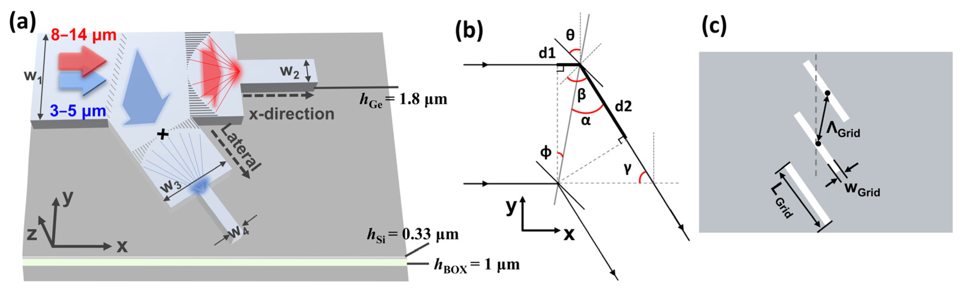
2. Design and Simulation of the Mid-IR Dual-Band Wavelength Splitting Device

The mid-IR dual-band wavelength splitting device proposed here is used to split the 3–5 μm wavelength band off the wide band (2–14 μm). Specifically, we introduced a tilt grating to alter the transmission direction of the 3–5 μm wavelength band without affecting the optical transmission path of other bands. Two center wavelengths (4 μm and 11 μm) from two wavelength bands (3–5 μm and 8–14 μm) were selected as the target wavelengths for optimization. The main effort of this work was directed to identifying the proper diffraction orders for the two wavelengths and broadening the bandwidth of the split-off 3–5 μm wavelength band through integrating the on-chip metasurface lens (metalens).
Figure 1a is a three-dimensional (3D) sketch of the proposed mid-IR dual-band wavelength splitting device constructed on a Ge-on-SOI platform, with a top Ge layer thickness of hGe = 1.8 μm, an upper silicon layer thickness of hSi = 0.33 μm, and a buried oxide thickness of hBOX = 1 μm. The broadband mid-IR (2–14 μm) light was assumed to transmit into the Ge waveguide through the left input port. The 3–5 μm wavelength band was split by the tilt grating and transmitted to the lateral direction. Then the on-chip metalenses focused the energies of two bands into the reduced-size waveguides with relatively low loss. At the same time the lateral metalens would broaden the spectral transmission bandwidth in the 3–5 μm wavelength band. As labeled in Figure 1a, w1 is the input waveguide width and w2 is the transmission waveguide width of the 8–14 μm wavelength band. w3 and w4 correspond to the width of the intermediate transmission waveguide and the width of the transmission waveguide of the 3–5 μm wavelength band, respectively. Figure 1b is a schematic diagram of the diffraction condition and the angle labeling of the tilt grating. A broadband light source is incident and transmitted in the x-direction and diffracts at the tilt grating. θ is the rotation angle of the grating grooves relative to the transverse direction, equal to the incident angle between the incident light and the normal. β is the angle between the diffracted light and the normal, which is the diffraction angle. The deflection angle γ is the angle between the diffracted light and the x-axis. φ is the overall tilt angle of the grating, and its change directly affects the optical path difference before diffraction, as shown by the thick solid line d1 in Figure 1b. The optical path difference after diffraction can be calculated by using the trigonometric function relationship of the angle α between the diffracted light and the grating tilt axis, as shown by the thick solid line d2 in this figure. Figure 1c shows the geometric parameters of the grating. Λ G r i d is the period of the grating, and it is defined as the distance between the center points of two adjacent grooves. W G r i d and L G r i d represent the width and length of the grating groove, respectively.
The relationships between the relevant angles and the optical path lengths can be derived from Figure 1b.
The optical path difference before the occurrence of diffraction is calculated as follows:
d 1 = Λ G r i d · sin φ
The optical path difference after hitting the grating can be calculated by the following equation:
d 2 = Λ G r i d · c o s α
In addition, α can be related to φ and γ with the following equation:
α = γ φ
The diffraction grating condition, the difference in optical path and the incident wavelength λ need to be fulfilled:
m λ = n · d 1 + d 2
The design rationale for band splitting utilizing the tilted diffraction grating structure is presented below:
m λ = n · Λ G r i d sin φ + c o s γ φ
In this equation, m represents the diffraction order, and n denotes the effective refractive index value when the corresponding wavelength is transmitted in the Ge material.

3. Results and Discussion

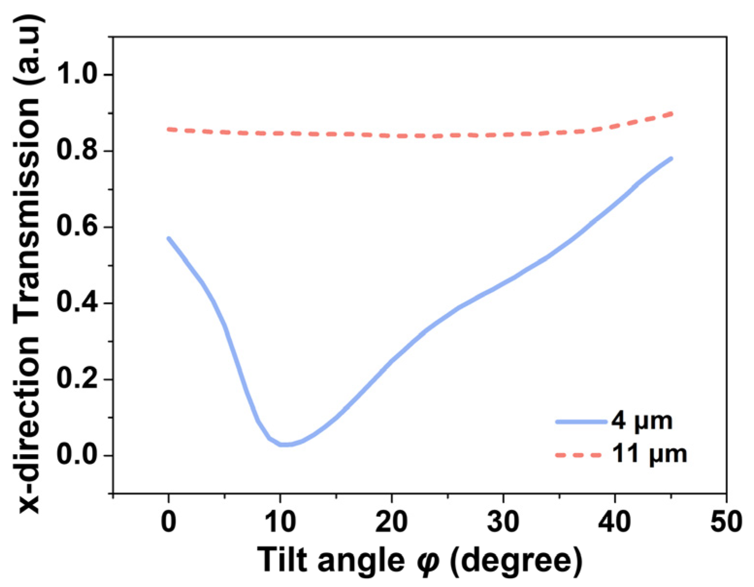
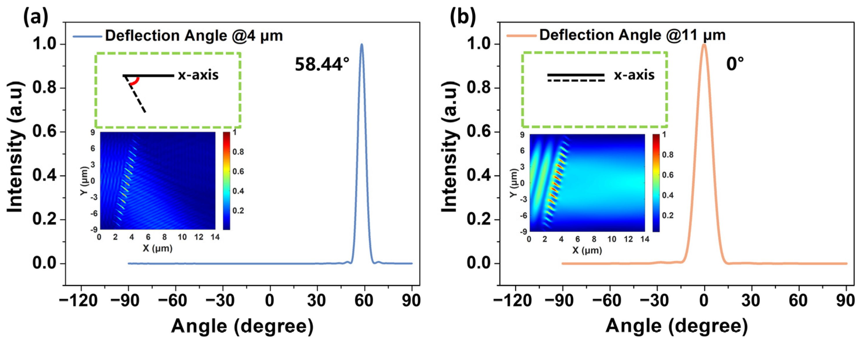
3.1. Tilt Grating for Mid-IR Dual-Band Splitting

The tilt grating is a key component of the proposed dual-band splitting device. The main function of the tilt grating is to screen out the 4 μm band from the incident broadband mid-IR light. The tilt grating is formed by a one-dimensional array of fully etched nano-grooves. In this work, the device is designed based on the Ge-on-SOI platform, and we mainly consider the transverse-electric polarization (TE) in the waveguide. In accordance with the grating diffraction theory, the diffraction orders of a diffraction grating are jointly determined by multiple factors, including the grating period, the length and width of the grating grooves, and the incident angle. Here, a tilt diffraction grating was employed to accomplish the spectral splitting of specific wavelengths. Subsequently, each of the grating parameters was subjected to iterative optimization procedures.
Firstly, the grating period was optimized while keeping other parameters fixed. As depicted in Figure 2a, for wavelengths of 4 μm and 11 μm, a parameter sweep was conducted over period values ranging from 0.5 μm to 3 μm. The evaluation metric was the transmittance monitored at the position after the grating structure. According to the simulation results, as the period increased, the x-direction transmittance at 11 μm gradually rose. When the period Λ G r i d exceeded 1 μm, the transmittance could exceed 80%. This indicates that light of 11 μm wavelength can essentially traverse the grating structure and keep propagating longitudinally without experiencing notable energy losses due to structural diffraction. Meanwhile, as the period increased, the transmittance of 4 μm wavelength light in the x-direction showed an oscillatory trend. When the period was 1.1 μm, the x-direction transmittance was nearly zero, and almost all the energy was concentrated in a certain diffraction order to propagate in directions other than the x-direction. That achieved beam deflection and splitting for the 4 μm wavelength band. We hereafter used a period of Λ G r i d = 1.1 μm for the rest of the optimization processes.
The optimization of the incident angle θ can affect the diffraction angle β and the diffraction order m. Based on the geometric relationship in Figure 1c, the incident angle is deduced to be equivalent to the grating tilt angle θ. Figure 2b shows the influence of the grating rotation angle on the transmittance in the x-direction. As the rotation angle of the grating changed from 0° (vertical grooves) to 90° (longitudinal grooves), the normalized transmittance showed a prominent minimum (3.11%) at 45° for the 4 μm band. The vast majority of the energy was transferred from zero-order to the first-order diffraction. For the 11 μm band, the normalized transmittance was 84.7% when θ was set to 45°. This indicates that at this angle the 11 μm wavelength light can essentially transmit the structure smoothly, and a small amount of energy was lost due to reflection and diffraction.
The length and width of the grating grooves also have a significant impact on the transmittance in the x-direction, as they determine the effective refractive index of the grating. Figure 2c,d display the color mappings of the 4-μm and 11-μm band transmittances as a function of the groove width and length. Here, we swept the length and the width in the range of 1–2 μm and 0.1–0.5 μm, respectively, and attempted to find an optimal x-direction transmittance for the 11-μm band while keeping the transmission of the 4-μm band at a minimum. To this end, we defined the following function of the figure of merit (FOM) to evaluate the optimization result:
F O M = 1 T λ 1 i , j + T λ 2 i , j
where T λ i , j represents the transmission of λ under the parameter combination of (i, j). i and j correspond to the two parameters to be optimized, and in this case, they are the groove width and length, respectively. Parameter ranges were defined as i 0.1 , 0.5   a n d   j [ 1 , 5 ] . The optimization objective is to obtain the lowest transmittance of the 4-μm band while having the highest possible transmittance of the 11-μm band in the x-direction. The two target wavelengths λ 1 and λ 2 for optimization were 4 μm and 11 μm, respectively. With Equation (6), an optimal transmittance combination of 84.09% (11 μm) and 2.8% (4 μm) was found while the groove length and width were set to 1.5 μm and 0.15 μm, respectively.
In addition to optimizing the rotation angle of the grating grooves, the overall tilt angle of the grating was also optimized. According to the principle of the diffraction grating, introducing the overall tilt angle φ of the grating enables the regulation of the incident optical path between the grooves. Consequently, parameter regulation based on the diffraction formula can be achieved. The x-direction transmittances of two bands as a function of the tilt angle φ are shown in Figure 3. As φ progressed from 0° to 45°, the transmittance curve of the 11-μm band remained essentially flat and maintained its values above 80%, indicating an insignificant effect of φ on the 11-μm band transmission. By contrast, the transmission curve for the 4-μm band showed an obvious dip (2.8%) at φ = 10°. This indicates that the majority of the 4-μm band energy was transferred to other diffraction orders at this tilt angle. Therefore, φ = 10° was chosen as the optimal tilt angle for our grating.
The tilt angle φ and the groove rotation angle θ together determine the deflection angles of the transmitted beams. These deflection angles can be extracted by looking at the data recorded at the far-field monitors. To do this, two monitors were set up after the spectral splitting grating, as indicated by dashed lines in Figure 1a. Specifically, one monitor with a width of 16 μm was placed above the lateral transmission waveguide, parallel to the x-axis; another with a width of 18 μm was placed perpendicular to the x-direction transmission waveguide along the y-axis. Figure 4a,b show the deflection angles of the 4-μm and 11-μm bands, respectively. The angles are defined as in the insets of the panels. After passing through the spectral splitting grating, the 4-μm band had a deflection angle of 58.44°, while the 11-μm band had a deflection angle of 0°.
Having obtained the deflection angles, we proceed to examine the electric field distribution of the two bands in detail. The upper parts of Figure 5a,b exhibit the cross-sections of the normalized electric field distribution for two bands at locations denoted by L and w1, respectively. The lower parts of these figures are cuts along the dashed line indicated in the upper parts. The electric field distribution of the 4-μm band (Figure 5a) basically resembles a quasi-Gaussian shape but is superimposed with oscillatory features. In essence, this oscillatory behavior originated from the diffraction effect. The diffraction due to the grating grooves formed multiple new wave sources. These waves arrived at L (~14.1 μm, marked in Figure 5c) and interfered with each other to form oscillatory patterns in the electric field distribution. The curve shown in the lower part of the figure allows us to observe more clearly the fluctuation of the electric field across the width L. From L and the deflection angle, a proper value for designing the width (w3) of the lateral transmission waveguide can be calculated, which was 12 μm. On the other hand, the effective field distribution width shown in Figure 5b was the same as that of the x-direction transmission waveguide, which was 18 μm. The overall electrical field distribution exhibits a quasi-Gaussian distribution.

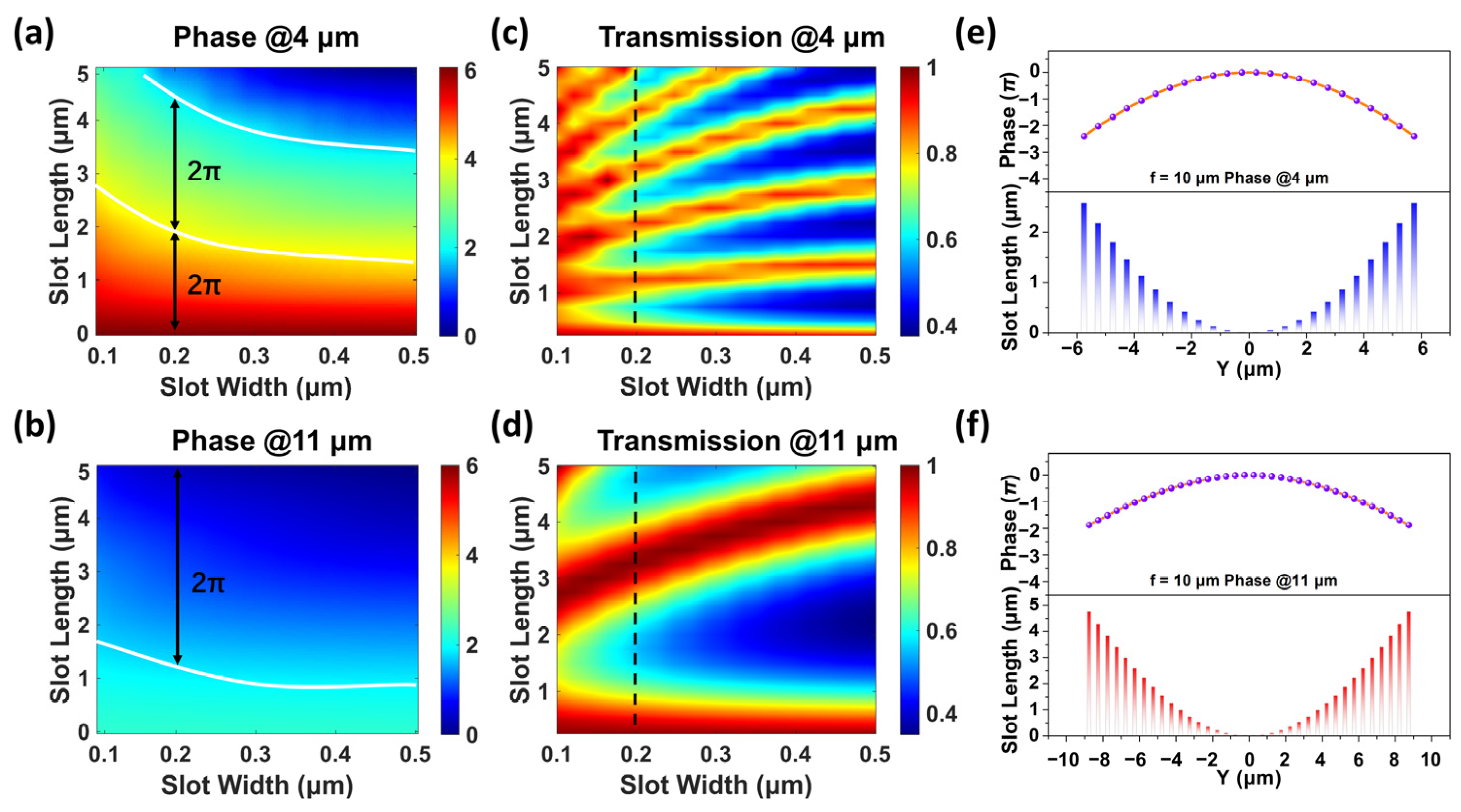
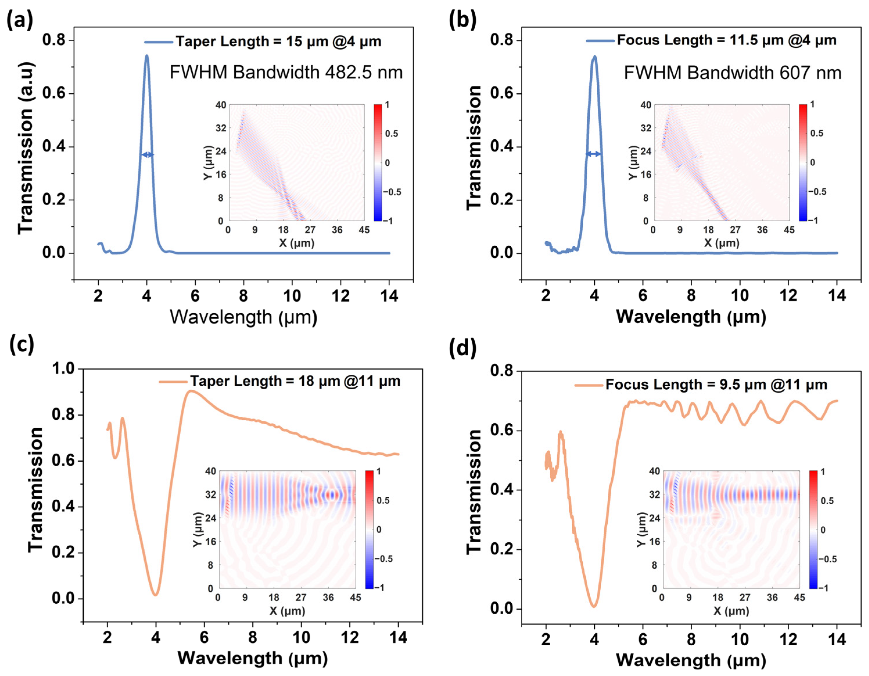
3.2. Light Coupling to Single-Mode Waveguide by Metalens

In Section 3.1, we have demonstrated a specially designed grating that can split certain wavelength bands off a broadband incident light. In this structure (Figure 5c), these bands, after splitting, propagated in relatively wide (>10 μm) waveguides. In practical applications, much narrower waveguides are preferred in order to reduce the effective footprint of the device and the propagation loss. In recent years, on-chip metalens technology has emerged as a revolutionary approach in photonics. In 2023, Luo et al. introduced a highly integrated on-chip metalens with remarkable coupling efficiency and integration, featuring an ultra-small longitudinal footprint of 2.35 μm and a numerical aperture of 2.03, enabling beam focusing and collimation within 10 μm [30]. In 2025, Wang et al. combined an on-chip metalens with topology optimization, achieving enhanced transmission efficiency in a compact mode converter; when integrated with a grating coupler, it achieved low insertion loss and significantly improved overall transmission efficiency [31]. These studies pave the way for footprint reduction, insertion loss minimization, high-sensitivity detection, and precise imaging in complex scenarios [32,33]. On the other hand, the application of metalenses in mid-IR wavelength splitting with large bandwidth still awaits further exploration. In the following, we attempt to use metalenses to facilitate a high-efficiency and large-bandwidth transition of the split-off bands into narrow waveguides.
The operation principle of propagation phase metalens relies on the phase control of the light through regulating the size of nanostructures [34]. In contrast to traditional optical systems, metalenses can achieve similar optical functions with a much more compact and lightweight form factor. The focusing metalens controls light waves through the phase modulation (0–2π) of micro-nano units. It replaces the continuous optical path accumulation method of each optical path in traditional lenses, thus enabling each light beam to converge at a preset position [35]. In on-chip focusing metalenses, the phase regulation is mainly achieved by adjusting the length and width of the air slots. Through rational design of the unit structure, a phase change of at least 2π must be achieved within a certain size range to meet the arbitrary phase modulation requirements [32,36,37]. For the metalens focusing the 11-μm band light, the structure imposes a location-dependent phase shift on the TE polarized light traveling along the x-direction. The phase change Φ(y) along the y direction can be described by the following equation [38,39]:
Φ y = 2 π λ n e f f y 2 + f 2 f
where λ is the wavelength of the incident light, neff is the effective refractive index, and f is the designed focal length. The optical path difference is given by Δ L = y 2 + f 2 f . By using this equation, the accumulated propagation phase of the electromagnetic wave can be obtained. During the design and construction of the 2π phase shift, phase change and transmission are the two crucial factors that need to be taken into account. To finely and continuously manipulate the phase of light at the sub-wavelength scale and effectively suppress the diffraction effect, and to enable light to propagate more intensively in the expected direction, we controlled the air slots’ period to be less than half of the target operating wavelength. For the design in this work, the period of the air slots was set to 500 nm. A nested scan was performed on the width and length of the air slots. The width was varied from 0.1 μm to 0.5 μm, and the length from 0 μm to 5 μm.
Figure 6a,b show the phase changes for the 4-μm and 11-μm bands, respectively, as the length and width of the air slots were swept. Both colorbars were set to a range of 0 to 6π. For the 4-μm band, it is evident from Figure 6a that at any width in the range, a phase change of 4π (or even more than 4π) can be achieved by varying the length. On the other hand, the 2π phase shift requirement could also be met for the 11-μm band by setting the width equal to or larger than 200 nm and choosing a proper length, as shown in Figure 6b. In addition to the phase shift, the impact of the slot dimension variation on the transmittance was also investigated, and the results are shown in Figure 6c,d. By picking a width, the transmittance exhibits a periodic change with the slot length. On the other hand, at a given slot length, a narrower width usually yields higher transmittance. However, a narrower slot width means that the phase shift in the 11-μm band might go below 2π, as can be seen in Figure 6b. To balance both outcomes of the phase shift and the transmittance, we chose to fix the slot width at 0.2 μm and manipulate the phase shift by varying the slot length.
According to Equation (6), we calculated the required phase change and the corresponding air slot structural dimensions for a designed focal length. In this study, we compared the transmission through the metalenses with three designed focal lengths: f = 5 μm, 10 μm, and 15 μm. Through comprehensive analysis, we found that the metalens structure with a focal length of 10 μm exhibited a favorable combination of transmittance and structural size economy. Figure 6e shows the phase shift for the 4-μm band as a function of slot length with a focal length of 10 μm. To fulfill the 2π requirement, the slot length was varied from 0 to 2.58 μm. Figure 6f shows the result for the 11-μm band. To achieve comparable phase shifts, larger slot lengths were required. The longest slot length reached 4.75 μm.
In order to achieve efficient focusing and low transmission loss, the finite difference eigenmode (FDE) simulation method was utilized here to evaluate the waveguide dimensions for ideal single-mode transmission for two central wavelengths. The output waveguide widths were set to w2 = 5 μm in the x-direction and w4 = 2 μm in the lateral direction. The distance between the focusing metalens’ starting position (as marked in Figure 1a) and the output waveguide was set equal to the focal length. Based on the previous discussion, a focal length of 10 μm was selected as a starting point for the design optimization. By evaluating the transmittances at various focus lengths (actual focal length) near 10 μm, we obtained optimal focus lengths of f1 = 11.5 μm and f2 = 9.5 μm for the 4-μm and 11-μm bands, respectively, and the corresponding transmittances were 73.59% and 68.74%.
Conventionally, tapered structures are often used to ensure a smooth and low-loss transition of light from wide to narrow waveguides. To further reveal the merits of the designed focusing metalens, we compare its performance to that of the tapered structures. Specifically, by assuming an identical peak transmittance at 4 μm, other performance parameters (i.e., bandwidth and footprint) of these two structures were scrutinized. Figure 7a,b present the comparison of the 4-μm band splitting and transmission with the tapered structure and the focusing metalens, respectively. It is clear that both structures can meet the spectral splitting and transmission requirements for the wavelength band centered at 4 μm. However, a closer look at the transmission curves revealed that the FWHM bandwidth of the metalens reached a value of 607 nm, which represented a significant improvement of 25.8% relative to that of the tapered structure.
Analyzing the electric field distributions shown in the insets of Figure 7a,b led us to postulate that the enhanced bandwidth was mainly due to the focusing effect of the metalens and relative insensitivity of the phase shift to the wavelength variation. Upon passing through the metalens, the wavelength band centered at 4 μm was focused towards the central axis, implying less interaction of these wavelengths with the side walls and the environment. As a result, the transmittance of the wavelengths adjacent to 4 μm generally fell off slower than that of the tapered structure did, contributing to an enhanced bandwidth. In addition, to achieve the same transmittance, the metalens measured 11.5 μm in the light propagation direction, which marked a reduction of 23.3% in length with respect to that (15 μm) of the tapered structure. Figure 7c,d exhibit the results of transmission in the x-direction for the nominal 11-μm band. It is apparent that the splitting grating essentially permitted a broadband transmission except for the 4-μm band. The utilization of the metalens at the downstream of the splitting grating yielded a more consistent transmission response in the 6–14 μm range than using a tapered structure. We remark that cascaded gratings can be used to split multiple bands (akin to the 4-μm band) off the broadband light and hence form multi-band outputs. A comparison of parameters related to the metalens focusing structure and the tapered structure is summarized in Table 2.
As the performance of both the metalens and grating structures is sensitive to geometric variations, we analyzed the fabrication tolerances of the proposed structure. Figure 8a,b illustrate the effect of variation in metalens slot width on the FWHM and transmission. When the metalens slot width increased from 0.05 μm to 0.125 μm, the FWHM decreased to a minimum of 545 nm and then increased monotonically with the slot width. Since a slot width of 0.2 μm was obtained in Figure 6, we focused on a variation range of 0.125 μm to 0.35 μm. Using a 10% performance degradation as the threshold, the tolerance range of the metalens slot width was determined to be 0.14–0.306 μm (≈166 nm). For the grating structure, we analyzed the effect of groove pitch (0.7–1.5 μm, Figure 8c) and groove width variations (0.05–0.25 μm, Figure 8d) on the transmission. Using transmission drops of 10% and 20% as criteria, we found that the tolerance range of the groove pitch for a 10% transmission drop was approximately ±30 nm and ±40 nm for a 20% drop. For the groove width, the tolerance ranges were approximately ±50 nm and ±70 nm for 10% and 20% drops, respectively.
For the practical fabrication of the proposed structure, established lithographic techniques offer robust solutions aligned with the identified dimensional tolerances. Electron beam lithography (EBL) stands out for its high resolution, enabling precise definition of subwavelength metalens features and nano-grooves within the required tolerance ranges. Additionally, given the minimum feature size of ~150 nm in the proposed structure, two-photon polymerization (TPP) emerges as a particularly compelling fabrication method [40,41]. It is capable of prototyping complex geometries with sub-100 nm precision. This makes TPP a promising technique to fabricate the structures proposed here.

4. Conclusions

In this work, we proposed and demonstrated by simulation a tilt-grating structure with integrated metalenses for high-efficiency splitting of the 3–5 μm band from a broadband source. Given a fixed transmittance, the length of the intermediate transmission devices, i.e., the metalenses, was significantly reduced. Specifically, for the 4-μm wavelength, the length of the on-chip focusing structure was shortened by 23.3% compared to the length of the tapered structure, and the entire footprint of the device was as small as 616.89 μm2. In addition, for the focusing transmission in the 3–5 μm band, the FWHM bandwidth of the on-chip focusing structure reached 607 nm, marking a significant increase of 25.8% compared to the tapered structure. The remarkable reduction in size not only renders the integration of the device into more compact optical systems more expeditious but also lays a solid foundation and clears the path for the development of miniaturized, portable devices based on spectral absorption sensing. Moreover, the scheme proposed here is expected to expand the versatility and detection efficiency of mid-IR on-chip spectroscopy. It may find immediate applications in simultaneous multi-target molecule detection by using integrated photonics. Eventually, we remark that while the current research is focused on simulation analysis and provides a theoretical framework for designing mid-IR wavelength-splitting devices, further experimental validation is essential to showcase the practical feasibility and performance of the proposed scheme.

Author Contributions

Conceptualization, D.H. and Y.Z.; methodology, D.H. and Q.Z.; software, D.H.; writing—original draft preparation, D.H.; writing—review and editing, Y.Z., Q.Z., Z.Y., and X.-M.D.; funding acquisition, Y.Z. and Z.Y. All authors have read and agreed to the published version of the manuscript.

Funding

This research was funded by the National Natural Science Foundation of China (62174071); the Major Talent Program of Guangdong Province (Grant No. 2021QN02X936); the Joint Fund of Zhejiang Provincial Natural Science Foundation of China (No. LQZSZ25F050001); Quzhou Science and Technology Plan Project (Nos. 2024K131 and 2024K158).

Institutional Review Board Statement

Not applicable.

Informed Consent Statement

Not applicable.

Data Availability Statement

Data are contained within the article.

Conflicts of Interest

The authors declare no conflicts of interest.

References

  1. Petersen, C.R.; Møller, U.; Kubat, I.; Zhou, B.; Dupont, S.; Ramsay, J.; Benson, T.; Sujecki, S.; Abdel-Moneim, N.; Tang, Z. Mid-infrared supercontinuum covering the 1.4–13.3 μm molecular fingerprint region using ultra-high NA chalcogenide step-index fibre. Nat. Photonics 2014, 8, 830–834. [Google Scholar] [CrossRef]
  2. Wang, L.; Mizaikoff, B. Application of multivariate data-analysis techniques to biomedical diagnostics based on mid-infrared spectroscopy. Anal. Bioanal. Chem. 2008, 391, 1641–1654. [Google Scholar] [CrossRef] [PubMed]
  3. Nikodem, M.; Krzempek, K.; Dudzik, G.; Abramski, K. Hollow core fiber-assisted absorption spectroscopy of methane at 3.4 µm. Opt. Express 2018, 26, 21843–21848. [Google Scholar] [CrossRef] [PubMed]
  4. Hinkov, B.; Pilat, F.; Lux, L.; Souza, P.L.; David, M.; Schwaighofer, A.; Ristanić, D.; Schwarz, B.; Detz, H.; Andrews, A.M. A mid-infrared lab-on-a-chip for dynamic reaction monitoring. Nat. Commun. 2022, 13, 4753. [Google Scholar] [CrossRef] [PubMed]
  5. Henderson, B.; Khodabakhsh, A.; Metsälä, M.; Ventrillard, I.; Schmidt, F.M.; Romanini, D.; Ritchie, G.A.; te Lintel Hekkert, S.; Briot, R.; Risby, T. Laser spectroscopy for breath analysis: Towards clinical implementation. Appl. Phys. B 2018, 124, 161. [Google Scholar] [CrossRef] [PubMed]
  6. Vlk, M.; Datta, A.; Alberti, S.; Yallew, H.D.; Mittal, V.; Murugan, G.S.; Jágerská, J. Extraordinary evanescent field confinement waveguide sensor for mid-infrared trace gas spectroscopy. Light Sci. Appl. 2021, 10, 26. [Google Scholar] [CrossRef] [PubMed]
  7. Zhu, J.; Ji, S.; Ren, Z.; Wu, W.; Zhang, Z.; Ni, Z.; Liu, L.; Zhang, Z.; Song, A.; Lee, C. Triboelectric-induced ion mobility for artificial intelligence-enhanced mid-infrared gas spectroscopy. Nat. Commun. 2023, 14, 2524. [Google Scholar] [CrossRef] [PubMed]
  8. Ren, Z.; Zhang, Z.; Wei, J.; Dong, B.; Lee, C. Wavelength-multiplexed hook nanoantennas for machine learning enabled mid-infrared spectroscopy. Nat. Commun. 2022, 13, 3859. [Google Scholar] [CrossRef] [PubMed]
  9. Lin, H.; Luo, Z.; Gu, T.; Kimerling, L.C.; Wada, K.; Agarwal, A.; Hu, J. Mid-infrared integrated photonics on silicon: A perspective. Nanophotonics 2017, 7, 393–420. [Google Scholar] [CrossRef]
  10. Hu, T.; Dong, B.; Luo, X.; Liow, T.-Y.; Song, J.; Lee, C.; Lo, G.-Q. Silicon photonic platforms for mid-infrared applications. Photonics Res. 2017, 5, 417–430. [Google Scholar] [CrossRef]
  11. Alonso-Ramos, C.; Nedeljkovic, M.; Benedikovic, D.; Penadés, J.S.; Littlejohns, C.G.; Khokhar, A.Z.; Pérez-Galacho, D.; Vivien, L.; Cheben, P.; Mashanovich, G.Z. Germanium-on-silicon mid-infrared grating couplers with low-reflectivity inverse taper excitation. Opt. Lett. 2016, 41, 4324–4327. [Google Scholar] [CrossRef] [PubMed]
  12. Radosavljevic, S.; Kuyken, B.; Roelkens, G. Efficient 5.2 µm wavelength fiber-to-chip grating couplers for the Ge-on-Si and Ge-on-SOI mid-infrared waveguide platform. Opt. Express 2017, 25, 19034–19042. [Google Scholar] [CrossRef] [PubMed]
  13. Hong, J.; Spring, A.M.; Qiu, F.; Yokoyama, S. A high efficiency silicon nitride waveguide grating coupler with a multilayer bottom reflector. Sci. Rep. 2019, 9, 12988. [Google Scholar] [CrossRef] [PubMed]
  14. Hu, D.; Zhang, Y.; Zhao, Y.-Y.; Duan, X.-M. Efficient 4.95 µm–8.5 µm dual-band grating coupler with crosstalk suppression capability. Opt. Express 2022, 30, 2131–2142. [Google Scholar] [CrossRef] [PubMed]
  15. Smit, M.K. New focusing and dispersive planar component based on an optical phased array. Electron. Lett. 1988, 24, 385–386. [Google Scholar] [CrossRef]
  16. Karnik, T.S.; Diehl, L.; Dao, K.P.; Du, Q.; Pflügl, C.; Vakhshoori, D.; Hu, J. Monolithic beam combined quantum cascade laser arrays with integrated arrayed waveguide gratings. Opt. Express 2024, 32, 11681–11692. [Google Scholar] [CrossRef] [PubMed]
  17. Stanton, E.; Spott, A.; Davenport, M.; Volet, N.; Bowers, J. Low-loss arrayed waveguide grating at 760 nm. Opt. Lett. 2016, 41, 1785–1788. [Google Scholar] [CrossRef] [PubMed]
  18. Fotiadis, K.; Pitris, S.; Moralis-Pegios, M.; Mitsolidou, C.; De Heyn, P.; Van Campenhout, J.; Broeke, R.; Alexoudi, T.; Pleros, N. Silicon photonic 16× 16 Cyclic AWGR for DWDM O-band interconnects. IEEE Photonics Technol. Lett. 2020, 32, 1233–1236. [Google Scholar] [CrossRef]
  19. Gatkine, P.; Veilleux, S.; Hu, Y.; Bland-Hawthorn, J.; Dagenais, M. Arrayed waveguide grating spectrometers for astronomical applications: New results. Opt. Express 2017, 25, 17918–17935. [Google Scholar] [CrossRef] [PubMed]
  20. van Wijk, A.; Doerr, C.R.; Ali, Z.; Karabiyik, M.; Akca, B.I. Compact ultrabroad-bandwidth cascaded arrayed waveguide gratings. Opt. Express 2020, 28, 14618–14626. [Google Scholar] [CrossRef] [PubMed]
  21. Karnik, T.S.; Dao, K.P.; Du, Q.; Diehl, L.; Pflügl, C.; Vakhshoori, D.; Hu, J. High-efficiency mid-infrared InGaAs/InP arrayed waveguide gratings. Opt. Express 2023, 31, 5056–5068. [Google Scholar] [CrossRef] [PubMed]
  22. Brouckaert, J.; Bogaerts, W.; Dumon, P.; Van Thourhout, D.; Baets, R. Planar concave grating demultiplexer fabricated on a nanophotonic silicon-on-insulator platform. J. Light. Technol. 2007, 25, 1269–1275. [Google Scholar] [CrossRef]
  23. Malik, A.; Muneeb, M.; Shimura, Y.; Van Campenhout, J.; Loo, R.; Roelkens, G. Germanium-on-silicon planar concave grating wavelength (de) multiplexers in the mid-infrared. Appl. Phys. Lett. 2013, 103, 161119. [Google Scholar] [CrossRef]
  24. Bogaerts, W.; De Heyn, P.; Van Vaerenbergh, T.; De Vos, K.; Kumar Selvaraja, S.; Claes, T.; Dumon, P.; Bienstman, P.; Van Thourhout, D.; Baets, R. Silicon microring resonators. Laser Photonics Rev. 2012, 6, 47–73. [Google Scholar] [CrossRef]
  25. Nijem, J.; Naiman, A.; Zektzer, R.; Frydendahl, C.; Mazurski, N.; Levy, U. High-Q and high finesse silicon microring resonator. Opt. Express 2024, 32, 7896–7906. [Google Scholar] [CrossRef] [PubMed]
  26. Xu, Q.; Lipson, M. All-optical logic based on silicon micro-ring resonators. Opt. Express 2007, 15, 924–929. [Google Scholar] [CrossRef] [PubMed]
  27. Chen, L.; Zhao, D.; Huang, K.; Zhou, Z.-Y.; Shi, B.-S. Characterizing mid-infrared micro-ring resonator with frequency conversion. Opt. Express 2024, 32, 21795–21805. [Google Scholar] [CrossRef] [PubMed]
  28. Liu, D.; Zhang, C.; Liang, D.; Dai, D. Submicron-resonator-based add-drop optical filter with an ultra-large free spectral range. Opt. Express 2019, 27, 416–422. [Google Scholar] [CrossRef] [PubMed]
  29. Zhou, J.; Husseini, D.A.; Li, J.; Lin, Z.; Sukhishvili, S.; Coté, G.L.; Gutierrez-Osuna, R.; Lin, P.T. Mid-infrared serial microring resonator array for real-time detection of vapor-phase volatile organic compounds. Anal. Chem. 2022, 94, 11008–11015. [Google Scholar] [CrossRef] [PubMed]
  30. Ha, Y.; Wang, L.; Guo, Y.; Pu, M.; Zou, F.; Li, X.; Fan, Y.; Ma, X.; Luo, X. High-fidelity mode scaling via topological-optimized on-chip metalens for compact photonic interconnection. Light Adv. Manuf. 2023, 4, 222–232. [Google Scholar] [CrossRef]
  31. Wang, Y.; Wang, Y.; Cheng, H.; Zhang, Z.; Yang, G.; Zhang, K.; Wang, C. Compact and efficient grating coupler design combining a metalens and a topology-optimized mode converter. Opt. Lett. 2025, 50, 1077–1080. [Google Scholar] [CrossRef] [PubMed]
  32. Barulin, A.; Kim, Y.; Oh, D.K.; Jang, J.; Park, H.; Rho, J.; Kim, I. Dual-wavelength metalens enables Epi-fluorescence detection from single molecules. Nat. Commun. 2024, 15, 26. [Google Scholar] [CrossRef] [PubMed]
  33. Badloe, T.; Kim, Y.; Kim, J.; Park, H.; Barulin, A.; Diep, Y.N.; Cho, H.; Kim, W.-S.; Kim, Y.-K.; Kim, I. Bright-field and edge-enhanced imaging using an electrically tunable dual-mode metalens. ACS Nano 2023, 17, 14678–14685. [Google Scholar] [CrossRef] [PubMed]
  34. Ning, Y.; Zhu, J.; Ji, P.; Luo, X.; Dong, S.; Dun, X.; Wei, Z.; Wang, Z.; Cheng, X. Ultra-compact on-chip snapshot chiral spectral imaging with dispersion-engineered chiral metalens. npj Nanophotonics 2025, 2, 23. [Google Scholar] [CrossRef]
  35. Wang, S.; Wu, P.C.; Su, V.-C.; Lai, Y.-C.; Chen, M.-K.; Kuo, H.Y.; Chen, B.H.; Chen, Y.H.; Huang, T.-T.; Wang, J.-H. A broadband achromatic metalens in the visible. Nat. Nanotechnol. 2018, 13, 227–232. [Google Scholar] [CrossRef] [PubMed]
  36. Wang, Z.; Li, T.; Soman, A.; Mao, D.; Kananen, T.; Gu, T. On-chip wavefront shaping with dielectric metasurface. Nat. Commun. 2019, 10, 3547. [Google Scholar] [CrossRef] [PubMed]
  37. Yang, R.; Shi, Y.; Dai, C.; Wan, C.; Wan, S.; Li, Z. On-chip metalenses based on one-dimensional gradient trench in the broadband visible. Opt. Lett. 2020, 45, 5640–5643. [Google Scholar] [CrossRef] [PubMed]
  38. Ren, Z.; Dong, B.; Qiao, Q.; Liu, X.; Liu, J.; Zhou, G.; Lee, C. Subwavelength on-chip light focusing with bigradient all-dielectric metamaterials for dense photonic integration. InfoMat 2022, 4, e12264. [Google Scholar] [CrossRef]
  39. Shanker, A.; Fröch, J.E.; Mukherjee, S.; Zhelyeznyakov, M.; Brunton, S.L.; Seibel, E.J.; Majumdar, A. Quantitative phase imaging endoscopy with a metalens. Light Sci. Appl. 2024, 13, 305. [Google Scholar] [CrossRef] [PubMed]
  40. LaFratta, C.N.; Baldacchini, T. Two-photon polymerization metrology: Characterization methods of mechanisms and microstructures. Micromachines 2017, 8, 101. [Google Scholar] [CrossRef]
  41. Singhal, A.; Dalmiya, A.; Lynch, P.T.; Paprotny, I. 2-photon polymerized IP-DIP 3D photonic crystals for Mid IR spectroscopic applications. IEEE Photonics Technol. Lett. 2023, 35, 410–413. [Google Scholar] [CrossRef]
Figure 1. (a) A 3D schematic diagram of the tilt-grating dual-band wavelength splitting device. The 8–14 μm band transmits in the x-direction, whereas the 3–5 μm band is split off the broadband at an angle to the x-direction. (b) Schematic diagram showing the light incident on the grating and the labeling of angles. (c) Schematic diagram of geometric parameters of the grating. A detailed description of these parameters is presented in the main text.
Photonics 12 00736 g001
Figure 2. The x-direction transmittance of two bands as a function of grating period (a) and rotation angle of the grating (b). Parts (c,d) are the color mappings of x-direction transmittance at various combinations of groove width and length for the 4-μm and 11-μm bands, respectively.
Photonics 12 00736 g002
Figure 3. Transmission as a function of the overall tilt angle of the grating.
Photonics 12 00736 g003
Figure 4. Deflection angle of two bands after passing the grating: (a) 4 μm and (b) 11 μm. The insets show the electric field distribution and the definition of the deflection angle.
Photonics 12 00736 g004
Figure 5. (a) The upper figure shows the lateral diffraction electric field distribution, and the lower figure depicts the cross-sectional electric field distribution (4 μm). (b) The upper part represents the x-direction electric field distribution, and the lower part shows the cross-sectional field distribution (11 μm). (c) Schematic diagram of parameters for the deflection range after passing through the diffraction grating.
Photonics 12 00736 g005
Figure 6. Parts (a,b) depict the impact of variations in the length and width of the grating on the transmission phase; parts (c,d) illustrate the transmittance in relation to the optimization procedure of the grating’s length and width; and parts (e,f) present the phase design results and the physical dimension distribution diagram.
Photonics 12 00736 g006
Figure 7. Comparison of the bandwidth and electric field distribution diagrams. Parts (a,c) display the results for two wavelengths (4 µm and 11 µm) with a tapered structure; parts (b,d) show the results for the 4-µm and 11-µm wavelengths when a focusing structure is employed, respectively.
Photonics 12 00736 g007
Figure 8. Metalens and grating design tolerance analysis. Parts (a,b) present the FWHM bandwidth and transmission as a function of metalens slot width; parts (c,d) illustrate the change in the transmission with the groove pitch and groove width, respectively.
Photonics 12 00736 g008
Table 1. Comparison between the proposed device and other wavelength splitting devices.
TypeWavelengthFootprintBandwidthReference
AWG5.25 μm1.87 mm2190 nm[21]
EDG5.2 μm1.5 × 1.2 mm2150 nm[23]
MRRs3.42 μm/100 nm[29]
tilt grating—metalenses4 μm616.89 μm2607 nmThis work
Table 2. Comparison between the metalens focusing structure and the tapered structure.
TypeWavelengthLength 1Bandwidth
Tapered structure4 μm15 μm482.5 nm
Metalens structure4 μm11.5 μm607 nm
1 At the same transmittance of approximately 74%.
Disclaimer/Publisher’s Note: The statements, opinions and data contained in all publications are solely those of the individual author(s) and contributor(s) and not of MDPI and/or the editor(s). MDPI and/or the editor(s) disclaim responsibility for any injury to people or property resulting from any ideas, methods, instructions or products referred to in the content.

