Article

High-Performance Self-Powered Broadband Photodetectors Based on a Bi2Se3 Topological Insulator/ReSe2 Heterojunction for Signal Transmission

College of Physics, MIIT Key Laboratory of Aerospace Information Materials and Physics, Key Laboratory for Intelligent Nano Materials and Devices, Nanjing University of Aeronautics and Astronautics, No. 29 Jiangjun Road, Nanjing 211106, China
*
Authors to whom correspondence should be addressed.
Photonics 2025, 12(7), 709; https://doi.org/10.3390/photonics12070709
Submission received: 25 May 2025 / Revised: 9 July 2025 / Accepted: 11 July 2025 / Published: 14 July 2025
(This article belongs to the Special Issue New Perspectives in Photodetectors)

Abstract

Topological insulators (TIs) hold considerable promise for the advancement of optoelectronic technologies, including spectroscopy, imaging, and communication, owing to their remarkable optical and electrical characteristics. This study proposes a novel combination of Bi 2 Se 3 TIs and ReSe 2 for self-powered broadband photodetectors with high sensitivity and fast response time. The Bi 2 Se 3 /ReSe 2 heterojunction photodetector achieves broadband response spectra ranging for 375 nm to 1 μ m. It demonstrates a significant responsivity of 64 mA/W at a wavelength of 600 nm (1 mW/cm 2 ), exhibits a rapid response speed of 345 μ s rise/336 μ s fall time, and has a 3 dB bandwidth of 1.4 kHz under zero-bias conditions. The high performance can be attributed to the suitable energy band structure of Bi 2 Se 3 /ReSe 2 and high carrier mobility in surface states of Bi 2 Se 3 . Excitingly, self-powered TIs photodetectors allow for high-quality signal transmission. The TIs employed in photodetectors can stimulate the production of new optoelectronic features, but they could also be used for highly integrated photonic circuits in the future.

1. Introduction

Photodetectors are extensively utilized in various fields, including industrial manufacturing, biochemical sensing, and optical communication, as they transform optical signals into electrical signals [1]. Photodetectors’ adaptability and availability are primarily determined by their response speed, sensitivity to low brightness, and detection band. Two-dimensional (2D) material-based photodetectors often exhibit high sensitivity and responsivity due to the unique electronic properties [2]. The bandgap in two-dimensional materials can be adjusted using several techniques, including chemical doping, strain engineering, and the stacking of layers. This tunability allows for the design of detectors that can operate across a wide range of wavelengths, from ultraviolet to infrared [3]. In addition, 2D materials are inherently thin and flexible, which makes them ideal for applications in high integration device, flexible electronics and wearable devices [4,5]. However, the quality and stability of 2D materials can be affected by environmental factors such as humidity, temperature, and oxygen [6]. In addition, high contact resistance and relatively low mobilities also hinder the emergence and practical application of high-performance 2D photodetectors.
There is a growing trend towards integrating 2D materials with other advanced materials such as perovskites and organic semiconductors [7,8]. These hybrid structures can combine the advantages of different materials to achieve enhanced performance. Topological Insulators (TIs) are a class of materials, such as Bi 2 Se 3 and Bi 2 Te 3 , that exhibit unique electronic properties due to their topological order [9,10]. These materials exhibit a bulk state that is insulating, yet possess conducting states at their surfaces or edges, which are safeguarded by time-reversal symmetry [11]. This means that while the interior of the material does not conduct electricity, the surface state with the inherent suppression of backscattering can conduct electricity with minimal resistance [12,13]. This suppression directly manifests in the exceptionally high charge carrier mobility observed within these metallic surface states, a critical parameter governing charge transport efficiency [14,15]. Thus, the unique surface states of TIs can make them promising candidates for high-efficiency optoelectronic applications [16]. Ongoing research continues to explore the full potential of these materials, aiming to unlock their capabilities for next-generation technologies. However, research on using TIs for detectors is less explored compared to other 2D materials.
In this work, ReSe 2 flakes and Bi 2 Se 3 TIs are combined and suggested for self-powered photodetectors with a wide detecting band and great sensitivity. The Bi 2 Se 3 /ReSe 2 heterojunction photodetector reaches 1 μ m for broadband response spectra. It features a quick response speed of 345 μ s rise/336 μ s fall time, a high responsivity of 64 mA/W at wavelength of 600 nm (1 mW/cm 2 ), and 3 dB bandwidth of 1.4 kHz. The appropriate energy band structure of Bi 2 Se 3 /ReSe 2 and the high carrier mobility in surface states of Bi 2 Se 3 are responsible for the high performance. Interestingly, high-quality signal transmission is made possible by self-powered TIs-based photodetectors.

2. Materials and Methods

2.1. Synthesis of Bi 2 Se 3 TIs

The synthesis of Bi 2 Se 3 TIs was accomplished through a chemical vapor deposition (CVD) method within a tube furnace that operates in a single temperature zone [17]. The Bi precursor, 40 mg of BiI 3 powder (99.9%, Aladdin), was loaded into a quartz container and positioned at the furnace center. Then, 10 mg of Se powder (99.9%, Aladdin) was placed 8 cm upstream from the furnace center, where the temperature was maintained at 200 °C. A SiO 2 /Si substrate was placed directly above the BiI 3 source. Before growing, clean the tube with Ar gas to remove oxygen. The furnace was subsequently raised to a temperature of 400 C over a period of 20 min and maintained at this temperature for 30 min while passing an Ar carrier gas flow at 30 sccm (99.99%). With continuous Ar flow, the furnace was allowed to cool naturally to room temperature. Finally, Bi 2 Se 3 TIs were grown on the SiO 2 /Si substrate.

2.2. Fabrication of the Bi 2 Se 3 /ReSe 2 Heterojunction and the Bi 2 Se 3 Field Effect Transistor (FET)

The Bi 2 Se 3 TIs were transferred onto the substrate with electrodes via a polydimethylsiloxane (PDMS)-assisted transfer method. The flexibility and viscoelastic properties of PDMS allow it to make conformal contact with the 2D materials and the target substrates. This ensures that the materials are transferred without defects and maintain their structural integrity [18]. Furthermore, PDMS has a higher adhesive force compared to other polymers like PMMA, which makes it more effective in transferring thin and delicate 2D flakes [19]. ReSe 2 flakes were mechanically exfoliated from bulk single crystals using scotch tape, which was folded several times to thin the flakes. These thin ReSe 2 flakes were also transferred to the PDMS film. Subsequently, multilayer Bi 2 Se 3 and ReSe 2 flakes on PDMS were selected based on their reasonable thickness, large size, flat and clean surfaces. For heterojunction preparation, the Bi 2 Se 3 flake was first transferred to a SiO 2 /Si substrate using PDMS and an accurate transfer system (Metatest, E1-T). The ReSe 2 flake, serving as the top material of the heterojunction, was then transferred to one side of the Bi 2 Se 3 flake. The Bi 2 Se 3 /ReSe 2 heterostructure was successfully fabricated. The electrode consists of Ni/Au and has a thickness of about 50/50 nm. This material was chosen for its excellent electrical conductivity and stability. The geometry of the electrodes was designed to ensure efficient electrical contact with the Bi 2 Se 3 and ReSe 2 flakes. The electrodes were patterned using the electron beam evaporation and customized templates to achieve the desired geometry and thickness.
To fabricate a Bi 2 Se 3 field-effect transistor (FET), the process begins with transferring Bi 2 Se 3 flake to a SiO 2 /p + -Si substrate using the PDMS-assisted method as mentioned above. Next, a thin film of polymethyl methacrylate (PMMA) is applied to the Bi 2 Se 3 flake using the spin-coating technique and baked to solidify it. Electron beam lithography (EBL) is then employed to precisely locate a single Bi 2 Se 3 flake and define the positions for the electrodes. The source and drain electrodes are Ni/Au electrodes with a thickness of approximately 50/50 nm, deposited using electron beam evaporation technology. p + -Si serves as the back-gate electrode.

2.3. Characterization and Measurements

Optical microscopy was employed to characterize the morphological features of the Bi 2 Se 3 /ReSe 2 heterostructure. Morphological characterization via scanning electron microscopy (SEM) and thickness measurements via atomic force microscopy (AFM) were performed on the heterostructure. X-ray diffraction (XRD) was utilized to ascertain the crystal structures of Bi 2 Se 3 and ReSe 2 . Elemental distribution in the heterostructure was analyzed by energy dispersive spectroscopy (EDS). A micro-Raman system operating with a 532 nm laser was utilized to obtain the Raman spectra and mapping. The photoelectric properties of the Bi 2 Se 3 /ReSe 2 photodetector were evaluated using a system comprising a Xenon lamp, monochromator, signal generator, chopper, source meter, and picoammeter. The electrical properties of Bi 2 Se 3 FET were characterized with the aid of a semiconductor analyzer. (Keysight, B1500A, Santa Rosa, CA, USA).

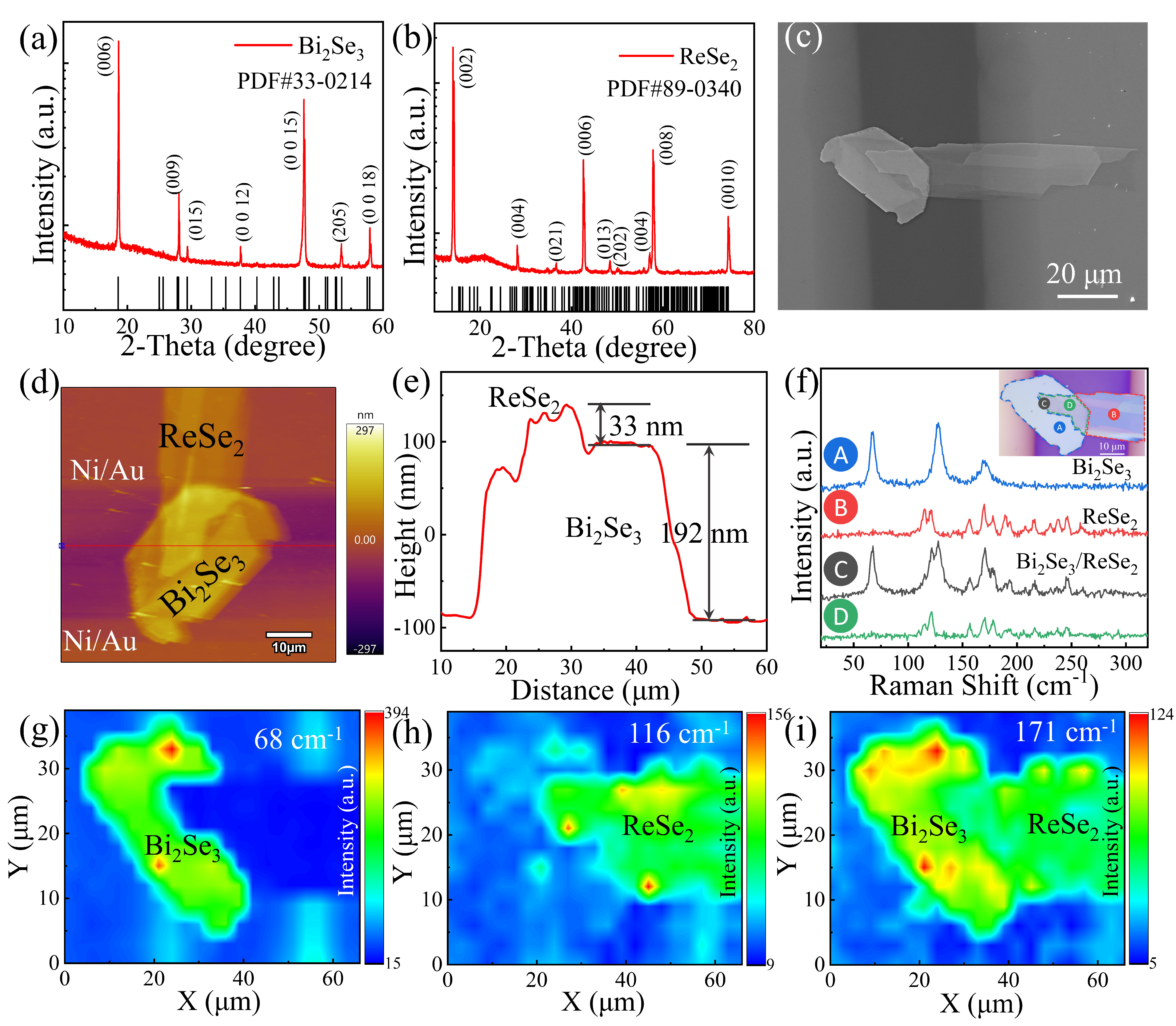
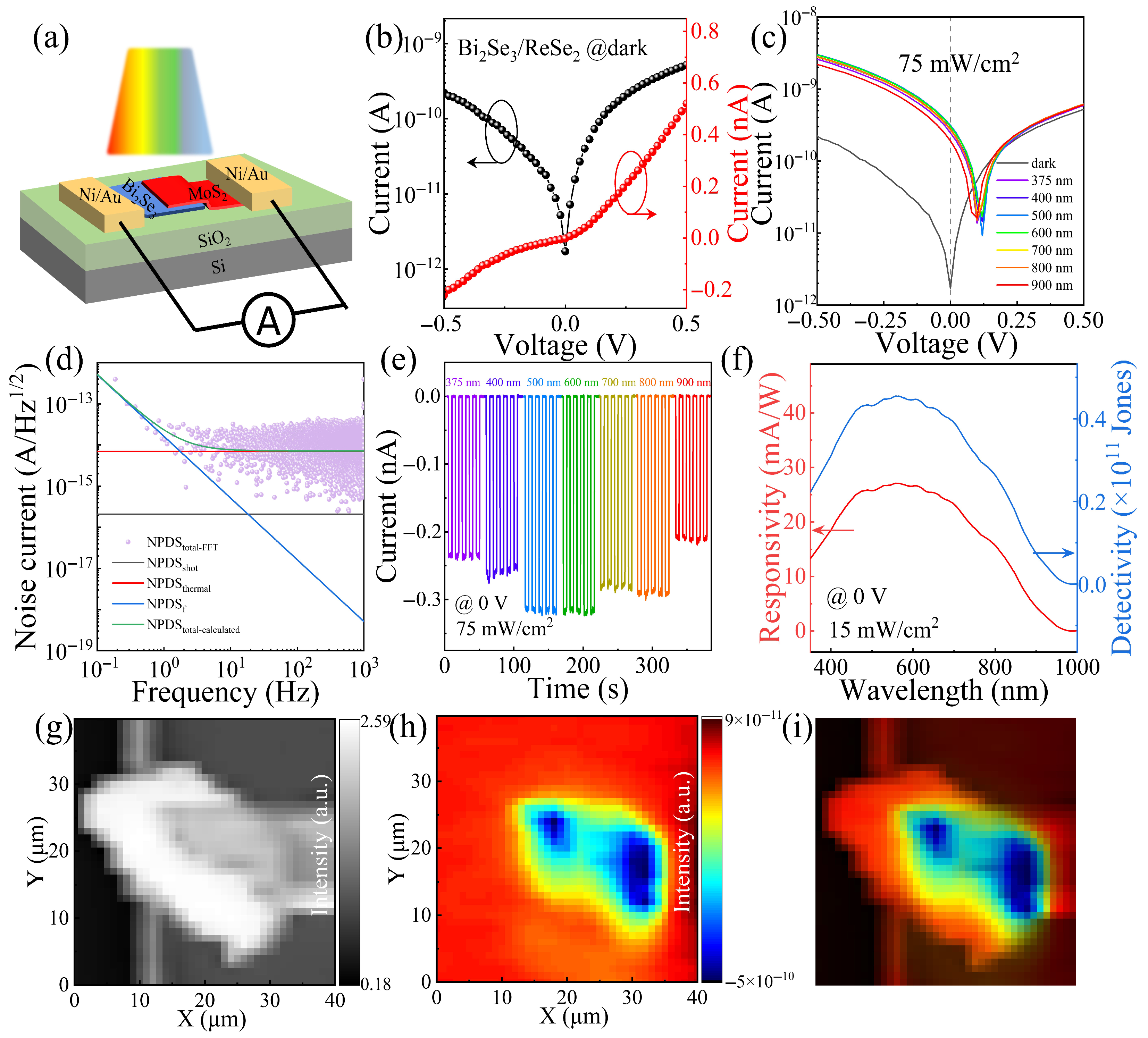
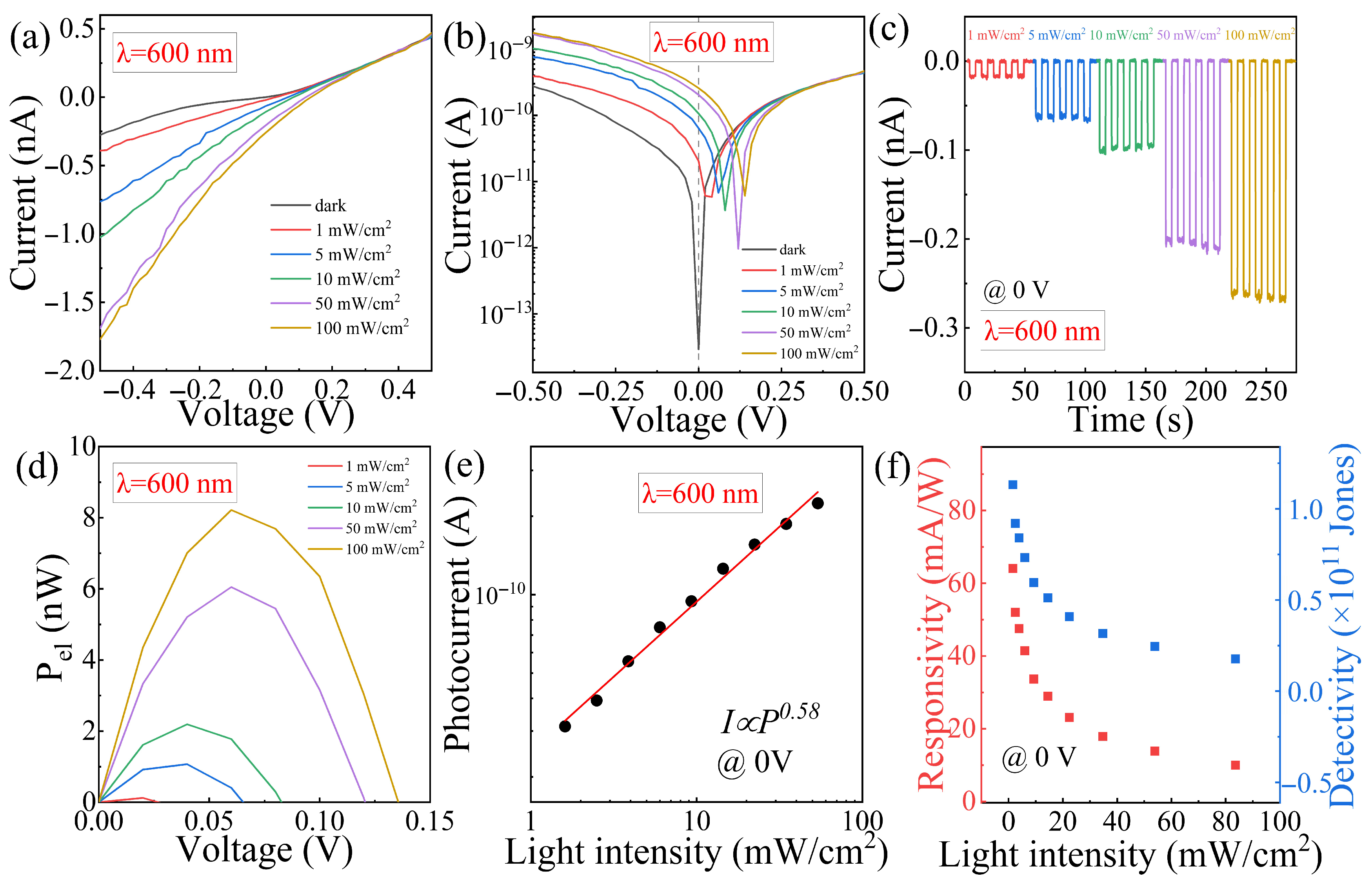
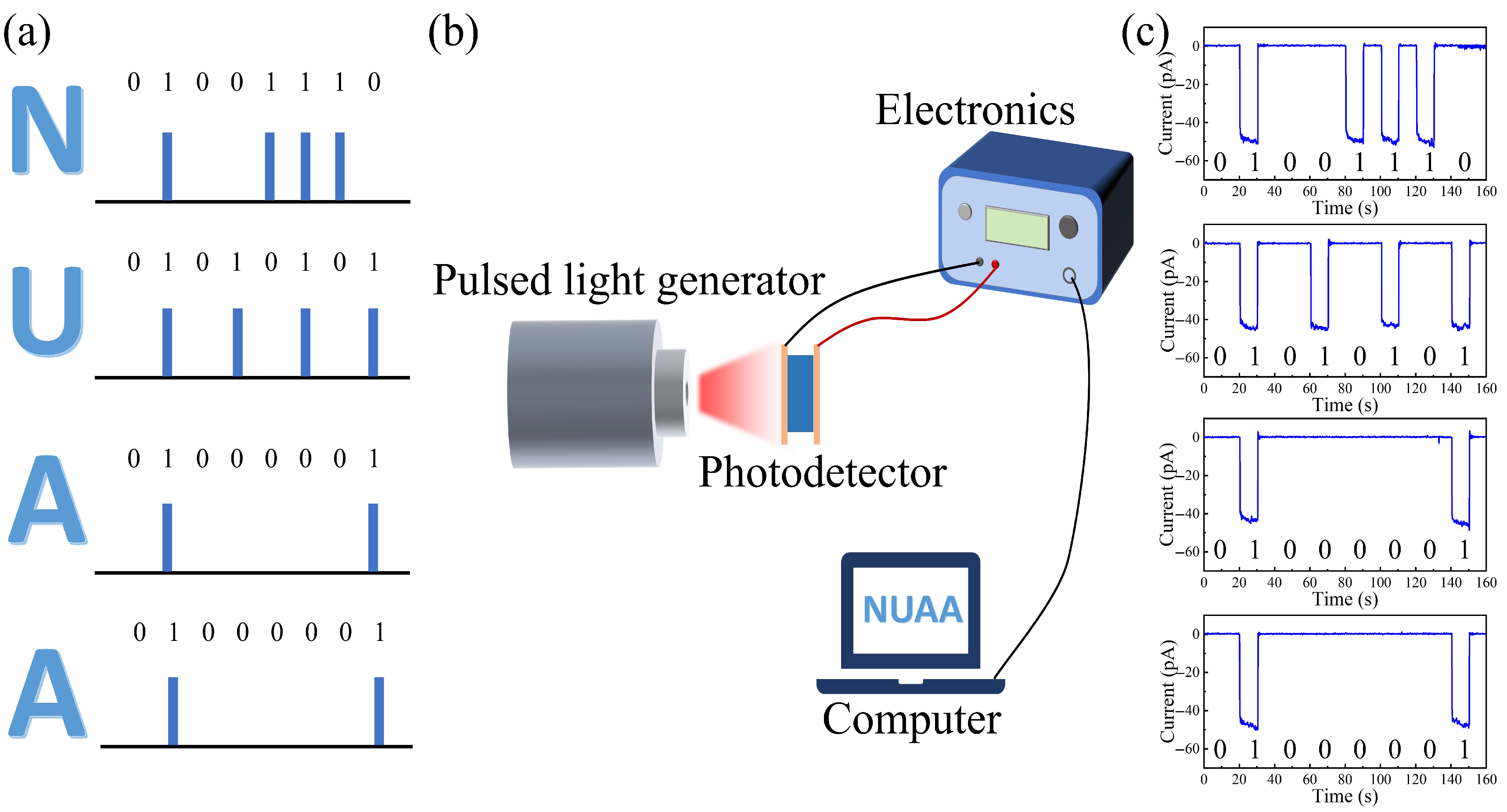
3. Results and Discussion

CVD method was used to grow the Bi 2 Se 3 TIs on the SiO 2 /Si substrate. As shown in Figure 1a, the prominent diffraction peaks of Bi 2 Se 3 flakes in XRD pattern are in good agreement with the standard PDF card (JCPDS No. 33-0214) [20]. At roughly 18 . 6 , the XRD peak represents the (006) crystal plane of Bi 2 Se 3 . The pronounced intensity of the (00k) diffraction peaks suggests preferential orientation of the Bi 2 Se 3 TIs along the (001) cleavage plane [21]. The presence of peaks other than the (00k) planes in the XRD pattern suggests that not all Bi 2 Se 3 flakes are perfectly aligned along the [001] direction. In our experiment, we used multiple Bi 2 Se 3 flakes for XRD measurement due to the limits of the instrument, and it is expected that some flakes may not be perfectly horizontal or be stacked on top of each other. Thus, the peaks other than the (00k) planes in the XRD pattern are present. Figure 1b presents the XRD pattern of the ReSe 2 single crystal, which is consistent with JCPDS No. 89-0340. It is evident that ReSe 2 is aligned along the (001) plane. The narrow XRD peaks indicate high crystalline quality, providing a solid foundation for the subsequent fabrication of Bi 2 Se 3 /ReSe 2 heterojunction.
The Bi 2 Se 3 /ReSe 2 heterojunction photodetector was fabricated via a PDMS-assisted transfer method. The detailed fabrication is available in Materials and Methods section. The SEM image depicting the device is displayed in Figure 1c. It is evident that the overlapping region of the Bi 2 Se 3 /ReSe 2 structure is extremely clean, without any residual impurities. The thicknesses of the Bi 2 Se 3 and ReSe 2 heterojunction were measured using AFM (Figure 1d). As shown in Figure 1e, it can be seen that Bi 2 Se 3 flake has a relatively large thickness (∼200 nm), while ReSe 2 flack is thinner (∼30 nm). The chemical composition of the heterojunction was characterized by EDS analysis (Figure S1, Supplementary Information). The Bi element originates from the Bi 2 Se 3 , while the Se element comes from both Bi 2 Se 3 and ReSe 2 . The Re element is detected throughout the entire mapped area due to the spectrum that the signals of Si from substrate and Re overlap.
As shown in the inset of Figure 1f, four regions were defined on the heterojunction: pure Bi 2 Se 3 at point A, pure ReSe 2 at point B, the Bi 2 Se 3 /ReSe 2 boundary at point C, and the Bi 2 Se 3 /ReSe 2 junction at point D. Raman spectra of various regions are presented in Figure 1f. For the individual Bi 2 Se 3 TIs (point A), three Raman peaks can be seen at 68, 128, and 171 cm 1 , corresponding to the A 1 g 1 , E g 2 and A 1 g 2 modes, in agreement with earlier studies [22,23]. For the individual ReSe 2 flake (point B), it can be observed that numerous Raman peaks exist within the testing range. The ReSe 2 unit cell comprises 12 atoms, which leads to the anticipation of 36 Raman vibrational modes. Based on the point group symmetry of the ReSe 2 , 18 of these modes are Raman-active [24]. The measured Raman spectrum of ReSe 2 is consistent with previous studies [25]. In the boundary region between the Bi 2 Se 3 and ReSe 2 (point C), characteristic Raman peaks of both materials are clearly discernible. This indicates a strong coupling effect between Bi 2 Se 3 and ReSe 2 . In the overlapped junction region (point D), Bi 2 Se 3 Raman signals are undetectable. This results from the relatively large thickness of the ReSe 2 flake (except at the edges), which exceeds the excitation light’s penetration depth. Figure 1g–i show the Raman mapping images at 68 cm 1 ( A 1 g 1 mode in Bi 2 Se 3 ), 116 cm 1 ( A g mode in ReSe 2 ) and 171 cm 1 ( A 1 g 2 mode in Bi 2 Se 3 and A g mode in ReSe 2 ). It can be intuitively observed that the Bi 2 Se 3 TIs and ReSe 2 form an effective coupling.
As shown in Figure 2a, a schematic diagram of the prepared Bi 2 Se 3 /ReSe 2 heterojunction device is presented. Figure 2b illustrates the I-V characteristic curves for the Bi 2 Se 3 /ReSe 2 device under dark conditions, presented in both linear and logarithmic scales. The I-V curves exhibit obvious rectifying behavior, with a rectification ratio of 2.35. As illustrated in Figure 2c, the log I-V characteristics were measured using different incident light wavelengths at a fixed light power density (75 mW/cm 2 ). Under different wavelength illumination conditions, Bi 2 Se 3 /ReSe 2 photodetector demonstrates excellent photoresponse characteristics, indicating that the device have wide-band response capabilities. In addition, the photodetector demonstrates a significant ratio of photocurrent to dark current ( I ph / I d ) at 0 V, demonstrating that the device is capable of self-powered operation. The noise characteristics of the Bi 2 Se 3 /ReSe 2 photodetector at zero bias, as depicted in Figure 2d, were examined. The total noise ( i n ) of the device is determined by shot noise ( i shot ), flicker noise ( i 1 / f ), and thermal noise ( i thermal ) collectively. The noise of the device is calculated by the following formula [26,27]:
i shot 2 = 2 q I d Δ f ,
i 1 / f 2 = C I d β / f α Δ f ,
i thermal 2 = 4 k T Δ f / R s ,
i n 2 = i shot 2 + i 1 / f 2 + i thermal 2 .
where I d , Δ f , f, and R s represent the dark current, electronic bandwidth, frequency, and shunt resistance, respectively. C, α , β are constants. The i n measured (obtained by performing a fast Fourier transform on the time-domain I d ) is closely matched to the total noise calculated. At 0 V bias, the device’s noise is dominated by flicker noise at frequencies below 1 Hz, while thermal noise prevails at higher frequencies [28]. The flicker noise of the photodetector may be related to the topological insulating properties of Bi 2 Se 3 . Previous research has demonstrated that the microscopic origins of 1/f noise observed on the surface of Bi 2 Se 3 stem from the interactions between Dirac electrons and the thermal motion of selenium (Se) and bismuth (Bi) atoms [29]. The amplitude of 1/f noise in TIs may also be related to thickness; when the thickness is appropriate, the noise amplitude is significantly low [30]. In contrast, carriers in conventional semiconductor heterojunctions may originate from both the bulk and interfaces, with bulk defect scattering exacerbating noise [27,31].
To evaluate the wide-band photodetection performance of the device, we conducted detailed tests. Figure 2e illustrates the I-T curves for various illumination conditions while maintaining a constant optical power. The curve maintains consistent photocurrent as the on–off cycle increases, demonstrating excellent stability and repeatability. Responsivity (R) is critical, as it denotes the device’s capability to transform incident optical signals into electrical outputs. Additionally, specific detectivity ( D ) and noise equivalent power (NEP) stand as key parameters for evaluating photodetector performance. R, NEP, and D are computed via the subsequent equations [32]:
R = I ph I d P S
NEP = I n 2 R
D = S Δ f NEP
where I ph , I d , P, S, I n 2 , and Δ f correspond to photocurrent, dark current, light power density, effective area (≈ 3 × 10 7 cm 2 ), noise current power, and bandwidth. Figure 2f illustrates the wavelength-dependent R and D under constant power density of 15 mW/cm 2 . The Bi 2 Se 3 /ReSe 2 photodetector’s R and D rise gradually from 350 nm, peak near 600 nm, then decline at longer wavelengths, with a broad 350–900 nm spectral response. At 600 nm, the R and D reach 26.6 mA/W and 4.5 × 10 10 Jones, respectively. To study the response region of the photodetector, photocurrent mapping was measured via micro-area laser scanning. Figure 2g presents a reference image of light intensity, which is derived from the collected reflected light when the sample is illuminated by a laser. As illustrated in Figure 2h, a photocurrent mapping image measured under 638 nm laser irradiation is presented at 0 V voltage. Figure 2i is the fused image of Figure 2g,h. The prominent photoresponse is predominantly localized in the heterojunction region of Bi 2 Se 3 and ReSe 2 .
Figure 3a presents the photocurrent and dark current curves of the Bi 2 Se 3 /ReSe 2 photodetector at 0 V, obtained by adjusting the irradiance of the incident 600 nm LED within the range of 1 to 100 mW/cm 2 . The corresponding logarithmic curves are displayed in Figure 3b. When the light’s power density goes up, the photocurrent increases steadily. This is because more electron–hole pairs are generated in the illuminated area of the heterojunction. A significant difference between the photocurrent and the dark current when subjected to zero and reverse biases demonstrates the exceptional on–off ratio and high sensitivity of the Bi 2 Se 3 /ReSe 2 photodetector to 600 nm light. The I-T curves of the Bi 2 Se 3 /ReSe 2 photodetector were recorded under pulsed 600 nm illumination at power densities from 1 to 100 mW/cm 2 , as shown in Figure 3c. The current rises rapidly and remains stable upon light illumination, and once the light is switched off, it rapidly returns to its original state. “ON”/“OFF” state currents stay stable per cycle, further confirming the device’s excellent reversibility and stability. With light intensity upped to mW/cm 2 (starting at 1 mW/cm 2 ), the photocurrent creeps up to 265 pA (beginning at 18 pA) under zero bias. The device’s notable self-powered performance stems from the built-in electric field at the Bi 2 Se 3 /ReSe 2 interface, which enables effective separation of photo-induced carriers. Additionally, the electricity generation ability of a photovoltaic detector may be described via the output electric power ( P el ), formulated as:
P el = I ph V Bias
Figure 3d illustrates the P el of the Bi 2 Se 3 /ReSe 2 device varying with the bias voltage at various light intensities. The continuous upward trend observed in the I-V characteristic curve indicates that the peak P el rises in parallel with the enhancement of light power density. The highest P el reaches 8.2 nW when a bias voltage of 60 mV is applied, with the incident light intensity set at 100 mW/cm 2 . Figure 3e shows the light irradiance-dependent photocurrent. The relationship between I and P can be well fitted as:
I = A P θ
where A acts as a constant, and θ stands for the power law factor. Through logarithmic fitting of the photocurrent-intensity data, θ is found to be 0.58, indicating a sublinear dependence. Kalimuddin et al. pointed out that the sublinear relationship between photocurrent and incident light power is related to topological surface states [33]. Figure 3f shows the R and D of the Bi 2 Se 3 /ReSe 2 photodetector at different power densities. The photodetector achieves maximum R of 64 mA/W and D of 1.1 × 10 11 Jones when illuminated at 600 nm with a light power density of 1 mW/cm 2 . In addition, the R and D of the photodetector exhibit a downward trend with increasing light density, primarily due to intensified carrier recombination caused by high-intensity light irradiation.
As shown in Figure 4a, the photodetector response to 638 nm pulsed light at modulation frequencies of 0.05, 0.3, 0.5, 1, and 4 kHz is demonstrated. It is evident that the photodetector demonstrates rapid and stable frequency response, confirming its stable performance across frequencies. As the pulsed light frequency rises, the waveform transitions from a square to a distorted triangular shape, attributed to limited carrier response speed at high frequencies. In order to obtain the photodetector’s effective response speed, we further examined and graphed the normalized intensity of photocurrent amplitude as it relates to modulation frequency, as shown in Figure 4b. With an increase in modulation frequency, the photocurrent amplitude decreases. The 3 dB bandwidth, which is identified as the frequency where the amplitude of the photocurrent decreases to 70.7% of its low-frequency level, is used to describe how quickly the device responds [34]. It has been ascertained that the 3 dB bandwidth of the Bi 2 Se 3 /ReSe 2 photodetector is 1.4 kHz. Thus, it is reasonable to use the 500 Hz response curve for calculating the photodetector’s response speed, given its stable waveform characteristics. Response time refers to the time duration for photocurrent amplitude to rise from 10% to 90% (rise time) or fall from 90% to 10% (fall time). As depicted in Figure 4c, the response speed is calculated at a frequency of 500 Hz. At 0 V bias, the Bi 2 Se 3 /ReSe 2 photodetector exhibits a rapid response speed of 345 μ s rise/336 μ s fall time.
We conducted multi-cycle tests to evaluate the short-term stability of the photodetectors. The results showed that the photodetectors maintained consistent performance over multiple cycles, indicating good short-term stability (see Figure 4d). However, in long-term tests conducted over several days, we observed that while the photodetectors remained stable in the short term, their sensitivity began to decline over extended periods (Figure S2). This aging effect is primarily due to environmental factors such as humidity, temperature, and oxygen, which can degrade the material properties over time. For practical application, encapsulation can help protect the 2D materials from environmental degradation, thereby improving their long-term stability. Different Bi 2 Se 3 flakes and ReSe 2 flakes with similar thickness were selected to construct Bi 2 Se 3 /ReSe 2 heterojunction photodetectors. To evaluate the reproducibility of our photodetectors, we conducted multiple tests on 10 different devices. As shown in Figure S3, there was some variation in the experimental data, which can be attributed to the surface roughness and crystallinity of the as-prepared samples. Although there was some variation in the experimental data, the overall performance remained within a consistent range. This indicates that our fabrication process and material selection are reliable and reproducible. A comparative analysis of the performance characteristics between heterojunction detectors incorporating Bi 2 Se 3 and other non-Bi 2 Se 3 heterojunction detectors (see Table 1) reveals that devices utilizing TIs demonstrate significantly fast response speeds. This notable enhancement in temporal performance can be directly attributed to the unique properties of the topological surface states inherent in these materials. The surface states serves as a highly efficient, high-mobility charge transport channel within the detector structure, facilitating rapid carrier collection and thereby substantially improving the overall response dynamics.
The electrical transport characteristics of Bi 2 Se 3 flakes were assessed using field-effect transistors (FETs) based on Bi 2 Se 3 flakes. Figure 5a displays the optical picture of the Bi 2 Se 3 flake-based FET. Figure S4 presents the schematic illustration of the FET structure. Figure 5b displays the relationship between the source–drain current ( I d s ) and the source–drain voltage ( V d s ) across various back-gate voltages ( V g ). By varying the V g , the I d s was determined, as shown in Figure 5c. The results demonstrate typical n-channel FET output characteristics, namely that Bi 2 Se 3 conductance increases (decreases) when positive (negative) V g increases. Notably, the increase or decrease is less evident in Bi 2 Se 3 because of its high conductance and the metallic characteristics of its surfaces, compared to nanowire-based FETs. The carrier mobility ( μ ) of Bi 2 Se 3 can be expressed as [35]:
μ = g m L W c p V d s
c p = ε 0 ε r d
where g m is the transconductance of the Bi 2 Se 3 FET, L represents the channel length (7.5 μ m), W denotes the channel width (14.3 μ m), c p is the capacitance per unit area, ε 0 refers to the vacuum permittivity, ε r signifies the relative dielectric constant of the SiO 2 layer (3.9), and d represents the thickness of the SiO 2 layer (∼300 nm). The calculated value of μ is 158.8 cm 2 /(V·s). Topological protection is the primary enabler of high mobility; the measured value is ultimately governed by the interplay of residual scattering mechanisms (e.g., phonon scattering, magnetic impurities, defects) and potential coupling to bulk states [11,13].
To comprehend the carrier transport behavior of the heterostructure, the band alignment of the Bi 2 Se 3 /ReSe 2 heterostructure is analyzed. The valence band maximum (E v ) and conduction band minimum (E c ) of ReSe 2 (Bi 2 Se 3 ) are located at −5.06 eV (−5.21 eV) and −3.92 eV (−4.91 eV), respectively [22,36]. The energy bandgaps of ReSe 2 and Bi 2 Se 3 are 1.14 and 0.3 eV, respectively. The band diagrams for Bi 2 Se 3 and ReSe 2 without contacts are illustrated in Figure 5d. The Fermi level of ReSe 2 is higher than that of Bi 2 Se 3 because the larger surface potential results in a lower work function, which in turn leads to a higher Fermi level [37]. At thermal equilibrium with a voltage of 0 V, Figure 5e illustrates the energy diagram of the Bi 2 Se 3 /ReSe 2 heterostructure. Once they are in contact with each other, a built-in potential would form on the side of ReSe 2 . The inherent potential difference between ReSe 2 and Bi 2 Se 3 facilitates the effective separation of electron and hole pairs generated by light. In the zero-bias condition, the photocurrent in the external circuit would be created by injecting the holes of ReSe 2 into the Bi 2 Se 3 side and transferring the electrons of ReSe 2 to the Ni/Au electrode. The favorable mobility of Bi 2 Se 3 flake significantly enhances charge transfer at the interface and improves the efficiency of separation for photo-generated carriers within the built-in electric field. In addition, this separation mechanism is associated with the topological protection of surface states (e.g., backscattering resistance), significantly reducing carrier recombination [12]. The surface states of Bi 2 Se 3 flake acts as a transport channel, enabling the extraction and transfer of photo-generated carriers that are separated by the inherent electric field. Due to its favorable mobility, it provides an energetically efficient pathway for the transportation and collection of carriers within the photodetector, thereby enhancing the photoresponse (Figure 5f).
Table 1. Comparison between the reported 2D photodetectors and this work.
PhotodetectorSelf-Powered
(0 V Bias)
Wavelength [nm]Responsivity [mA/W]Rise Time/Fall TimeRef.
Bi 2 Se 3 /Sino8086.96 × 10 3 (5 V)19.7 μ s/35.2 μ s[38]
Bi 2 Se 3 /SnTeyes1550145.74 (0 V)6.9 μ s/19.2 μ s[39]
Bi 2 Se 3 /Siyes8082.43 × 10 4 (−1 V)2.5 μ s/5.5 μ s[40]
InSe/ReSe 2 no6381.61 × 10 4 (2 V)360 μ s/390 μ s[41]
Bi 2 S 3 /MoS 2 yes4200.218 (0 V)4 ms/15 ms[42]
Bi 2 Se 3 /ReSe 2 yes60064 (0 V)345 μ s/336 μ sThis work
Based on the fast response speed of Bi 2 Se 3 /ReSe 2 photodetectors, the potential of the device as an optical communication photoreceiver was investigated. The effective data rate were determined by the modulation speed of the LED source and the 3 dB bandwidth of the device. Given the 3 dB bandwidth of 1.4 kHz, the maximum theoretical data rate can be estimated as 2.8 kbps using the Nyquist formula for the maximum data rate in a noiseless channel. However, the primary limitation in our experiment is the modulation speed of the LED source. The LED’s maximum modulation speed of 50 Hz directly constrains the data rate to 50 bps. As shown in Figure 6a, ‘NUAA’ is ASCII-encoded for optical transmission, with each character converted to an 8-bit binary string [43]. Pulsed light signals are modulated based on these binary strings, with ‘1’ corresponding to light-on and ‘0’ to light-off. Figure 6b illustrates the schematic diagram of photodetector optical signal detection. Using precisely controlled 600-nanometer LEDs as signal transmitters. The Bi 2 Se 3 /ReSe 2 photodetectors serve as signal receivers, generating equivalent photocurrent under self-powered conditions. The photocurrent is read by electronic devices and decoded by a computer. The optical signal response measured by the Bi 2 Se 3 /ReSe 2 photodetector during the experiment is plotted in Figure 6c. It is evident that the photodetector accurately identified the output optical signals, thus ensuring the correct transmission of alphabetic information. Experimental results suggest that the fabricated photodetector possesses promising potential for optical communication applications.

4. Conclusions

We propose a novel combination of TIs (Bi 2 Se 3 ) and ReSe 2 for high sensitivity self-powered photodetectors, achieving broadband response spectra up to 1 μ m, a high responsivity of 64 mA/W at 600 nm (1 mW/cm 2 ), 3 dB bandwidth of 1.4 kHz, and a fast response speed of 345 μ s rise/336 μ s fall time at zero bias. The appropriate energy band structure of Bi 2 Se 3 /ReSe 2 and the high carrier mobility in surface states of Bi 2 Se 3 are responsible for the high performance. Interestingly, self-powered topological insulator photodetectors enable high-quality broadband signal transmission, and the topological insulator used in photodetectors can stimulate the production of new optoelectronic features, but it can also be used for highly integrated photonic circuits in the future.

Supplementary Materials

The following supporting information can be downloaded at: https://www.mdpi.com/article/10.3390/photonics12070709/s1, Figure S1. EDS analysis of the Bi2Se3/ReSe2 photodetector. The inset shows the EDS mapping results of Bi, Se and Re elements. Figure S2. Changes in photocurrent and dark current of the self-powered Bi2Se3/ReSe2 photodetector placed in the laboratory at different times. Figure S3. (a) Responsivity and (b) rise/fall time of the ten Bi2Se3/ReSe2 heterojunction photodetectors. Figure S4. Schematic illustration of the Bi2Se3 flake-based FET.

Author Contributions

Y.W.: conceptualization, sample preparation, device fabrication, formal analysis, and writing—original draft preparation. P.W.: conceptualization, methodology, validation, and funding acquisition. L.L.: conceptualization, and formal analysis. T.H.: device fabrication, characterization, conceptualization, methodology. W.M.: validation, resources, and methodology. T.X.: conceptualization, methodology. B.Y.: device fabrication, characterization. S.S.: resources, and methodology. C.K.: funding acquisition and supervision. M.J.: funding acquisition, supervision, and writing—review. All authors have read and agreed to the published version of the manuscript.

Funding

This study was supported by the National Natural Science Foundation of China (Grant Nos. 11974182 and 11874220) and the Fundamental Research Funds for the Central Universities (NO. NC2022008).

Data Availability Statement

The data presented in this study are available from the corresponding author upon reasonable request.

Conflicts of Interest

The authors declare no conflicts of interest.

References

  1. Xie, Y.; Zhang, B.; Wang, S.; Wang, D.; Wang, A.; Wang, Z.; Yu, H.; Zhang, H.; Chen, Y.; Zhao, M.; et al. Ultrabroadband MoS2 photodetector with spectral response from 445 to 2717 nm. Adv. Mater. 2017, 29, 1605972. [Google Scholar] [CrossRef] [PubMed]
  2. Shanmugam, V.; Mensah, R.A.; Babu, K.; Gawusu, S.; Chanda, A.; Tu, Y.; Neisiany, R.E.; Försth, M.; Sas, G.; Das, O. A review of the synthesis, properties, and applications of 2D materials. Part. Part. Syst. Charact. 2022, 39, 2200031. [Google Scholar] [CrossRef]
  3. Long, M.; Wang, P.; Fang, H.; Hu, W. Progress, challenges, and opportunities for 2D material based photodetectors. Adv. Funct. Mater. 2019, 29, 1803807. [Google Scholar] [CrossRef]
  4. Chen, X.; Rogers, J.A.; Lacour, S.P.; Hu, W.; Kim, D.H. Materials chemistry in flexible electronics. Chem. Soc. Rev. 2019, 48, 1431–1433. [Google Scholar] [CrossRef] [PubMed]
  5. Pang, Y.; Yang, Z.; Yang, Y.; Ren, T.L. Wearable electronics based on 2D materials for human physiological information detection. Small 2020, 16, 1901124. [Google Scholar] [CrossRef]
  6. Island, J.O.; Steele, G.A.; van der Zant, H.S.; Castellanos-Gomez, A. Environmental instability of few-layer black phosphorus. 2D Mater. 2015, 2, 011002. [Google Scholar] [CrossRef]
  7. Shen, X.; Lin, X.; Peng, Y.; Zhang, Y.; Long, F.; Han, Q.; Wang, Y.; Han, L. Two-dimensional materials for highly efficient and stable perovskite solar cells. Nano-Micro Lett. 2024, 16, 201. [Google Scholar] [CrossRef]
  8. Dziobek-Garrett, R.; Imperiale, C.J.; Wilson, M.W.; Kempa, T.J. Photon upconversion in a vapor deposited 2D inorganic–organic semiconductor heterostructure. Nano Lett. 2023, 23, 4837–4843. [Google Scholar] [CrossRef]
  9. Qi, X.L.; Zhang, S.C. Topological insulators and superconductors. Rev. Mod. Phys. 2011, 83, 1057–1110. [Google Scholar] [CrossRef]
  10. Zhang, H.; Liu, C.X.; Qi, X.L.; Dai, X.; Fang, Z.; Zhang, S.C. Topological insulators in Bi2Se3, Bi2Te3 and Sb2Te3 with a single Dirac cone on the surface. Nat. Phys. 2009, 5, 438–442. [Google Scholar] [CrossRef]
  11. Steinberg, H.; Gardner, D.R.; Lee, Y.S.; Jarillo-Herrero, P. Surface state transport and ambipolar electric field effect in Bi2Se3 nanodevices. Nano Lett. 2010, 10, 5032–5036. [Google Scholar] [CrossRef] [PubMed]
  12. Sun, J.; Singh, D.J. Using gapped topological surface states of Bi2Se3 films in a field effect transistor. J. Appl. Phys. 2017, 121, 064301. [Google Scholar] [CrossRef]
  13. Yan, Y.; Wang, L.X.; Yu, D.P.; Liao, Z.M. Large magnetoresistance in high mobility topological insulator Bi2Se3. Appl. Phys. Lett. 2013, 103, 033106. [Google Scholar] [CrossRef]
  14. Das, S.K.; Sahoo, U.P.; Das, B.; Ghorai, G.; Samal, P.; Sahoo, P.K. Defect induced unconventional ferromagnetism in Au intercalated Bi2Se3 nanocrystals for spintronic applications. Adv. Quantum Technol. 2023, 6, 2300169. [Google Scholar] [CrossRef]
  15. Li, J.; Chang, K. Electric field driven quantum phase transition between band insulator and topological insulator. Appl. Phys. Lett. 2009, 95, 222110. [Google Scholar] [CrossRef]
  16. Besbas, J.; Banerjee, K.; Son, J.; Wang, Y.; Wu, Y.; Brahlek, M.; Koirala, N.; Moon, J.; Oh, S.; Yang, H. Helicity-dependent photovoltaic effect in Bi2Se3 under normal incident light. Adv. Opt. Mater. 2016, 4, 1642–1650. [Google Scholar] [CrossRef]
  17. Li, Y.; Wang, S.; Hong, J.; Zhang, N.; Wei, X.; Zhu, T.; Zhang, Y.; Xu, Z.; Liu, K.; Jiang, M.; et al. Polarization-sensitive photodetector based on high crystallinity Quasi-1D BiSeI nanowires synthesized via chemical vapor deposition. Small 2023, 19, 2302623. [Google Scholar] [CrossRef]
  18. Linghu, C.; Zhang, S.; Wang, C.; Song, J. Transfer printing techniques for flexible and stretchable inorganic electronics. NPJ Flex. Electron. 2018, 2, 26. [Google Scholar] [CrossRef]
  19. Du, K.; Wathuthanthri, I.; Liu, Y.; Xu, W.; Choi, C.H. Wafer-scale pattern transfer of metal nanostructures on polydimethylsiloxane (PDMS) substrates via holographic nanopatterns. ACS Appl. Mater. Interfaces 2012, 4, 5505–5514. [Google Scholar] [CrossRef]
  20. Ermolaev, G.A.; Vyslanko, I.S.; Tselin, A.P.; El-Sayed, M.A.; Tatmyshevskiy, M.K.; Slavich, A.S.; Yakubovsky, D.I.; Mironov, M.S.; Mazitov, A.B.; Eghbali, A.; et al. Broadband optical properties of Bi2Se3. Nanomaterials 2023, 13, 1460. [Google Scholar] [CrossRef]
  21. Atuchin, V.; Golyashov, V.; Kokh, K.; Korolkov, I.; Kozhukhov, A.; Kruchinin, V.; Makarenko, S.; Pokrovsky, L.; Prosvirin, I.; Romanyuk, K.; et al. Formation of inert Bi2Se3 (0001) cleaved surface. Cryst. Growth Des. 2011, 11, 5507–5514. [Google Scholar] [CrossRef]
  22. Wang, F.; Luo, P.; Zhang, Y.; Huang, Y.; Zhang, Q.; Li, Y.; Zhai, T. Band structure engineered tunneling heterostructures for high-performance visible and near-infrared photodetection. Sci. China Mater. 2020, 63, 1537–1547. [Google Scholar] [CrossRef]
  23. Ma, J.; Chen, S.; Zhao, L.; Chen, J.; Lan, Z.; Yang, M.; Sun, Y.; Zheng, Z.; Gao, W.; Li, J. 2D double heterostructure infrared photodetector with Type-III band alignment by incorporating Bi2Se3 Layer. Adv. Opt. Mater. 2024, 12, 2302563. [Google Scholar] [CrossRef]
  24. Wolverson, D.; Crampin, S.; Kazemi, A.S.; Ilie, A.; Bending, S.J. Raman spectra of monolayer, few-layer, and bulk ReSe2: An anisotropic layered semiconductor. ACS Nano 2014, 8, 11154–11164. [Google Scholar] [CrossRef]
  25. Pradhan, N.R.; Garcia, C.; Isenberg, B.; Rhodes, D.; Feng, S.; Memaran, S.; Xin, Y.; McCreary, A.; Walker, A.R.H.; Raeliarijaona, A.; et al. Phase modulators based on high mobility ambipolar ReSe2 field-effect transistors. Sci. Rep. 2018, 8, 12745. [Google Scholar] [CrossRef]
  26. Jahromi, H.D.; Lotfiani, A. A fast and sensitive Schottky photodiode with surface plasmon enhanced photocurrent and extremely low dark current for high-frequency applications in near-infrared. IEEE Sens. J. 2022, 22, 20430–20437. [Google Scholar] [CrossRef]
  27. Jahromi, H.D.; Mahmoodi, A.; Sheikhi, M.H.; Zarifkar, A. Spectral response, dark current, and noise analyses in resonant tunneling quantum dot infrared photodetectors. Appl. Opt. 2016, 55, 8494–8499. [Google Scholar] [CrossRef]
  28. Chen, S.; Fu, Y.; Ishaq, M.; Li, C.; Ren, D.; Su, Z.; Qiao, X.; Fan, P.; Liang, G.; Tang, J. Carrier recombination suppression and transport enhancement enable high-performance self-powered broadband Sb2Se3 photodetectors. InfoMat 2023, 5, e12400. [Google Scholar] [CrossRef]
  29. Mihaila, M.; Varasteanu, P. Surface phonons in the 1/f noise of Bi2Se3. Appl. Phys. Lett. 2025, 126, 032202. [Google Scholar] [CrossRef]
  30. Bhattacharyya, S.; Banerjee, M.; Nhalil, H.; Islam, S.; Dasgupta, C.; Elizabeth, S.; Ghosh, A. Bulk-induced 1/f noise at the surface of three-dimensional topological insulators. ACS Nano 2015, 9, 12529–12536. [Google Scholar] [CrossRef]
  31. Mahmoodi, A.; Jahromi, H.D.; Sheikhi, M.H. Dark current modeling and noise analysis in quantum dot infrared photodetectors. IEEE Sens. J. 2015, 15, 5504–5509. [Google Scholar] [CrossRef]
  32. Zheng, D.; Fang, H.; Wang, P.; Luo, W.; Gong, F.; Ho, J.C.; Chen, X.; Lu, W.; Liao, L.; Wang, J.; et al. High-performance ferroelectric polymer side-gated CdS nanowire ultraviolet photodetectors. Adv. Funct. Mater. 2016, 26, 7690–7696. [Google Scholar] [CrossRef]
  33. Kalimuddin, S.; Das, B.; Chatterjee, S.; Bera, A.; Bera, S.; Chattopadhyay, K.; Mondal, M. Low-frequency 1/f noise and barrier height inhomogeneity in topological insulator-based photodetectors. ACS Appl. Mater. Interfaces 2025, 17, 35781–35789. [Google Scholar] [CrossRef] [PubMed]
  34. Buscema, M.; Groenendijk, D.J.; Blanter, S.I.; Steele, G.A.; Van Der Zant, H.S.; Castellanos-Gomez, A. Fast and broadband photoresponse of few-layer black phosphorus field-effect transistors. Nano Lett. 2014, 14, 3347–3352. [Google Scholar] [CrossRef]
  35. Shiju, K.; Praveen, T.; Aneesh, J.; Manuvel, J. Organic field effect transistor with conductivity enhanced PEDOT: PSS composite electrodes. AIP Conf. Proc. 2013, 1536, 1139–1140. [Google Scholar]
  36. Li, W.; Yang, R.; Han, X.; Cheng, L.; Yin, T.; Gao, K.; Gan, X.; Wang, Y.; Wang, S. Bias tunable SnS2/ReSe2 tunneling photodetector with high responsivity and fast response speed. Small 2025, 21, 2408379. [Google Scholar] [CrossRef]
  37. Yu, M.; Fang, C.; Han, J.; Liu, W.; Gao, S.; Huang, K. Construction of Bi2O2Se/Bi2Se3 van der Waals heterostructures for self-powered and broadband photodetectors. ACS Appl. Mater. Interfaces 2022, 14, 13507–13515. [Google Scholar] [CrossRef]
  38. Nandi, S.; Ghosh, K.; Meyyappan, M.; Giri, P. 2D MXene electrode-enabled high-performance broadband photodetector based on a CVD-grown 2D Bi2Se3 ultrathin film on Silicon. ACS Appl. Electron. Mater. 2023, 5, 6985–6995. [Google Scholar] [CrossRef]
  39. Zhang, H.; Song, Z.; Li, D.; Xu, Y.; Li, J.; Bai, C.; Man, B. Near-infrared photodetection based on topological insulator PN heterojunction of SnTe/Bi2Se3. Appl. Surf. Sci. 2020, 509, 145290. [Google Scholar] [CrossRef]
  40. Zhang, H.; Zhang, X.; Liu, C.; Lee, S.T.; Jie, J. High-responsivity, high-detectivity, ultrafast topological insulator Bi2Se3/silicon heterostructure broadband photodetectors. ACS Nano 2016, 10, 5113–5122. [Google Scholar] [CrossRef]
  41. Du, C.; Gao, H.; Du, W.; Li, J.; Leng, J.; Li, K.; Wang, W. High responsivity and broadband polarized photodetectors based on InSe/ReSe2 van der Waals heterostructures. J. Alloys Compd. 2022, 919, 165586. [Google Scholar] [CrossRef]
  42. Hui, J. Two-dimensional Bi2S3/MoS2 van der Waals heterostructure for self-powered photodetectors. Appl. Phys. Express 2023, 16, 015507. [Google Scholar] [CrossRef]
  43. Wu, C.; Zhao, T.; He, H.; Hu, H.; Liu, Z.; Wang, S.; Zhang, F.; Wang, Q.; Liu, A.; Wu, F.; et al. Enhanced performance of gallium-based wide bandgap oxide semiconductor heterojunction photodetector for solar-blind optical communication via oxygen vacancy electrical activity modulation. Adv. Opt. Mater. 2024, 12, 2302294. [Google Scholar] [CrossRef]
Figure 1. Characterization of the Bi 2 Se 3 /ReSe 2 photodetector. (a) XRD pattern of Bi 2 Se 3 . (b) XRD pattern of ReSe 2 . (c) SEM image of the photodetector. (d) AFM image of the photodetector. (e) Thickness of the Bi 2 Se 3 and ReSe 2 . (f) Raman spectra of four different regions: A, B, C, and D. (gi) Raman mapping of the 68, 116, and 171 cm 1 peaks, respectively.
Photonics 12 00709 g001
Figure 2. Photoresponse of the Bi 2 Se 3 /ReSe 2 photodetector. (a) Device schematic under illumination. (b) I-V characteristics in darkness. (c) Logarithmic I-V curves under light of different wavelengths. (d) Noise power density spectrum of 0 V time-domain dark current via Fourier transform. (e) I-T curves under irradiation of different wavelengths at 0 V (P = 75 mW/cm 2 ). (f) Wavelength-dependent responsivity and detectivity. (g) Spatial reference light intensity of the device. (h) Photocurrent mapping image measured at 0 V under 638 nm laser illumination. (i) The fused image of (g,h).
Photonics 12 00709 g002
Figure 3. Optoelectronic characteristics of the photodetector. (a) I-V characteristics in dark and under 600 nm light with varying power (linear). (b) I-V characteristics in dark and under 600 nm light with varying power (logarithmic). (c) I-T curves under 600 nm light with varying power at 0 V bias. (d) P el of the photodetector in relation to the bias voltage when illuminated at 600 nm with varying power densities. (e) Photocurrent measurements under 600 nm light at various power densities. (f) Power-dependent responsivity and detectivity under the irradiation of 600 nm light.
Photonics 12 00709 g003
Figure 4. Response speed of the Bi 2 Se 3 /ReSe 2 photodetector. (a) Photoresponse properties of the photodetector at frequencies of 0.05, 0.3, 0.5, 1, and 4 kHz. (b) Relationship between normalized photocurrent intensity and modulation frequency. (c) Photodetector’s response speed was measured at a frequency of 500 Hz. (d) The I-T curve under 300 cycles of optical switching, with an illumination of 2 mW/cm 2 at 600 nm.
Photonics 12 00709 g004
Figure 5. Bi 2 Se 3 -based FET and energy band structure. (a) Optical image of Bi 2 Se 3 -based FET. (b) I d s - V d s plots of the FET under varying V g . The inset displays a magnified view of the plots. (c) The I d s - V g curve corresponding to V d s = 0.1 V. Energy band diagrams of the Bi 2 Se 3 /ReSe 2 heterostructure before (d,e) after contact under illumination. (f) Diagram illustrating the movement of photogenerated carriers across the surface states of Bi 2 Se 3 .
Photonics 12 00709 g005
Figure 6. Optical communication of the Bi 2 Se 3 /ReSe 2 photodetector. (a) The ASCII code of “NUAA” is generated by modulating the output light source of a 600 nm LED. (b) Schematic diagram of the photodetector detection. (c) The photoresponse of the Bi 2 Se 3 /ReSe 2 photodetector to modulated pulsed optical signals.
Photonics 12 00709 g006
Disclaimer/Publisher’s Note: The statements, opinions and data contained in all publications are solely those of the individual author(s) and contributor(s) and not of MDPI and/or the editor(s). MDPI and/or the editor(s) disclaim responsibility for any injury to people or property resulting from any ideas, methods, instructions or products referred to in the content.

